Note: Descriptions are shown in the official language in which they were submitted.
0 4 7 4 ~ ~ 72689-35
SEMICONDUCTOR L1EVICE AND
METHOD FO:R MANUFACTURING THE SAME
13ACKGROUN1~ OF THE INVENTION
The present invention relates to a semiconductor device
;end method for manufacturing the same. More specifically the
invention relates to a semiconductor device in which the moisture
impermeability of an airtight sealed semiconductor package is
increased, and a method of manufacturing the same.
In semiconductor chips such as IC, LSI or VLSI, the
1~~ highly integrated circuits surface tend to be affected by the
.changes i:n ambient temperature or humidity, or fine dust.
:Further, because a semiconductor chip itself tends to be broken by
:mechanical vibration or shock it may be situated in a package
encasing the semiconductor chip.
The package type may roughly be classed as an airtight
seal type or a resin mold type. In the former, the airtight seal
type, an airtight space is formed in the cental portion of a
package member, and a semiconductor chip is positioned within the
airtight space. Ceramics having a high moisture impermeability
20 are generally used as the material f:or such hollow packages, but
synthetic resins which are low in cost and are easier to work.
In a semiconductor device using a hollow package made of
synthetic resin, the semiconductor chip is secured to a bonding
surface (a chip bonding surface) in a hollow portion by means of
adhesives and is electrically connected to a lead frame by means
of a bonding wire. Opposite ends of the lead frame connect the
1
2 0 4 7 4 8 J 72689-35
inner side and the outer side of a package.
The top surface of the hollow package is airtightly
sealed by securing a cover member or' lid such as a transparent or
opaque synthetic resin plate, a glass plate or the like thereto,
by adhesives.
In a case in which a hollow package made of synthetic
resin is used, there is the problem that even if the cover member
is secured by means of adhesives, a small amount of moisture
enters into the package as through passage of time. As a result,
electrodes of the semiconductor chip or internal circuit become
corroded thus degrading the operation thereof, and eventually
rendering it unusable.
Even if the adhesive portion of the cover or the seal
portion of the lead frame (which were thought to be entry routes
of moisturey are carefully sealed, i.t was still not possible to
prevent entry of moisture over a period of time.
The present inventors have carried out studies to
determine the route of entry of the small amounts of moisture
which enter an airtightly sealed semiconductor package. At the
outset it had been assumed that a route of entry of moisture into
the semiconductor package is through the adhesive portion of the
cover member or the seal portion of the lead frame. Therefore,
tests were carried out to determine whether such assumption was
correct.
It was found that the entry of moisture through the
adhesive portion of the cover member or the seal portion of the
2
2 0 4 7 4 8 6 72689-35
lead frame did not pose much of a problem since various
countermeasures can be taken. Unexpectedly it was found that
entry of moisture into the semiconductor package principally
occurs by moisture passing through t:he molded body from the
lowermost surface of the package, that is, the bottom surface of
the hollow package.
The route of entry of moi:~ture into the semiconductor
package was tested in the following manner. A package sealed by a
transparent cover member is put into a commercially available
pressure cooker tester (PCT) and heated and pressurized to a
temperature of 121°C, a humidity of 100°s RH and a gauge
pressure
of 1 kg/cm2 for a definite period of: hours, following which it was
removed to examine whether' condensation had formed caused by
moisture having entered internally of a transparent cover member
under normal temperature.
Those which showed no condensation representing those
having less internal moisture were continued to be heated and
pressurized for definite periods of hours until condensation
appeared.
Accordingly, in the present invention, the quality of
the moisture-proofness of the package was determined by the length
of heating and pressurizing time until condensation appeared on
the inside of the transparent cover member.
It is an object of the present invention to provide a
semiconductor device of an airtight seal type having improved
moisture impermeability.
3
72689-35
SUMMARY OF THE INVENTION
A feature of the present invention is the provision of a
vapour-impermeable moistureproof plate on the bottom surface of a
hollow package or at a position inward of said bottom surface.
According to a first embodiment the moistureproof plate
comprises an island portion connected to a lead frame through a
support lead which is located on the bottom surface of the hollow
package or at a position inward of said bottom surface.
The above mentioned support lead serves to accurately
fix the position of the island portion. However even if the
support lead is served after the molding step the moisture-
proofing effect on the semiconductor device is not decreased.
In the molding process the island portion as well as the
lead frame itself are positioned beforehand within a mold to
provide an integrally molded hollow package by insert molding.
It is preferable that the island portion be connected to
the lead frame through the support lead so that the position of
the island portion within the semiconductor package can be
accurately fixed at the time of molding.
Furthermore, according to the present invention, there
is provided a semiconductor device in which said island portion is
provided internally of (below) the bonding surface and internally
of (above) the bottom surface of the hollow package. More
particularly the island is closer to the bottom surface of the
hollow package by at least 100~m or more from the bonding surface,
and serves to impede entry of moisture into the hollow package.
4
CA 02047486 2001-07-04
72689-35
Moreover, according to the present invention, after
the lead frame having an island portion has been fixed in a
predetermined position within a mold, synthetic resin is
applied by injection mo7_ding or transfer molding, whereby the
island portion, the lead portion and the plastic are united
into an integral package.
According to a second embodiment the vapour-
impermeable moistureproof plate comprises a moistureproof plate
formed from a vapour-impermeable ;plate-like member embedded on
the bottom surface of an airtight sealed hollow package or at a
position inwardly of the bottom surface.
In this embodiment, since the moistureproof plate is
an element separate f:rorn the lead frame, the material, size,
etc. of the moisturep:roof plate can be selected without regard
to the material or size of the lead frame.
In accordance with the present invention there is
provided a semiconductor device having a semiconductor chip
mounted on an inner surface of a hollow package molded in situ
so as to be airtightly scalded, and formed an island portion
2() comprises a vapor-impermeable moistureproof plate and being
provided in an area wh~_ch is the same size as a bottom surface
of the semiconductor chip at a position lower than a bonding
surface, characterized in that said island portion is connected
on both side of a lead frame by a support lead, and sealed in
the hollow package by a process selected from the group
injection melding and transfer molding, wherein said island
portion is provided close to the bottom surface of the hollow
package by at least 10() ~m or more from the bonding surface for
securing the semiconductor chip.
Ir.. accordance with the present invention there is
provided a method of m<~nufacturing a semiconductor device
5
CA 02047486 2001-07-04
72689-35
comprising the steps of: locating and setting a lead frame and
an island portion connected therewith at a predetermined
position within a mold; and thereafter applying a synthetic
resin by a process selected from the group injection-molding
and transfer-molding, thereby the lead frame, the island
portion and <~ follow package are integrated.
BRIEF DESCRIPTION OF THE; DRAWINGS
Fi~~s. 1 to 3 show a first embodiment of the present
invention.
Fi~~. 1 is a side sectional view showing an example of
a hollow pacaage according to the present invention integrated
by insert mo:Lding.
Fig. 2 is a side sectional view showing an example of
an airtight sealed semiconductor device according to the
invention.
Fi~~. 3 is a side sectional view showing a further
example of a:n airtight sealed semiconductor device according to
the invention.
Fig. 4 is a top view showing an example of the shapes
2C of a lead frame and an island before insert molding in the
first embodiment.
Fi~~. 5 is a graph showing the result of a pressure
cooker test of the first: embodiment illustrating the effect of
differences in positior. in which the island is formed.
2c; Figs. 6 and 7 show a second embodiment of the present
invention.
6
2 0 4 l 4 8 ~ 72689-35
Fig. 6 is a side sectional view showing an example of a
hollow package of the present invention integrated by insert
molding, .and
Fig 7 is a side sectional view showing an example of an
.airtight sealed semiconductor device according to the invention.
DETAILED :DESCRIPTION OF THE INVENTION
A semiconductor device according to this invention,
which comprises a semiconductor chip with a hollow package, a lid
(cover member) and a moistureproof plate, to provide improved
1~0 moisture impermeability of the airtightly sealed semiconductor
package.
The hollow package 1 referred to above is composed of
synthetic resin, preferably thermosetting resins such as epoxy
resin, polyamide resin (for example polyaminomaleimide,
polypyromeritimide), phenol resin, unsaturated polyester resin,
silicon resin, etc., or heat resistant thermoplastic resins such
as liquid-crystal polymer, polyphenylsulfide resin, polysulfone
resin, etc.
Among the above mentioned synthetic resins, epoxy resins
20 such as bisphenol-A type, orthocresol novolak type, glycidyl amine
type, etc., are preferred in view of their moldability and
moisture-proofness and their ability to form a hollow package by
injection or transfer molding, in accordance with this invention.
The moistureproof plate 11, may comprise a vapour-
impermeable plate-like member, particularly, those in which
material such as metal such as iron, copper, nickel, aluminum,
7
2 0 4 l 4 ~ f) 72689-35
alloys and their oxide, ceramic, glass, etc., are formed into a
plate-like member. In a case i.n which metal such as aluminum,
copper and iron, alloys or their oxide which have a heat transfer
rate in excess of 0.01 cal/cm sec.oC, are used, not only is
moisture impermeability improved but there is also an increased
radiation outside the package of heat generated by the
semiconductor chip 7, thus assisting the operating stability of
the semiconductor element.
In a case in which the moistureproof plate consists of a
part of t;he lead frame, the lead frame is desirably formed of a
material selected from the group copper, iron, aluminum or a group
comprising an alloy thereof, or preferably 42 alloy or a copper
alloy.
The lead frame 2 is, wholly or partly as may be
necessary, surface treated for example, by plating with a material
such as gold, silver, nickel, solder, etc. A further example of a
suitable surface treating material is nickel plating containing no
lustering agent. More specifically, saccharin or the like may be
added to month the plated surface.
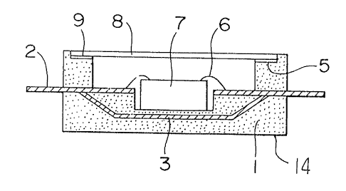
( Embodime:nt 1 )
In Fig. 1 which shows a side sectional view of an
example of a package for a semiconductor device in which an island
portion 3 is formed internally of a bottom surface, the reference
numeral 1 designates a hollow package made of synthetic resin, and
2, a lead frame.
8
2 0 4 l 4 8 ~ 72689-35
The island portion 3 is connected to the lead frame 2
through a support lead 3 and is situated in a lower position than
the remainder of the lead frame.
The reference numeral 4 designates a bonding surface on
which a semiconductor chip 7 is secured by means of adhesives, and
numeral 5 designates a cover adhesive portion for sealing a space
in the package.
The hollow package 1 is molded of resins as
aforementioned such as epoxy resin, polyamide resin.
in The lead frame 2 (including the island portion 3) is
formed of a material as aforementioned, preferably 42 alloy or a
copper alloy.
Other plate-like material such as a copper plate may be
joined to the island portion 3 for improving heat radiation
properties. In this manner, the plate-like member such as the
copper pl,~te which is joined to the island portion 3 provides not
only improved moisture impermeability of the semiconductor device
but also ;produces efficient radiation outside the package of heat
generated in the semiconductor chip 7 to maintain the stability of
2i) operation of the semiconductor chip 7.
The plate-like member may be of the same size as the
island portion 3, or may be of an area larger than the former.
In the present embodiment, the island portion 3 is
connected to the lead frame 2 through the support lead 3' as shown
in Fig. 4.
9
2 0 4 7 4 ~ ~ 72689-35
The island portion 3 is integrally formed in the same
plane as the lead frame 2 at the time of fabrication as part of
the lead frame 2. Thereafter the portion 3 is depressed out of
the plane of the lead frame 2 by suitable post-working.
By this means the island portion 3 and the lead frame 2
are formed of the same material. However, in order to improve
anticorrosion and radiation properties, the island portion 3 may
be partly plated, or another material such as a copper plate may
be joined to the island portion 3, as mentioned above.
As described above, the island portion 3 is preferably
formed inwardly (in the figure below the bonding surface 4) from
the bonding surface 4 and inwardly (in the figure, above the
bottom surface 14 of the package) from the bottom surface 14 of
the hollow package 1, particularly, closer to the bottom surface
14 by at least 100 um or more from the bonding surface.
The registration of the upper surface of the island
portion 3 with the bonding surface is not preferred since this
lowers moisture impermeability.
The position of the island portion 3 is suitably
adjusted .at the time the lead frame 2 is pressed, for example.
The thickness of the island portion 3 is normally 50 to
1000 um, ;preferably, 100 to 500 um, and is substantially the same
size as tine bottom surface of the semiconductor chip 7. A larger
sized island provides advantages in accordance with the
invention.
2 0 4 7 4 g 6 72689-35
The lid adhesive portion 5 is preferably provided with a
shoulder as shown in order to obtain better sealing effect.
The semiconductor chip 7 is secured to the bonding
surface 4 of the hollow package 1, the chip and the lead frame 2
are conne~~ted by a bonding wire 6, and thereafter the cover member
8 or lid is adhered to the cover adhesive portion 5 of the package
1 by adhesives such as epoxy group, imide group or acrylic group,
to provide an airtight seal.
The bonding wire 6 normally comprises gold or aluminum
1~) wire. The cover member 8 or lid may comprise a transparent cover
member 8 such as a glass plate, a sapphire plate, a transparent
alumina plate, a transparent plastic plate, etc., or translucent
or opaque cover members 8 such as a coloured glass plate, a
ceramics ;plate, a coloured plastic plate, etc.
While Fig. 2 shows an example in which the position of
the lower surface of the island. portion 3 is at the bottom surface
of the hollow package, the island portion 3 may be situated more
inwardly ~~f the bottom surface of the hollow package.
A semiconductor device according to this embodiment is
2~) manufactured in accordance with the following procedure.
The lead frame 2 having the island portion 3 depressed a
predetermined distance from other portions is initially set in a
predetermined position within the mold, and subsequently, epoxy
resin such as bisphenol A type, orthocresol novolak type, glycidyl
amine type, etc., is applied by injection or transfer molding.
11
2 ~ 4 7 4 8 6 72689-35
According to this method, the position of the island
portion 3 of the lead frame 2 sealed into the hollow package 1 is
fixed by depressing it using a suitable pressing means, for
example a press machine, so that its position is accurately
predetermined in advance. By this means the process involves a
single insertion step at the time of molding thus avoiding
difficulties of positioning.
The conditions of insert molding differ with use or
different kinds of resins. Where use is made of epoxy resin,
pressing and heating are carried out under the general conditions
of 10 to 800 kg/cm2 of pressure, 150 to 200 °C of temperature, 1
to 5 minutes of time, and post-curing is provided as needed. The
lead frame 2 having the depressed island portion 3 is subjected to
insert molding whereby the island portion 3 with excellent
moisture impermeability is secured with high precision to the
bottom surface of the hollow package 1 or to an inner portion
therefrom. Accordingly the operating steps are simplified, and in
addition, positive positioning can be attained.
The present inventors have conducted experiments as
2~D described hereafter in order to measure the level of moisture
impermeability of the semiconductor package according to the
present embodiment. In these experiments the entry of moisture
into the semiconductor package was tested in the following manner:
(Method A for evaluation)
A package sealed by a transparent cover member 8 Was
placed in a commercially available pressure cooker tester and
12
2 0 4 ~ 4 8 ~ 72689-35
heated and pressurized for two hours under the conditions of
temperature (121°C), humidity (100%RH) and gauge pressure
(1kg/cm2), after which it was removed. On the side of the
transparent cover member the package was pressed against the hot
plate and heated for 15 seconds at 80°C, and thereafter the
transparent cover member was pressed against a brass block for 10
seconds at 25°C to examine if condensation caused by moisture
which had entered was formed inside the transparent cover member.
Those which had no condensation indicated less entered moisture
1~D and were judged to present no practical problem. Accordingly, in
the present invention, the quality of the moisture impermeability
of the package is determined by the length of heating in the
pressure cooker tester time until condensation appears inside the
transparent cover material.
Experiment 1
A lead frame 2 (thickness:u250 m) made of 42 alloy
subjected to nickel plating with a lustering agent (saccharin)
combined having an island portion 3 as shown in Fig. 4 was
pressmold~ed. Only the island portion 3 was depressed and set to a
20 predetermined position within the mold of a transfer molding
machine.
Next, molding material of an orthocresol novolak type
epoxy resin and phenol novolak curing agent was transferred into
the mold 'under the conditions of 180°C temperature, 120 kg/cm2
pressure and 3 minutes time after which it was subjected to post-
curing for three hours at 180°C to obtain a molded article
13
2 0 4 7 4 8 6 X2689-35
(thickness of bottom is 1 mm) as shown in Fig. 1. Subsequently,
the cover adhesive portion 5 was coated with epoxy resin to form
an adhesive layer 9, to which a cover member 8 made from a
transparent glass plate was adhered to seal hollow package 1 in an
airtight manner. This hollow package 1 was tested in a pressure
cooker tester under the above mentioned conditions. The package
was removed every two hours to examine if condensation appeared on
the inside of the glass cover member 8.
As the result, no condensation was observed until 12
hours but condensation was recagnized first after 14 hours. The
results obtained by measuring the difference of moisture
impermeability as a result of varying the distance between the
package die pad surface (bonding surface 4) and the upper surface
of the island portion 3 is indicated by the curve (dotted line
marked by D) in Fig. 5. The thickness of the package used (from
the bottom surface of the semiconductor chip 7 (bonding surface)
to the bottom surface of the package) was lmm. The time until a
blur occurs inside was measured by the same method.
On the other hand, in. a package fabricated in the
2~0 exactly same manner except that. an island portion is not
incorporated, condensation was recognized in four hours by a
similar pressure cooker test.
Experiment 2
An experiment was conducted in a manner similar to that
of the aforesaid Experiment 1 except that nickelplated 42 alloy
was used without combination with a lustering agent, as the lead
14
2047486
frame 2.
726$9-35
The result obtained by measuring the difference of
moisture impermeability while varying the distance (t) from the
bonding surface 4 to the upper surface of the island portion, is
shown by the curve (solid line marked by ~) in Fig. 5.
It has been found frc>m the aforesaid results that the
preferred position for the island portion 3 is at an inner
position from the bonding surface 4, and internally of the bottom
surface of the hollow package 1., particularly, closer to the
bottom surface by at least 100 um or more than from the bonding
surface .
Experiment 3
An experiment was conducted in a manner similar to that
of the aforesaid Experiment 1 except that 42 alloy without applied
plating was used as the lead frame. As a result, the same result
as the curve marked ~ in Fig. 5, was obtained.
(Embodiment 2)
In this embodiment, a moisture-proof plate 11 separate
from a lead frame 2 is embedded. inwardly from the bottom surface
2~0 14 of the hollow package 1 as shown in Fig. 6.
In Fig. 6. the reference numeral 1 designates a hollow
package formed of thermosetting resins such as epoxy resin,
polyimide resin: 2, a lead frame formed of 42 alloy, copper alloy,
etc.: 4, ,a bonding surface for securing a semiconductor chip: and
5, a cover adhesive portion for sealing a semiconductor device,
the cover adhesive portion being provided with a shoulder for
~ 4 7 4 ~ ~ 72689-35
providing better seal effect similarly to the aforementioned
Embodiment 1. The reference numeral 11 designates a moisture
proof plate which is composed of material selected from the
aforementioned materials.
Where alloys or their oxides which have a heat transfer
rate in excess of 0.01 cal/cm. sec. °C are used, not only is the
moisture impermeability improved but radiation of heat generated
by the semiconductor chip 7 is promoted to provide operating
stability of the semiconductor element.
The thickness of the moistureproof plate 11 is normally
50 to 1000 um, preferably, 100 to 500 pm.
The size of the moistureproof plate 11 which is
positioned between the bottom :surface of the semiconductor chip 7
and the bottom surface of the hollow package, is preferably, as
shown in Fig. 6, substantially the same as the bottom surface
(lowermost surface) of the hollow package 1.
Preferably, the moist:ureproof plate 11 is embedded at
the bottom surface 14 of the hallow package 1 or inwardly thereof
as shown in Fig. 6. Where it i.s desired to enhance its function
as a radiation plate the moistureproof plate 11 may be situated
closer to the semiconductor chip 7 (for example, by adjusting the
length of a lead member 10).
Furthermore, as shown in Fig. 7 there may be provided a
lead member 10 positioned directly below the bonding surface 4 and
connected to the moistureproof plate 11. The lead member 10 is
preferably formed of a material having a heat transfer rate in
16
72689-35
2047486
excess of 0.01 cal/cm sec °C. With the provision of the lead
member 10, heat generated by the semiconductor chip 7 is
transmitted to the moistureproof plate 11 to enhance the radiation
effect.
In the manufacture of: the device lead frame 2 made of 42
alloy and a moistureproof plate 11 made of copper alloy having a
thickness of 250 um and a heat transfer rate of 0.53 cal/cm. sec.
°C, were inserted in predetermined positions within a mold of a
1D transfer molding machine. Next;, a molding material consisting of
a novolak type epoxy resin together with curing agent was insert-
molded at a temperature of 180oC, a pressure of 80 kg/cm2 and a
time of 2 seconds. Following which the molded material was
subjected to post-curing for 3 hours at a temperature of 180°C to
obtain a hollow package 1 as shown in Fig. 6. A cover member 8
made from a transparent glass plate was then adhered to the cover
adhesive portion 5 of the hollow package 1 by an epoxy resin
(adhesive layer 9).
The aforementioned insert molding conditions will differ
20 with the type of resin used. However, with use of epoxy resin,
the preferred heat and pressure conditions comprise a pressure of
to 500kg/cm2 temperature of 150 to 200 oC, and time of 1 to 5
minutes.
The moistureproof plate 11 is subjected to insert
molding simultaneously with the lead frame 2 to thereby fix the
moistureproof plate il at the bottom surface of the hollow package
17
2047486 72689-35
1 or inwardly therefrom, with high precision. Not only does this
simplify this assembly step but: it also accurately fixes the
position of the moistureproof x>late 11 as compared with methods by
which the moistureproof plate is adhered.
The airtight sealed package was evaluated under the
following conditions (Meth.od B for evaluation). The package was
subjected to a pressure cooker tester, to a temperature of 121°C,
humidity of 100%RH and gauge pressure of 1kg/cm2. It was removed
every 5 hours and was left. under room temperatures for an hour to
examine if condensation is observed internally of the glass cover
at room temperature. In evaluation Method B this package was not
cooled by use of temperatures other than room temperatures as it
was at this stage, in evaluation Method A.
As the result, condensation was not observed until 45
hours but recognized first. after 50 hours. By contrast, in a
package fabricated in a similar manner except that a moisture-
proof plate is not incorporated, condensation was recognized in 20
hours using a similar pressure cooker test. Thus the effect of
the moistureproof plate was conspicuous.
Thus, according to the present embodiment, the formation
of a layer consisting of a vapour-impermeable moistureproof plate
11 on the bottom surface of the: hollow package 11 or inwardly
therefrom, serves as a barrier against entry of moisture from the
bottom surface of the package where a moisture permeability into
the semiconductor package is normally highest. Furthermore, by
insert molding of the moistureproof plate 11 along with the lead
18
2 0 4 7 4 8 6 72689-35
frame 2, the moistureproof plate 11 can be fixed to the inner
surface or outer surface of the hollow package 1 with high
precision and by simple procedure.
The semiconductor chip 7 with which the invention may be
used may consist of a solid image pickup element such as Charge
Coupled Device, Metal Oxide Semiconductor or Charge Priming
Device. The chip is sealed by the above described hollow package
and the lid (cover member 8) i:c composed of a transparent glass.
When the invention is used with a solid image pickup
device, the device features airtightness, vaportightness and high
reliability.
19