Note: Descriptions are shown in the official language in which they were submitted.
2047502
SELECTIVELY PLATING ELECTRICALLY CONDUCTIVE PIN
This invention relates to selectively plated
electrically conductive pins and a selective plating
process for electrically conductive pins.
Conventionally, electrically conductive pins for
connectors and circuit boards providing gold contacts at
both ends have contact regions plated with contact gold, 30 -
100 micro inches thick, to provide good electrical contact
properties. A center portion of the pin may be plated with
o a thinner gold flash (3-10 micro inches), to provide
protection from corrosion and, in the case of a non -
compliant pin, to render the surface solderable.
Conventionally, the differential thickness of gold
plating on the end contact regions and on the center
portion of the pins is provided by electroplating from gold
plating solution in a controlled depth plating cell.
The center portion of the pin is generally in
contact with a printed circuit board with which it forms a
gas tight seal and which prevents deterioration.
Therefore, the central portion of the pin does not require
the special properties of a gold plating and a plating of
another, less expensive metal or alloy, such as tin-lead,
would be satisfactory. If pins are carried on a bandolier
during plating, gold which is incidentally deposited on the
bandolier during plating of the center portion of pins is
wasted unless the bandolier is processed after use to
reclaim the gold.
The present invention seeks to provide selectively
plated electrically conductive pins and a method for
selectively plating electrically conductive pins, which
avoids the above mentioned problems and allows the use of
less gold.
Thus according to one aspect of the present
invention there is provided a method of selectively plating
an electrically conductive pin having a center portion
between two end portions, the end portions having gold
plated contact regions, and the method comprising:
~~ ` ~
2047502
selectively masking desired gold plated contact regions by
coating one end portion of the pin with plating resist
material; plating the center portion of the pin with
another conductive material by controlled depth plating
with immersion of said resist coated one end portion and
center portion of the pin into a plating solution of said
conductive material; then after removal from the plating
solution removing the plating resist material from the pin;
whereby plating of the other conductive material over the
o desired gold plated contact regions is avoided.
In the method according to the latter aspect of
the invention, masking desired gold plated contact regions
protects the gold contact regions from contamination by the
other conductive material during plating of the other
conductive material on the unmasked pin surfaces. Also the
method according to this aspect ensures that gold plating
does not overlie the other conductive material.
Thus, the center portion of the pin is devoid of
gold and a plating of another conductive material is used
instead of gold on the center portion of the pin. The
method according to this aspect of the invention therefore
allows less gold to be used to provide a pin with a
conductive plating on end and center portions of the pin.
According to another aspect of the invention there
is provided a method of selectively plating an electrically
conductive pin having a center portion between two end
portions, the end portions having gold plated contact
regions, and the method comprising: selectively masking
desired gold plated contact regions by coating at least one
end portion of said two end portions with a plating resist
material; plating the center portion of the pin with a
layer of a controlled thickness of an other conductive
material during immersion of said resist coated at least
one end portion and the center portion of the pin in a
plating solution of the other conductive material; and,
after removal from the plating solution, removing the
plating resist material from the pin; whereby a layer of
3 204750~
the other conductive material is provided on the center
portion between gold plated contact regions of the two end
portions and plating of the other conductive material over
said desired gold plated contact regions is avoided.
s The step of masking desired gold plated contact
regions may comprise immersing said desired gold plated
contact regions of the pin in a liquid containing plating
resist material to provide a coating of plating resist
material. Preferably, the plating resist material is an
lo insulator and the coating of the plating resist material is
deposited from the liquid containing plating resist
material by electrophoresis.
In a convenient manner of performing the method,
one end portion of the pin is coated with plating resist
material to mask the gold plated contact regions on the end
portion, then, by controlled depth plating, electro-plating
the center portion of the pin with the other conductive
material. The masked end portion and center portion only
of the pin are immersed into a plating solution of the
other conductive material during the controlled depth
plating. The resist material is removed from the pin after
removal of the pin from the plating solution.
According to another aspect of the present
invention there is provided a method of selectively plating
a series of electrically conductive pins carried on a
bandolier, each pin having a center portion between two end
portions, and end portions only of each pin having gold
plated contact regions, the method comprising: moving the
bandolier along a passline and sequentially processing pins
30 as the series of pins move on the bandolier along the
passline, by steps including: selectively masking desired
gold plated contact regions with a coating of a plating
resist material; plating with another conductive material
the center portion of each resist coated pin; and then
removing plating resist material from pins, whereby plating
of the other conductive material over the desired gold
plated contact regions is avoided.
2047502
Thus, in a practical and advantageous method of
plating the pin, the pin is one of a series of pins carried
upon a bandolier. The bandolier is moved along a passline
to treat the pins in succession by selectively masking the
desired gold plated contact regions and then plating the
unmasked pin surface with the other conductive material.
According to yet another aspect of the invention
there is provided A method of selectively plating a series
of electrically conductive pins carried on a bandolier,
o each pin having a center portion between two end portions,
the method comprising: moving the bandolier along a
passline and sequentially processing pins as the series of
pins move on the bandolier along the passline, by steps
including; plating only end portions of the pins with gold
to form gold plated contact regions; selectively masking
desired gold plated contact regions with a coating of
plating resist material; plating the center portion of each
resist coated pin with another conductive material; and
then moving plating resist material from each pin, whereby
plating of the other conductive material over the desired
gold plated contact regions is avoided.
The method steps of selectively coating pins with
resist material and selectively metal plating the pins may
be carried out in a series of controlled depth processing
cells. Where pins are carried on a bandolier the process
may comprise an in line process where a bandolier carrying
pins moves along a passline from a supply reel to a take-up
reel as pins pass successively through the series of
controlled depth processing cells along the passline and in
30 which they are respectively resist coated, plated and
resist stripped.
Preferably the other conductive material comprises
a metal alloy having a low contact resistance, which may be
tin-lead. Where the electrically conductive pin is a non -
compliant pin, the other metal is preferably also asolderable metal alloy, i.e. tin-lead.
According to yet another aspect of the invention
5 ~75~2
there is provided a method of selectively plating pins
having a center portion between two end portions, the
method comprising: plating only end portions with gold to
form gold plated contact regions; selectively masking
desired gold plated contact regions with plating resist
material; plating the center portion of the pin with
another conductive material; and removing the plating
resist material, whereby an overlayer of gold on said other
conductive material is avoided.
lo According to a further aspect of the invention
there is provided an electrically conductive pin comprising
an integral body having a center portion between two end
portions; the pin body comprising an underplating on the
end portions and center portion, and the underplating
comprising a first conductive material other than gold;
and the end portions only being selectively plated
with gold to provide gold plated contact regions thereon,
the gold plated contact regions extending over the
underplating on end portions of the pin; ànd the center
portion of the pin being devoid of gold; and the center
portion of the pin being selectively plated with a uniform
thickness of an other conductive material, and the plating
of the other conductive material extending around the
center portion of the pin and over the underplating,
thereby covering the underplating on the center portion of
the pin; and the other conductive material contacting the
center portion only of the body and extending between gold
plated contact regions of the two end portions without
underlying said gold plated contact regions.
Thus the center portion of the pin is devoid of
gold and a plating of another conductive material is
provided on the center portion. Therefore a min;m~l amount
of gold is used, i.e. only on the end portions. The
structure of the pin may provide for the gold to overlap
the other conductive material so as that the pin is
completely plated and any under-plating on the pin is not
exposed.
~ ~ .
2047502
However, according to yet another aspect of the
invention there is provided an electrically conductive pin
comprising: an integral body having a center portion
between two end portions, and the end portions only being
selectively plated with a gold to provide gold plated
contact regions therein; and the center portion of the pin
being selectively plated overall with a uniform thickness
of an other conductive material; the other conductive
material contacting the center portion only of the body and
o extending between gold plated contact regions of the two
end portions without underlying said gold plated contact
regions, with inwardly facing surfaces of gold contacting
only the body of the pin; whereby an overlayer of gold on
said other conductive material is avoided.
In an advantageous structure of a pin according to
this other aspect invention the other conductive material
may overlap the gold plating, but the gold plating does not
overlap the other conductive material. This avoids a pin
structure in which the gold plating overlaps the other
conductive material. Such a structure could have problems
when the other conductive material is for example tin-lead,
which is softer than gold and does not provide a good base
for gold plating so that regions of gold overlying tin lead
may suffer wear in use and collapse. Preferably, the other
conductive material contacts gold plated contact regions
only at parts of the gold plated contact regions adjacent
the center portion of the pin, so that the gold plated
contact regions are not contaminated by the other
conductive material, which may lead to an increase in
contact resistance of the gold plated contact regions.
According to a further aspect of the invention
there is provided a series of electrically conductive pins
carried on a bandolier; each pin of the series comprising
an integral body having a center portion between two end
portions; the center portion of each pin being held by the
bandolier with said end portions of each pin extending to
opposite sides of the bandolier; the end portions only of
7 2047502
each pin being selectively plated with gold to provide gold
plated contact regions thereon; and the center portion of
each pin being selectively plated with a layer of a uniform
thickness of an other conductive material, and the
bandolier also being plated with said other conductive
material; the other conductive material contacting the
center portion only of each pin body and extending around
the center portion between gold plated contact regions of
the two end portions without underlying said gold plated
lo contact regions, and with inwardly facing surfaces of gold
contacting only the body of the pin, whereby an overlayer
of gold on said other conductive material is avoided.
Thus, the present invention provides a selectively
plated electrically conductive pin and a method of
selectively plating an electrically conductive pin having
end portions providing gold contact regions and center
portion plated with another conductive material so as to
reduce the amount of gold used for plating and to avoid the
above mentioned problems.
An embodiment of the invention will now be
described by way of example, with reference to the
accompanying drawings, in which:-
Figure 1 is a cross-sectional view along the
length of a electrically conductive pin of prior art
structure;
Figure 2 is a perspective view of the prior art
conductive pin of Figure 1 carried on a bandolier of prior
art structure;
Figure 3 a is a cross-sectional view of a
selectively plated electrically conductive pin according to
an embodiment of the present invention and Figures 3 b and
3 c are modifications of the pin of the embodiment of the
invention;
Figure 4 a - h is a schematic diagram of an
apparatus for in-line controlled depth plating of pins
according to the embodiment; and
Figure 5 a-c are cross-sectional views through
r~~`
2047502
pins at different stages in use of the process upon the
apparatus of Figure 4.
A prior art electrically conductive pin in the
form of a printed circuit board pin 10 is of conventional
structure for use with connectors and printed circuit
boards, as shown in Eigure 1, and comprises a body 11 of
rectangular cross section, having a phosphor bronze base
which is supplied pre-plated on two or four faces with a
nickel under-plating 18. End portions 12 and 14 of the pin
o body are selectively plated with gold to form gold plated
contact regions 13 and 15. The end portions 12, 14 of the
pins are of rectangular cross section. The gold plating on
contact regions 13, 15 of the end portions 12,14 may be
typically 30-100 micro inches in thickness and formed by
selective electroplating of each end portion 12, 14 of the
pin 10. A thinner plating of 3-10 micro inches of gold
plate (gold "flash") is provided on a center portion 16 of
the pin body 11. The center portion 16 of the pin body is
formed with a compliant section 17 for engagement with a
hole in a circuit board so as to form a contact. The pin
10 is one of a plurality of substantially identical pins
carried by a bandolier 20 as shown in Eigure 2, with end
portions 12, 14 of the pins extending each side of the
bandolier. The bandoliered pins are supplied on a reel
(not shown) to enable reel-to-reel processing of pins by a
continuous in-line process. The contact gold on the end
portions 12,14 and the gold flash on the center portion 16
of a pin may be provided by electroplating in conventional
controlled depth plating cells by immersing the center
30 portion and/or the end portions of the pin body to a
desired depth in gold plating solution. During plating of
the center portion 16 of a pin carried on a bandolier 20 ,
the bandolier incidentally receives a gold plating. To
prevent waste of gold, gold may later be reclaimed from the
3 5 bandolier.
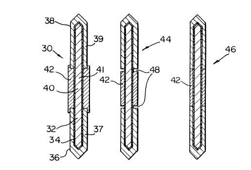
A pin 30 according to an embodiment of the present
invention is shown in Figure 3a. The pin is similar to
9 2047502
that shown in Eigure 1 comprising a body 32 having a
phosphor bronze base and including a nickel plating 34.
End portions 36 and 38 of the pin body are selectively
plated with gold to a thickness of between 30 and 100 micro
inches (i.e. 0.8 to 2.5~m) to form gold plated contact
regions 37,39. The pin 30 differs from the prior art pin
10 because a center portion 40, (the portion including the
compliant section 41) is selectively plated with another
conductive material, i.e. tin-lead alloy plating 42, and is
lo devoid of gold. The tin-lead alloy plating 42 on the
center portion 40 just overlaps the adjacent parts of the
gold plated contact regions 37,39 of the end portions 36
and 38, so that none of the nickel plated layer 34 of the
body 32 of the pin is exposed. Thus all inwardly facing
surfaces of the gold plated regions 37, 39 contact only the
end portions 36 and 38 of the pin body, that is, in this
case, the nickel plating 34 on the pin body 32. The gold
plating does not overlap the tin-lead plated center portion
40 of the pin body.
In use of the pin, the tin-lead plating 42 on the
center portion 40-provides an electrically conductive
plating having a low contact resistance between the
compliant section 41 of the center portion 40 of the pin
and a pin receiving contact hole of a circuit board or
connector. The tin-lead plated center portion 42 also
provides a solderable surface where a soldered connection
is required. The center portion 40 is devoid of gold so
that a selectively plated pin according to the embodiment
requires use of less gold, while the plating of the other
conductive material on the center portion of the pin
provides desired electrical contact properties. This
structure of the embodiment has a further advantage in that
the pin avoids problems encountered when gold overlaps a
softer material, such as tin lead, which does not provide a
good base for gold plating and which, during use, tends to
collapse.
In modifications of the embodiment, now to be
lo 2047502
described, the same reference numerals are used for
features identical with or similar to those of the
embodiment.
In one modification of the pin of the embodiment,
shown in Figure 3b, a pin 44 has the tin lead plating 42 on
the center portion 40 just spaced apart from the parts of
the gold plated contact regions 37,39 adjacent the center
portion 40, leaving a slight gap with portions 48 of the
nickel plated layer 34 of the body exposed. This structure
o may be used in applications where corrosion of exposed
portions 48 in the gap between the gold and tin lead
platings is not a concern.
In applications where it is desirable that the pin
is completely plated so that the underplating of the body
of the pin, i.e. the nickel plating, is not exposed to
corrosion, a pin 46 which is another modification of the
pin of the embodiment, and as shown in Figure 3c, provides
tin lead alloy plating on the center portion which abuts
but does not overlap the gold plated contact regions 37, 39
on the end portions of the pin body.
In both of the above modifications, the whole of
the gold plated contact regions 37,39 are exposed and the
other conductive material, (i.e. the tin lead alloy) 42
does not overlap the gold plated contact regions 37,39.
In a method of forming a plurality of finished
pins 30 of the embodiment, the pins 30 are carried on a
bandolier 20, similarly as shown for prior art pins 10 in
Figure 2, with the center portion 40 of each pin held by
the bandolier 20 and with the end portions 36,38 of the
pins extending each side of the bandolier. The plating
process is carried out conveniently as an in-line process
for which the bandoliered pins 30 are supplied on a supply
reel 52 and the bandolier moved along a passline 50 from
the supply reel to a take-up reel 54 so that the pins are
successively processed through a sequence of process steps
as described below (Figure 4a). The pins 30 have a
rectangular cross section, as shown in Figure 2, and they
11 2047502
are supplied pre-plated on two or four faces with an under -
plating 34 of nickel. As each pin is fed by the bandolier
20 along the passline 50, the four faces of the end
portions 36 and 38 are selectively electroplated with gold
by a conventional plating method in two controlled depth
plating cells 56, 58 where each end portion 36,38
respectively is immersed to the required depth in a gold
plating solution 57 and plated with a desired thickness of
contact gold to form the gold plated contact regions 37,39
on end portions 36,38 of the pins (Figure 4 b). To plate
both end portions of each pin, the bandolier is inverted in
its passage between the plating cells 56 and 58 (Figure 4b
and 4c). The contact regions 37 and 39 are plated to their
required 30-100 micro inches in thickness to provide the
desired contact characteristics. The gold plated pin then
appears, in section, as shown in Figure 5a. Hence the
center portion 40 of each of the pins and the bandolier is
not gold plated, and after gold plating of the end contact
regions of the pins, the nickel plating 34 of each pin body
32 r~m~; n~ exposed on the center portion 40 of the pin
body.
One end portion 36 of each pin 30 is then coated
with a plating resist material 60 (Figure 5b) to mask
desired gold plated regions, which, in this case, is the
whole of the gold plated contact region 38 on the one end
portion 36 of the pin except for a narrow band of gold 61
adjacent to the center portion of the pin (Figure 5b). The
plating resist material is preferably an insulator, such as
an acrylic resin based material, suitable for deposition by
electrophoresis, for example, Selrex Electroclear 2000~,
manufactured by Enthone OMI Canada Ltd.
The coating of plating resist material on end
portions of the pins is deposited by electrophoresis during
immersion of end portions of the pins in a liquid 62
containing the plating resist material 60 and contained in
a cell 64 (Figure 4d).
The liquid 62 is an aqueous suspension of
r~c
12 2047502
colloidal particles of the resist material. The
electrophoresis method allows a resist coating of an
insulating material to be controllably and uniformly
deposited over pin surfaces to a desired thickness of
approximately 1 thousandth of an inch in a process
analogous to electroplating. The pins are coated by
immersion in liquid containing the plating resist material
to the required depth to form a masking layer of resist
over the desired gold plated contact regions. The process
lo may be carried out using a known controlled depth
processing cell 64, similar to those used for
electroplating of gold, holding the liquid 62 containing
the plating resist material. Thus the extent of masking of
desired gold plated contact regions is controlled by
controlling the depth of immersion of end portions of pins
into the liquid containing plating resist and a layer of
resist material is deposited to the desired thickness by
electrophoresis.
After the pins leave the cell 64, the plating
resist material is dried and partially cured by a
conventional method comprising exposure to infrared radiant
heat, or to hot air indicated at 66 in Figure 4e. The
resist material is preferably cured by air drying at 1-40F
for 1 minute. This results in an uncured or partially
cured material which has sufficient resistance to be
unaffected by subsequent acid cleaning and plating
operations and to prevent contamination of these solutions,
but lack of complete curing facilitates subsequent removal
of the material from the pins without trace of residual
contamination. This rapid curing process is in contrast to
the usual curing process used with Selrex Electroclear
2000~, for its conventional use for tarnish protection of
jewellery, where the resin coating is cured at 311F for 20
minutes. The latter process is unsuitable for the present
application.
After masking of desired gold plated regions of
one end portion of each pin, the pins are then selectively
204 7502
plated with the conductive material, i.e. a tin-lead alloy,
to provide the plating 42 (Figure 5c). This is performed
in another conventional controlled depth plating cell 68
(Figure 4f), one resist coated end portion 36 and center
portion 40 of each pin being immersed into the tin-lead
plating solution so that the exposed nickel plated region
and any unmasked gold plated contact region of this one end
of the pin is electro-plated with tin-lead (Figure 3c).
The bandolier is incidentally lead-tin plated too. The
0 pins are preferably immersed to a sufficient depth that the
tin lead plating 42 just overlaps the adjacent end 63 of
the gold plated contact region 39 at the other end portion
38 as shown in Figure 3a and 5c.
The plating resist material is then removed from
the pins by immersion of resist coated ends of the pins
into a hot alkali stripping solution, containing for
example potassium hydroxide and other water soluble
solvents such as butyl- and hexa-cellusolves, with
agitation, in another conventional reel-to-reel controlled
depth processing cell 70. The preferred stripping solution
is Cathoclear Stripper 200~ manufactured by Enthone OMI
Canada Ltd. Because the Electroclear 2000~ resin used as
resist material on the pins is not fully cured, the removal
of the resist material can be completed by two 10 second
dips, with vigorous agitation at 140F. Cathoclear
Stripper 200~ is the material normally used to clean
plating racks of cured Selrex Electroclear 2000~ resin
prior to re-use, by immersion for several hours at 140F,
but such an extended processing time is clearly impractical
30 for an in-line stripping process.
Gold, nickel and tin-lead plating are resistant to
immersion in the hot alkali stripping solution. It is
important in this application that traces of the masking
resin are removed from the gold surfaces. The selected
35 materials can accomplish this removal effectively by a
cascade arrangement of two or more stripping tanks. The
last stripping tank is the cleanest, supplying solution to
s'-
14 204750~
the first stripping tank which is then discarded after it
becomes too heavily loaded with resin.
Thus the desired gold plated contact regions are
masked by plating resist material during the tin-lead
plating process to prevent contamination of the gold plate
with tin-lead which may cause unacceptable increases in
contact resistance, i.e. 0.2mQ or more. The pin is
selectively plated with gold on the end portions and tin -
lead on the center portion.
lo In the above described method, the tin lead
overlaps the parts of the gold plated contact regions
adjacent the center portion of the pin to provide the
structure shown in Figure 3a. This has the advantage that
the pin is completely plated, but the gold does not overlap
the relatively soft tin lead. The nickel underplating is
completely covered to avoid exposure of nickel which may
result in corrosion and blackening, which, apart from being
visually unacceptable, may in use result in poor electrical
contact. Also, nickel may have a high contact resistance
with other metals at contact holes in circuit boards.
Further, by using the in-line process described, not only
is gold not used on the center portion 40 of each pin, but
also it is not used to plate the bandolier. Hence gold is
only applied in the locations where it is basically
required, i.e. at the end regions, 36 and 38.
In the manufacture of the modified pin (Figure
3c), in order to obtain a continuous plating, gold plated
contact regions on one end portion of each pins are
completely coated with resist material 50 without the
30 resist material extending onto the center portions 40 of
the pins. During plating of the tin-lead by the method
described for the embodiment, one end portion and the
center portion of the pin is immersed so that the tin-lead
plating extends only over the center portion of the pin, so
as to cover only the exposed nickel plated region of the
center portion of the pin, but the pin is not immersed
sufficiently for the tin lead to overlap gold plated
,~v~
2047502
contact regions at the other end portion of the pin. Thus
the pin is completely plated with gold on end portions and
tin lead over the center portion with the gold abutting the
tin lead, but not underlying or overlying it. Ideally the
depth of immersion of the end portions of the pins into the
plating resist material may be controlled so as to mask the
gold plated contact regions completely or partially.
However, this ideal situation is very difficult to control.
The other modified pin 44, (Figure 3b) is more
o practical to achieve wherein the resist material 50 is
caused to extend completely over the gold plated region 37
and slightly onto the center portion 40 of the pin. The
tin lead alloy plating does not extend onto the resist
material which, upon removal results in one portion 44 of
nickel being exposed. The other portion 44 is formed by
holding the gold plated region 39 spaced slightly above the
liquid 62 containing plating resist material 60 in cell 64
(Figure 4d).
Thus, by selectively masking desired portions of
the pin, i.e. the whole or part of the gold plated end
portions with plating resist material, pins having
different regions selectively plated with one or more
metals may be produced, with or without overlap between the
different metals.
In a modification of the process of the
embodiment, pins may be provided with gold plating on only
two of four faces of end portions of the pins by gold
plating in a mechanical masking type plating cell.
In an alternative method of providing any of the
30 pins of Figures 3a, b and c, desired gold plated contact
regions of both end portions of a pin are masked with
resist and the center portion of the pin is plated with
another conductive material. This method provides the
advantage that resist coating on the other end portion of
the pin ensures that gold plated contact regions at both
ends of the pins are protected from contamination by the
other conductive material. For example, accidental
16 2047502
immersion of ends of pins to a greater depth than desired
may result in excessive overlap of the other conductive
material on desired gold plated contact regions which may
be avoided by resist coating both end portions of the pin.
Electrophoresis coating with Electroclear 2000
material provides a continuous and uniform coating in
contrast to conventional plating resist materials and
methods, which were found to be unsuitable for the present
application. Eurthermore, electrophoresis provides rapid
o deposition of resist material with immersion times of less
than l minute per pin which is acceptable for an in-line
process. However, the curing and stripping processes used
in the present application are completely different from
the conventional use of electrophoretically deposited
Electroclear 2000~ material which required extended times
for curing and stripping processes. The latter processes
are therefore unsuitable for rapid in-line processing. In
the present application, a completely different process
results in a partially cured resist material which may be
easily and rapidly stripped, by immersion of the pin in a
stripping solution for only 10 to 20 seconds, without
leaving residue or contaminants on gold plated contact
regions, thus resulting in higher yield of pins with
desired electrical contact properties. Eurther, the use of
an aqueous system avoids problems with environmental
contamination, flammability and disposal of conventional
plating resist materials, such as solvent based solutions
of varnishes or wax, and reduces the use of stripping
solutions of organic solvents, including chlorinated
3 o solvents.