Note: Descriptions are shown in the official language in which they were submitted.
89-3-705 -1-
METHOD OF DEPOSITING FLUORINATED SILICON NIT~IDE
This invention relates to methods of producing semi-
conductor devices. More particularly, it is concerned
with methods of depositing silicon nitride films on sub-
strates in the manufacturing of semiconductor devices.
Silicon nitride films are widely used in the manufac-
ture of semiconductor devices and integrated circuits.
Plasma deposition of silicon nitride is a relatively low
temperature process which is used frequently so as not to
10 cause harmful effects to previously fabricated device
structures. Such a process is particularly desirable for
the deposition of final passivating films for protecting
the device surfaces.
In the past silicon nitride films have been plasma
deposited by employing a gaseous mixture of silane and
ammonia together with a suitable carrier gas such as
argon, helium, or nitrogen and using a high frequency RF
plasma. High frequency RF plasma techniques frequently
produce a deposited film which is under tensile stress
causing cracks in the film upon subsequent high
temperature manufacturing operations. Films deposited by
this method may also contain impurities resulting from the
difficulty in purifying the ammonia reactant. In addition
ammonia/silane nitride films have a considerable amount of
hydrogen incorporated in the deposited film. When these
films are an integral part of the active device structure,
the incorporated hydrogen has been shown to be detrimental
to device stability. When these films are applied as the
final protective passivation layers on MOS devices, the
hydrogen atoms can diffuse into the gate oxide and create
traps for hot electrons.
Because of these problems, there have been efforts to
reduce the amount of hydrogen in plasma deposited silicon
nitride films. Nitrogen has been substituted for ammonia
as the nitrogen source during the deposition step. In
89-3-705 -2-
other efforts to reduce the concentration of hydrogen,
fluorine in the form of SiF4, NF3, or F2 has been
employed as a reactant in addition to the silane during
the deposition process. The purpose of the fluorine is to
replace relatively weak Si-H bonds with stronger Si-F
bonds to improve the deposited silicon nitride film. In
addition, efforts have been made to change the stress in
the deposited film from tensile to compressive by using
low frequency, typically below lMHz, rather than high
10 frequency RF for generating the plasma.
According to one aspect of the invention, there is
provided a method of depositing silicon nitride on a
substrate comprising: positioning an electrode having a
coating containing fluorine and silicon in a reaction
chamber; placing a substrate on a .support in said chamber;
introducing silane and nitrogen into said chamber; and
applying RF electrical energy between said electrode and ,~
said support to generate a reactive plasma within the
chamber and deposit fluorinated silicon nitride on said
substrate.
According to another aspect of the invention, there
is provided a method of depositing silicon nitride on a
substrate comprising: placing an electrode in a reaction
chamber; introducing carbon, fluorine, and oxygen into
said chamber; generating a reactive plasma within said
chamber; introducing silane and nitrogen into said
chamber; generating a reactive plasma within said chamber
to deposit a coating containing fluorine and silicon on
said electrode; placing a substrate on a support in said
chamber; introducing silane and nitrogen into said
chamber; and applying RF electrical energy between said
electrode and said support to generate a reactive plasma
within the chamber and deposit fluorinated silicon nitride
on said substrate.
'': ~' ' ' ''
89-3-705 -3-
Some embodiments of the invention will now be
described, by way of example, with reference to the
accompanying drawing in which:
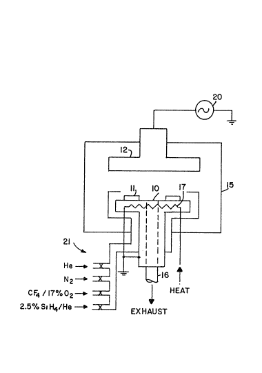
The sole figure is a schematic representation of
plasma deposition apparatus employed in carrying out the
method of the invention
For a better understanding of the present invention,
together with other and further objects, advantages, and
capabilities thereof, reference is made to the following
lO disclosure and appended claims in connection with the
above-described drawing.
In the following discussion the method in accordance
with the present invention is employed to deposit a fluor-
inated silicon nitride film as a protective passivation
layer on silicon wafers containing junction field effect
transistors.
A schematic representation of the apparatus employed
is illustrated in the sole figure of the drawing. The
20 apparatus is a conventional RF plasma deposition system.
Specifically, a Plasma-Therm PK1232 reactor which is
manufactured by Plasma-Therm Inc., Route 73, Kresson, NJ
08053. The apparatus includes a support 10 for substrates
11 to be treated and an elèctrode 12 positioned opposite
the support 10. The support 10 and electrode 12 are
typically of aluminum, are 10 inches in diameter, and are
spaced apart 0.7 inch under operating conditions. These
elements are positioned within a chamber 15 which can be
sealed. The chamber 15 is exhausted through an exhaust
30 port 16 centrally of the support 10. Reactant gases are
admitted at the periphery of the upper surface of the
support 10 by way of inlets 21. A heating element 17 is
mounted within the support 10 for heating the substrate
11. An RF generator 20 provides RF energy between the
electrode 12 and support 10 to form a reactive plasma
within the chamber 15.
89-3-705 -4-
Prior to placlng the substrate 11 which is to be
coated with a silicon nitride film in the apparatus, the
electrode 12 is prepared by forming a coating containing
fluorine and silicon, specifically ammonium hexafluoro-
silicate, on the surface of the electrode 12 facing the
substrate support 10. A mixture of carbon tetrafluoride
and o~ygen, CF4\17%02, is introduced into the chamber 15
at a rate of 100 cc per minute. The pressure within the
chamber is rçduced to 400 millitorr, the support 10 is
lO heated to 350C, and RF energy of 275 watts at 100 KHz is
applied to form a reactive plasma. This treatment is
maintained for 1 hr and introduces a large quantity of
fluorine into the system. Next, nitrogen, N2, is intro-
duced at a rate of 200 cc per minute with the pressure
maintained at 900 millitorr, the temperature at 350C, and
RF energy of 115 watts for a period of 1 hr. This proce-
dure reduces the residual oxygen left from the presence of
oxygen in the previous step and removes some of the excess
fluorine.
In order to remove gaseous materials from the
chamber, helium is admitted at a rate of 500 cc per minute
under a pressure of 900 millitorr and support temperature
of 350C for 15 minutes. After this cleaning step, a
mixture of silane and helium which is 2.5% SiH4\He is
admitted to the chamber at a rate of 100 cc per minute
together with nitrogen, N2, at a rate of 200 cc per
minute. Thus providing a ratio of 2.5 cc SiH4/200 cc N2
or .012 SiH4/N2 parts per volume of silane with respect to
nitrogen. The -pressure is 900 millitorr and the
30 temperature is 350C. A plasma is formed by applying RF
energy of 50 watts at 100 KHz for a period of 15 minutes.
Subsequent to this treatment, the chamber is flushed with
helium at a rate of flow of 500 cc per minute at a
pressure of 900 millitorr and temperature of 350C for a
period of 1 hr.
89-3~705 -5-
As a result of the foregoing procedures the electrode
12 and also the support 10 are coated with material con-
taining fluorine and silicon, specifically ammonium hexa-
fluorosilicate. This material serves as a source of
fluorine during subsequent plasma deposition of silicon
nitride on substrate wafers.
In the process of depositing silicon nitride films
one or more substrates 11 which may be wafers of silicon
of standard 3 inch diameter are placed on the support 10.
Specifically, the wafers may incorporate junction field
effect transistors of the static induction type which are
to receive a final protective passivation film of silicon
nitride. The pressure within the chamber 15 is reduced to
20 millitorr and the temperature of the support 10 is
maintained at 350C for 1 minute. Helium is introduced at
a rate of 500 cc per minute at a pressure of 250 millitorr
and the temperature is maintained at 350C for 1 minute.
The steps of reducing the pressure to 20 millitorr and
introducing helium at a rate of 500 cc per minute at 250
20 millitorr is repeated two more times. Then, the pressure
within the chamber is reduced to 20 millitorr and main-
tained at that pressure for 5 minutes with the temperature
at 350C. The foregoing procedure removes water vapor
from the system in preparation for the deposition of
silicon nitride.
A mixture of silane and helium, 2.5% SiH4\He is
introduced at a rate of 100 cc per minute and nitrogen,
N2, is introduced at a rate of 200 cc per minute. The
pressure is maintained at 900 millitorr and the
30 temperature at 350C. RF energy of 50 watts is applied at
a freguency of 100 KHz. Under these conditions silicon
nitride deposits on the upper surfaces of the substrate at
the rate of 60 Angstroms per minute.
Analysis of deposited silicon nitride films has shown
the presence of fluorine in amounts of between 6 and 8
atomic percent. The fluorine atoms are uniformly
, . .
- . - ~ , .
89-3-705 -6-
distributed throughout the film. The deposited films are
of uniform thickness within 2 to 5%, both from wafer to
wafer within the same run and from run to run. The fluor-
inated silicon nitride films are compressively stressed
and remain free of cracks after subsequent high
temperature treatment. In addition, pinhole densities in
the films are low and the films provide excellent step
coverage on uneven substrate surfaces. Furthermore, the
resulting fluorinated silicon nitride films are readily
10 etched either by employing conventional plasma or chemical
etching procedures.
While there has been shown and described what is
considered a preferred embodiment of the present
invention, it will be obvious to those skilled in the art
that various changes and modifications may be made therein
without departing from the invention as defined by the
appended claims.