Note: Descriptions are shown in the official language in which they were submitted.
lNTEGR~l[ED MAGNETIC READ/WRITE
HEAD/FLEXURE/CONDUCTOR STRUCTURE
Background and Summ~arv of the Invention
This invention relates to an electromagneti~ read/write structure for the
reading and writing of magnetic images on a relatively movin'g rnagnetic recording
medium. More specifically, it relates to a unique, unitary, integrated read/write
head/flexure/conductor structure of extremely small size, and to a method of rrlaking
the same. In characterizing the size of the proposed structure, I think of the same as
a micro flexhead. , ~- `
While the structure of the invention may be used in a wide variety of
applications, a preferred embodiment of the same is described herein in conjlmction
with reading and writing images with respect to rigid recording media, such as a disk ~- -
or drum, in which application it has been found to have particular utility and to offer
: `
special advantages.
The performance of magnetic recording systems improves rapidly as the
separation between the read/write head and the associated recording medium -
decreases. In rigid media systems, today, this separation is referred to as "flying
height"--a re~erence relating to the fact that the conventional head, often referred to
as a slider, is supported above the relatively moving medium surface by an air
20 bearing. As the flying height is reduced, the risk of head wear, and in particular the
potential for catastrophic wear or head "crash", increases rapidly. This problem may,
, . . .
of course, be minimized by proper selection of slider and medium surface materials
relating to hardness, coefficient of friction, thermal conductivi~r, etc., and also by ~ :
paying proper attention to the quality of the head/media interface, lubrication and the : -
elimination of contaminants which may appear in that interface. `~
Nonetheless, in a typical system of this type currently, the head structure ; ~ - -
. .
contacts the moving medium in the start and stop process, and occasionally in the
operating mode, resulting, inevitably, in some degree of abrasive if not catastrophic ~ -
wear. In general, wear rate is dependent upon surface velocity and applied pressure
and, for a given velocity, increases slowly with pressure. However, at some point the
wear rate rises steeply, resulting in some form of catastrophic wear.
One difficulty in understanding the wear process and in limiting wear,
particularly in low flying heads on rigid media, is that the area of contact is
irequently orders of magnitude smaller than that of the "footprint" of the slider. This
is due to one or more of a variety of factors, such as roll and pitch dynamics, or the
presence of a foreign particle in the head/medium interface. As a consequence, the
transient local contact pressure, resulting from applied load plus inertial forces, may
10 become extremely large. Looking at this situation a bit more closely, a key point is
that such microscopic regions of contact are largely independent of the size and mass
: ~ .
of the slider and, since reduction of the size and mass of the slider enables a
,
corresponding reduction in the applied load and inertial forces, local contact pressure
may be reduced accordingly. -- ~ -
Another reason for reducing the footprin~ of a slider as head/medium
. . . . .
separation is reduced relates to the fact that slider roll or non-flatness of the medium
or slider surface may cause the tip of the read/write pole to be abnormally separated ~ -
from the medium. ; - ~
.. .......
Reducing the size, mass and applied load of a slider, of course, requires ;~- ~
appropriate attention to the design of the air bearing of the slider, namely, a - -
~~: - . .
reduction of the slider's surface corresponding to the reduced applied load, in order - -
to maintain the desired flying height. Also to be noted is the fact that the constraint
on size and mass reduction of a slider with conventional designs lies in the practical
limitations of fabricating slider bodies, air bearing rails and gimble-flexures
mechanisms with appropriately small dimensions and tolerances, and mounting the :-;
sliders on !~exures with correspondingly tight tolerances. Ultimately, the minimum size : i
and mass is determined by the dimensions of the transducer, electrical conductors and ,~ -
,. . .
supporting structure. Present sliders are one to two orders of magnitude larger in
2 ~-
'. :
. .
2 a ~ 7 ~ 6 3 CNR 309Cl
size than the transducer itself, and as much as thrce orders o~ -
magnitude larger ln mass. Thus, in principle, the mass, and '~
therefore the local contact pressure, could potentially be
reduced by about three orders oE magnitude, thereby yreatly '--~
reducing abrasive wear, and perhaps also eliminating the
possibility of a head crash.
In summary, major advances in the performance of
medium magnetic recording systems may be achieved by Eurther
reducing head/medium separation-ultimately to continuous -
sliding contact. However, reducing head/medium separation,
other things being the same, results in an increased abrasive
wear, and in a greater risk oE catastrophic wear. Since the
area of contact between a slider and a medium is typically very
small and relatively independent of the slider's
macrodimensions, it should be possible to reduce greatly the
size and mass of the slider, thus to enable a corresponding
reduction in the applied and inertial forces and the local
contact pressure, all resulting in greatly reduced abrasive
wear and lower risk of catastrophic wear. Reduced footprint ~-
dimensions of a slider would also help to maintain small
separation between the head and medium.
;r. ~
The present invention provides a multistage method of
making an integrated, unitary read/write head/flexure/conductor
structure for the reading and writing of information with ~ -
.. ~. :: ,
respect to a relatively moving recording medium, such as a disk -
or drum, said method comprising, forming in plural stages, and
by a deposition process, an elongate dielectric flexure body -~
having a width dimension defined by a pair oE etch-removable,
. . .
wall-like stripes, and during said forming, creating within ~
30 ~such body in plural stages which are interspersed with said - -
. .
forming stages, and also by a deposition process, magnetic :
'. , :- , .
:~ . ', - .
A~ .: .. . . - -
`.
.. ..
2 ~ ~ 7 ~ ~ 3 240~7-579
CNR 309Cl
read/write pole structure having components formed generally
via deposition steps which are orthogonally-differentia~ed with
respect to each other, and electrical coil and conductor means
, . - :.. . .
operatively associated with such pole structure.
The invention also provides a method of making an
integrated, unitary read/write head/flexure/conductor structure
for the reading and writing of information with respect to a
:. -
relatively moving recording medium, said method comprising, ~
forming on a first planar surface of a nonmagnetic host wafer, ~ - -
by a deposition process, and in plural stages, an elongate, -
dielectrie flexure body, and during said forming, creating
. .
within sueh body, ln plural stages whieh are interspersecl with
the forming stages, and also by a deposition proeess, magnetic
yoke strueture, and an eleetrieal eoil and eonductor means
: - . . ..
operatively assoeiated with sueh yoke structure, exposing an
end surfaee of sueh body and yoke structure in a newly formed ~
,.- -: . - -:
seeond planar surfaee whieh is generally orthogonal to such -
.:: :: ..:
first planar surfaee, and fabrieating on sueh seeond planar ~ -
surfaee, by a deposition proeess, a pole strueture magnetieally ~ -
: ;, ~ - . .
eoupled to and operatively assoeiated with sueh yolce strueture. ~ ; -
The invention further provides a method of making on
a supportlng substrate an integrated unitary, read/write - ~
head/flexure/eonduetor strueture for the reading and writing of -
:, : ; ,: .
;~ information with respeet to a relatively moving reeording
medium, said method eomprising, preparing, on a surfaee in sueh -
a substrate, an etehable layer, forming on sueh layer in plural
,.. . .
stages, and by a deposition process, an elongate, dielectrie
flexure body whose width is defined by etehable wall-like
stripes that extend on the layer along opposite sides of the
~30 ~ body, with sueh stripes being etehable under the same - ; :
~eireumstanees that sueh layer is etehable, ereating within sueh
4 ~ -
.. ~ . , ,; .. . .
- ., :. . .: .
.-''` :'':-:'' -'
2 ~ ~ 7 a ~ ~ 24047-579
body, in plural stages whictl are interspersed with the forming
stages, and also by a deposition process, magnetic read/write
pole structure, and electrical coil and conductor means
operatively associated with such pole structure, and Eollowing
said preparing, forming and creating, etching such layer and
such stripes to free the body from the substrate.
The invention still further provides a method of
making plural, integrated, unitary read/write :
head/flexure/conductor structures each Eor the reading and
writing of information with respect to a relatively moving
recording medium, said method comprising, forming in plural
stages, and by a deposition process, plural, side-by-side
adjacent, elongate, dielectric flexure bodies whose respective
widths are defined by etchable wall-like stripes that extend -
between and separate adjacent bodies, creating within each such
body, in plural stages interspersed with the forming stages,
and also by a deposition process, magnetic read/write pole
structure, and electrical coil and conductor means opeL-atively ~ -
associated with such pole structure, and following said forming
and creating, etching such stripes as a step toward freelng
individual bodies.
By means of the invention it becomes possible to ~-
provide a unique read/write structure, which is orders of ~
magnitude smaller in si~e and mass when compared with today's ~ ;
counterparts--a structure which is capable of non-catastrophic, ;~
continuous sliding contact interaction with the surface of a -
relatively moving recordlng medium. A unitary and totally
. :.
integrated head~flexure/electrical conductor combination can be :-
formed entirely, atom-by-atom, in a deposition process, e.g. by -~
.- - .-: - . -
sputtering and photolithographic patterning of materials. The
structure easily allows for multiple-head arrays. ~ -
4a
.';'~':`',~
2~ 3~ ~
2~0~7-579
CNR 309Cl
Formlng diEferent portions o~ the necessary magnetic
substructure within the overall str~cture on generally
orthogonally related planes, permits very precise, small- .
dimens.ion, dimensional control. A readily etchable structure-
supporting base layer, as well as readily commonly etchable ~.;
boundary walls, positioned between adjacent flexure structures .~.
during the manufacture of plural structures can be formed to . .
promote, cooperatively, greatly simplified ultimate separation - ~
(singulation) of individual flexures. ..
These and other advantages which are attained by the
invention will become more fully apparent as the description - :.
which now follows is read in conjunction with the accompanying
drawings. .
: .,... .. -
Descri~tion of the Drawinqs
Figure 1 is a working-side perspective tslightly . `: .-
rotated) view of a read/write structure constructed in . ~ .
accordance with the present invention. ~ ~ .
Figure 2 is an enlarged longitudinal lateral cross - ~:.. -
section of the structure of Figure 1 illustrating the ~: -
integration therein of a probe-type head (transducer), an ~ .
electrical coil and conductive traces connecting therewith, and
an embedding flexure body. ~ :~
Figure 3 is a plan view taken generally Erom the
bottom side oE Figure 2,
Figure 4 is a simplified view illustrating the ..
magnetic interaction which occurs between the head in the . :
structure of Figures 1, 2 and 3 and magnetic layers oE an . . ~;
~ associated, relatively moving, rigid recording medium (disk).
;~ Figure 5 is a fragmentary view, somewhat like that oE - :.
. Figure 2, illustrating an alternative construction which
,'; .- :' : ,
~';'.~'` '
:.~ 4b
.,:, - .'. ,. ' :
'~'': .,~ -,' ~, ' ..
, : . ~ : . .
240~7-579
~ V ~ 3 CNR 309Cl
includes a ring-type read/write head (transducer).
Figures 6-13, inclusiver illustrate steps in the
manufacture of the structure
, .
.. ...
-...'' :
': '.:: ~.. . ' '
~' -.-' :
i ,~
i . .: .
' : .-:'' .:
: .
:,. . -,
,;:
.::
. . : -:
: . . - .
: - : . -
..: . ~
: 4c
. .~ . .. , :
'' -;. '- ~ :: .
:' :
of Figs. 1, 2 and 3.
Fig. 14 (plate 2) is a fragmentary perspective (non-working side) view of
a multiunit array of structures like the one shown in Fig. 1.
Dçtailed Description of the Invention
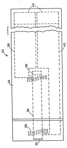
Turning now to the drawings, and referring first of all to Fig. 1,
, ... . . .
indicated generally at 20, is a read/write head/flexure/conductor stru~ture constructed ~ -
in accordance with the present invention. Structure 20 herein has an overall length A
of about 0.3-inches~ and overall width B of about 0.006-inches, a thickness C along
most of its length of about 0.001-inches, and a somewhat greater thickness D of about
0.002-inches forming an enlargement adjacent its left end in Fig. 1, which end may be
thought of as the read/write working end of the structure.
The particular dimensions just given have been chosen because they
work particularly well. However, I recognize that different specific dimensions,
preferably generally near the ranges set ~orth below, can be used quite successfully.
A- 0.2 - 0.5-inches
B - 4 - 20-mils
C- 15 - 60-microns
D - 20 - 65-microns
Considering Figs. 2 and 3 along with Fig. 1, the read/write structure now
.. ,: ,. -
being described is ~ormed with a probe-~pe head for perpendicular recording, with `- ;
this head including a main pole 22, a yoke 24, a back-gap stud 26, and a flux-return
yoke 28. These components are magnetically coupled to form a low-reluctance path,
terminating in a high-reluctance gap 30 between main pole æ and the end of return -
yoke 28. This return yoke may be made preferably somewhat wider than yoke 24 to -
provide a very large area of flux-coupling and a low-reluctance path to the soft
magnetic underlayer of the recording medium.
In the structure which has just generally been described, the lateral
dimension (the left-to-right dimension) of main pole æ as seen in Fig. 2 is preferably
extremely small, lying, for example, within the range of about 0.1- to about 3.5-
m;crons. With respect to this dimens;onal matter, an ;mportant component of the
method of mamlfacture d;sclosed here;n is that ma;n pole 22 ;s formed on and along
a plane wh;ch ;s substantially orthogonal relat;ve to the plane on and along which ;
yoke 24, ;ts compan;on in the pole structure, is formed. What is especially significant
is that, by employing deposition steps on such an orthogonal plane, relative to the
plane on wh;ch yoke 24 is formed, it is extremely simple to control, accurately, the
vely small main pole dimension which has just been referred to above. Control ofthis d;mension would be very difficult if one were to attempt to form main pole 22 by
depos;t;on occurring from the top-side direction of the structure as shown ;n Fig. 2. `:
With reference for a moment to Fig. 4, such a medium is shown
generally at 32 ;nclud;ng the just-referred-to soft magnetic underlayer 32_ covered
with a high-coercivity, perpendicularly oriented recording layer 32k. The direction of ~;
motion o~ medium 32 relative to the head is indicated by arrow 31.
The magnetic pole structure just generally described is formed in a
manner which will be further outlined later as a structure embedded within an `
elongate, dielectric flexure body 34 wh;ch ;s made herein, for example, of alununum
oxide. Other flexure-body materials, such as silicon dioxide, may also be used.
Induct;vely coupled to yoke 24 ;n structure 20 ;s a helix coil 36, also
formed in a manner which will be described shortly, with the ends of this coil ; ~
connectlng through lead conductors 38, 40 to bonding pads 42. - ~ -
Shifting attent;on for a moment to Fig. 5, here there is shown an
alternative embodiment of the invention, wherein structure 20 includes a forrn of th;n ;
film, ring-type head for recording on longitudinally oriented media, i.e., with an easy `. ~
.-
axis of magnetization in this plane of the media. In the structure there are included ~ -
poles 44, 46 which are relatively thick (in order to avoid pole tip saturation) with ` ~ ~ -
their lower extrernities substantially coplanar so as to be in close prox;m;ty to the ~ ~;
surface of an underlying recording medium. ` -
'. ~. .', .
6 `
, . . .
' ' '
Gap 48 which exists between these poles is made very small in order to
afford good linear bit resolution in signal reproduction. It is this dimension which
determines the linear bit resolution in signal reproduction. Most of the flux, produced
by current flow in the helix coil, bridges directly across gap 48, with only a small part
fringing out to the medium, thus limiting the field intensity in the record mode. For
this reason, it is necessary to restrict the throat height of gap 48 (the space where
poles M, 46 confront and parallel one another) so as to cause more of the flux to
encompass the medium. As a rule of thumb for thin-film, ring-type heads, the throat
height is held to one or two times the gap thickness in order to provide sufficiently
10 high field intensity for recording on high coercivity media. Thus, in current thin-film
longitudinal recording heads, gap 48 may be about 0.5-micrometers, thereby enabling
linear bit resolution of about 20,000-flux-reversals-per-inch, and restricting throat
. . . : .
height to about 1-micrometer. Higher recording densities necessitate still more
. . . . ......
precise control of throat height in the lapping process.
In contrast, gap 30 in the probe type head is made relatively large so
that very little flux in the magnetic circuit fringes across this gap. Consequently,
virtually all of the flux from the tip of pole æ is effective in magnetizing the
recording layer in the medium, and there is no similar throat height restric~ion. -~
.
Thus, in practice, the height of pole 22 is routinely made about 5- to
about 10-micrometers without deleterious effect on recording and reproducing ;
performance, though pole tip saturation may become a problem as pole thickness is
reduced below about 0.5-micrometers. From this analysis, it will be apparent that
probe head recording on two-layer perpendicular media offers great advantage over
thin-film ring-head recording on longitudinal media in regard to the ease of head -
.
manufacture and tolerance for head wear as head-media separation is reduced, - `i
, ~ . .. .
ultimately to continuous sliding con~act.
The remainder of the magnetic structure shown in Fig. S includes a yoke ~ -
50, a back-gap stud S2, and a return yoke 54. Inductively coupled to yoke 50 is a
. . " ~
7 ~
rd ~ 7 .~
helix coil 56 which is similar to previously mentioned coil 36. The ends of coil 56
(not shown) comlect to appropriate bonding pads, like pads 42, through connecting
conductors, like previously mentioned conductors 38, 40.
Those skilled in the art and fan~iliar with probe-type heads (Fig. 2) and
ring-type heads (Fig. 5) will understand the magnetic-circuit clesign constraints which
must be observed in order to have satisfactory head performance. Accordingly, details
of these constraints are not set forth in this description.
The unitary, integrated character of the read/w~ite structures illustrated
and discussed so far have been achieved in what might be thought of as an atom-by-
10atom construction process. One of the most important constituents of the present
invention is that sputtered aluminum oxide (or other similar inorganic materials),
which is used to form the main, elongate embedding flexure body for the entire
structure, is characterized by a high degree of elasticity and structural integrity. This
characteristic plays a significant role in the ability to offer such a small-dimension -
(micro), low-mass (for example, about 100-micrograms) read/write stIucture~ The `~
structures shown herein are so significantly reduced in size and mass, that experience ~
has shown that they can be used for direct, continuous, sliding contact operation with ~ -
a recording medium, virtually free from catastrophic wear.
Considering now the method of manufacture proposed herein for ~
20building structures like those illustrated, this method will be described in conjunction -
with the making of the unit shown in Figs. 1-3, inclusive.
As has been mentioned, a key feature of the present invention--one
which marks a fundamental departure from conventional practice in the fabrication
and assembly of heads, flexures and electrical connections, lies in the fact that the ;
entire microhead/flexure/connector complex is fabricated as an integral unit, utilizing ;~
thin-film and photolithographic technology which is widely known by those skilled in
the art. Put another way, the entire structure of the present invention is fabricated
atom-by-atom employing conventional thin-film deposition and etching processes, e.g.,
. . :,
.'.''.,'-'. ;''
sputtering, vapor deposition, plating, chemical vapor deposition, ion beam deposition
and etching, etc., accompanied by well known photo-patterning of the magnetic,
electrical and structural parts.
Most of the integrated structure which is illustrated, for example, in Fig.
2, is fabricated on what is known as the wafer-scale of fabr;cation, with deposition of
the forming constituents occurring from the top side of Fig. 2. The other
components, which include main pole 22, and the overlying end coating of aluminum - -
oxide, are formed orthogonally with respect to the formation procedure just outlined, ~ ~
namely, in a direction which is inwardly (left to right) from the left side of Fig. 2. -
10 Such orthogonal-plane processing permits reliable and easy control over critical small-
dimension, thickness-of-component dimensions. ;:
The magnetic head structure employed herein, becomes, in a sense, an
extension of the thin-film reed flexure, and is of comparable thickness. Employment
of a helical coil structure winding around a magnetic yoke enables a very significant ; ~
reduction in the physical width of the overall head structure, and more significantly, in -
the inductance and resistance of the head and corresponding cross-talk sensitivity.~;
Thin-film deposition of the electrical leads within the flexure structure eliminates the -
need for bonding twisted-pair conductors as is required in conventional current
practice.
In Fig. 6, a square wafer 58, which may be a polished flat wafer of ~ -
silicon or ceramic, e.g. barium titanate, serves as a support substrate for the `~ ~ -
deposition and patterning of all material which makes up structure 20 in Figs. 1, 2
and 3. Most of this material deposition takes place in a direction which, from the
viewer's point of view, is toward the facing plane of wafer 58--so-called wafer-scale i~
deposition. ;
Fig. 7 is a fragmentary section view taken generally along line 7-7 in
Fig. 6, illustrating the various layers that are formed during the construction process ;
to make up read/write structure 2û. The wafer-scale level of processing just
"''
9 ''
mentioned takes place on wafer 58 in a direction which is from the top side of Fig. 7.
With respect to the way in which structure formation takes place during
the manufacturing process herein, the upper surface 20a in the structure (see Fig. 2)
is what is formed first, and is the portion of the structure which lies most closely -
adjacent the upper surface of wafer 58 in Fig. 6.
Thin films of titanium 60 and copper 62 are spwttered onto the upper
surface of wafer 58, with the former serving as an adhesion layer, and the latter as an - -
electrically conducting electro-plating base. An etchable copper layer 64, about 5- to
about 25-micrometers thick, is electroplated over film 62, and polished flat to a
10 smooth, bright finish.
What is now to be described is the simultaneous formation, in side-by-
side adjacency, of plural, elongate, integrated read/write head/flexure/conductor
structures which~ in a sense of thinking about them, are "pre-separated" by, and have - ~ -
.
their lateral dimensions defined by, deposited, etchable wall-like stripes. These stripes ~ - -
.
are etchable under the same circumstances that layer 64 is etchable. The presence of
these stripes, as will become apparene, in cooperation with layer 64, also greatly
simplifies a subsequent step of separating the individual structures.
Following formation of film 62, photoresist is then patterned, forming a
.
, . .. ..
mask through which additional copper is plated to a thickness of about 6- to about
20 10-microrneters to result, after stripping of the photoresist, in the parallel coRer
stripes 66. It is these etchable stripes 66, which are built-up in ensuing steps, that
define the lateral dimensions of side-by-side adjacent integrated structures, and which
enable ready, ultimate, lateral separation between individuals of the various integrated -
,: - . -.
structures.
Photoresist is now patterned with reference to edge 58a (see Fig. 6) of
wafer 58, and about 6- to about 10-micrometers of gold is plated through this pattern
to form previously mentioned bonding pads 42 (not shown in Fig. 7). A titanium ; -;~
. :. ..: . -
adhesion layer 68 is then sputtered over this surface, followed irnmediately by
'. ': ~ -.' .'
. ~.....
```' '' '" ~ '
... .
..
"'." ''~ :'~ ':. .
. - . -
: .-. .
3 ~ s~
sputtering of an aluminum oxide layer 70 to a thickness of about 6- to about 1~
micrometers. The resulting surface is now lapped and polished to expose stripes 66
and honding pads 42, and to form a smooth, plane surface.
Next, a titanium adhesion layer 72 and a plating base 74 are sputtered ~ --
over this surface, and photoresist is patterned through which about 2- to about 4-
micrometers of copper are plated, thereby forming the bottom conductors 76 of ~ -
previously mentioned helix coil 36. Referred to with respect to Fig. 7 as the bottom -
conductors of the helix eoil, these appear as the top conductors in the coil as
illustrated in Fig. 2. This same layer forms previously mentioned conductors 38, 40,
10 and gives added height to stripes 66. Photoresist is then stripped, and again formed
... . .
and patterned to enable subsequent plating of copper several micrometers thick
through the photoresist mask to form, after etching exposed parts of plating base 74
and titanium layer 72, electrical via connections 78, as well as additional copper on
; . . .. .
top of stripes 66. A titanium adhesion layer 80 is then sputtered onto the surface,
and subsequently etched through a photoresist mask to isolate, electrically, conductors ~ -
-~
38, 40, all vias 78, and coil conductors 76. Next, an aluminum oxide film 82 is
sputtered to a thickness of several micrometers, and lapped and polished to expose
vias 78 and stripes 66, and again form a smooth, plane surface.
Following this, another titanium adhesion layer 84 and a nickel-iron '
20 plating base 86 are sputtered. Thereafter, a nickel-iron permalloy layer 88 is
electroplated through a photoresist mask, and in the presence of a strong magnetic
field, to a thickness of about 2- to about 3-micrometers thick, to form previously - ~ -
mentioned yoke 24 with a transverse easy axis of magnetization. This step also
extends the heights of vias 78 and stripes 66.
It should perhaps be noted that the magnetic components in structure 20
.
may be made from various alternative materials, e.g., cobalt-iron, cobalt-~irconium,
iron-nitride, etc., and by various alternative deposition means, e.g., sputtering, vapor
deposition, chemical vapor deposition, etc. '~
'`.. ~' ' '
Photoresist is now stripped and a new photorcsist mask is created,
through which nickel-iron layer 90 is plated about 4- to about 6-micrometers thick,
and again in an appropriate magnetic field, on top of vias 78 and stripes 66, forming
the base of previously mentioned back-gap stud 26. The exposed areas of layer 84and base 86 are etched away, and about 6- to about 8-micronneters of aluminum
oxide, layer 92, is sputtered over the sur~ace and again lapped and polished to a
plane surface, exposing vias 78, the back-gap stud, and stripes 66. It should be noted
that the thickness of flexure body 34, formed of aluminum oxide, is gradually ;~-
increasing in this sequence of depositions, and that the width of the ffexure body, and
10 that of each side-by-side adjacent body, as well as the respective spacings
therebetween, is defined and limited by the spacing between stripes 66. .:
A titanium adhesion layer 94 and a copper plating base layer 96 are
sputtered on the now exposed surface, and about 2- to about 4-micrometers of copper : ~ -
are plated through a photoresist mask, thereby to form conductors 98 which :
interconnect vias 78 and complete the fabrication of ~he helix coil, and the connection ~ ::
to the heretofore isolated conductors 38, 40. After then stripping the photoresist ::
mask just used, a new thick photoresist mask is prepared, through which about 20- to
about 30-micrometers of nickel-iron, layer 100, is plated in a magnetic field to form ;~
back-gap stud 26, and also to add height to stripes 66. The exposed areas of films , . .
94, 96 are etched away after stripping the photoresist, and about 35- to about 40- -
micrometers of aluminum oxide, layer 101, is sputtered over the surface. The surface . .
. . . . . . .
is again lapped and polished flat, exposing back gap stud 26 and stripes 66. A .~
titanium adhesion layer 102 and a nickel-iron plating base 10~ are sputtered to enable . . ;
a nickel-iron film 106, about 2- to about 4-micrometers thick, to be plated in an
appropriate magnetic field in a photoresist mask to create previously mentioned return .:
yoke 54. This photoresist mask is then stripped and replaced with a new mask, ; ~
through which about 15- to about 20-micrometers of nickel-iron, layer 108, is plated -; -:
on top of stripes 66. The exposed areas of layers 102, 104 are etched away, and : -
`' :- :: -': . ' -
12 Y~
.' .. ',, '
'.'. .'''.`'~ ~ '''
,~ ~ 7 _~ " ;;~ .i~,, ~
about 15- to about 20-micrometers of aluminum oxide, layer 110, is sputtered into
place, after which it is lapped flat to expose stripes 66. Finally, the surface of
aluminum oxide is etched through a photoresist mask to a depth of about 1~ to
about 15-micrometers, thereby to define the thickness of flexllre body 34 with the
enlargement or step in the surface topography which is present in the region of gap
30~ This etching step also partially exposes the sides of stripes 66~
Thus, what has been outlined so ~ar in the manufacturing process can be
thought of as the forming on a first planar surface, which is the upper surface of ~:
wafer 58 in Fig~ 7, by a deposition process, and in plural stages, an elongate, .
10 dielectric, flexure body, and during such formation, creating within this body, also in
plural stages which are interspersed with the first-mentioned forming stages, and also
by a deposition pro~ess, magnetic yoke structure and an electrical coil and conductor ; .
arrangement winding around and thus operatively associated with the magnetic yoke
structure~
Scribe cuts 112, about 50- to about 100-micrometers deep, and about ~ -
100- to about 150-micrometers wide, are made on the back side of wafer 58 with
reference to edge 58a, thereby creating a shallow notch opposite bonding pads 42, as
is shown in Fig~ 11. Saw cuts 114 are now made, dividing wafer 58 into bars 116,
exposing the ends of yoke 24, as shown in Fig~ 8, but not exposing bonding pads 42
20 or conductors 38, 40. Thus, an end surface of body(ies) and yoke structure(s) is(are)
exposed as a newly formed planar surface which is generally orthogonal relative to the -:
upper surface of wafer 58 (just mentioned above~ and, as will now be described, it is .
on and substantially normal to this orthogonal, planar surface that deposition
.~ ~ - . .
fabrication now takes place to produce, inter alia, easily thickness-dimensionally~
controlled main pole 22 in coupled association with yoke 24. Bars 116 are assembled ;...... ... ` : `
and held in a fixture 118 (see Figs. 9 and 10) with epoxy 120, with the ends of yokes `.-;
24 exposed and co-planar with the surface of fixture 118. The epoxy fills previously
mentioned notches, or scribe cuts, 112. :
13
The surface of this assembly is then lapped and polished flat. After
cleaning, a soft magnetic film 122 (see Figs. 12 and 13), having a high saturation
magneti~ation, is sputtered to the desired thickness of previously mentioned pole 22 in
the presence of a strong magnetic field so that the easy axis of magneti~ation is
parallel to the lengths of bars 116, as indicated by arrows 124 in Fig. 12. Film 122 is
then patterned, preferably by ion milling through a photoresist mask, to form
previously mentioned poles æ which join with the exposed ends of yokes 24, as shown
in Figs. 12 and 13. A passivation layer 126 of aluminum oxide, about 2- to about 4- ~ - -
micrometers thick is sputtered over the surface. Photoresist is patterned and layer . ~ -
126 is etched, leaving aluminum oxide covered poles 22 as seen in Figs. 12 and 13.
Fixture 118 is then immersed in a solvent to dissolve the epoxy and to free bars 116.
The bars are then immersed in an etch bath which dissolves the copper and nickel-
iron in stripes 66, and copper layer 64 underneath the flexure body 34, thereby
freeing the individual flexure bodies, and completing the fabrication of the structure of/. -
the invention. As can therefore be seen, isolation-wall stripes 66 function
conveniently not only to define the lateral dimensions of flexures 20, but also serve to
facilitate ultimate lateral separation of these units.
Finally, run-in lapping serves to expose the tip of pole 22.
Shifting attention now from the process of manufacture proposed herein
to yet another structural implementation of the invention, and directing attention - :
specifically to Fig. 14, here there is shown, fragmentarily and generally at 128 a
multihead array of individual, independently flexible, head/flexure/conductor stmctures
arranged as fingers, such as those shown at 128~, 128b, 128ç, which extend from and
are joined ~hrough a common support base indicated generally at 128_. Each of - ~
these finger-like structures, except where the same joins with base 128d may have the ;~ ' -
same internal construction as either of the structures shown in Figs. 1 or 5. - ~-
Except wi~h respect to the fact that a common support base is included ~
in such an array, and that photopatterning must take into account the multiplicity of ` - ~ ~ -
'",.: .', ;`, , ,''~
14 ~-
joined structures, the manufacturing technique employed here is substantially the same
as ehat JUSt described above.
It should thus be apparent that a strikingly unique, integrated, unitary
head/flexure/conductor structure, as well as arrays of such structures, and a unique
method of making the same, are disclosed herein which deal significantly with the size
and mass problems that attend use of current read/write structures. The stMcture of
the present invention can be used in direct, continuous contact with the surface of a -
relatively moving medium without any appreciable tendency to produce damaging
wear.
Greatly reduced mass is, of course, the key to the present invention's
ability to offer this kind of performance. In each of the embodiments described
hereinabove, the volume of identified magnetic material (computed from the
formation dimensions set forth) contributes a mass of about 1.5-milligrams, and the
volume of copper (likewise computed) miaking up the conductive structure contributes
about 30-rnicrograms. Given these contributions to mass, and considering the ranges
.
of dimensions set forth earlier in the text, and with the identified, proposed dielectric
materials each having a known density of about 4-grams-per-cubic-centimeter, the
overall mass of the smallest proposed head/flexure/conductor structure is about 60- ~ ~ -
.. ; . . .
micrograms, and that of the largest suggested structure is about l.5-milligrams.
While a preferred embodiment and method of practicing the invention
have been disclosed, with two alternative pole structures illustrated, and an array ; `
model illustrated, other variations and modifications may certainly be made without
departing from the spirit of the invention. It will be apparent also that alternative
rnaterials and deposition and patterning processes may likewise be employed within
the scope of the invention.
- ': ':, :.
''.~.'.. .-
. ' . ' ~ '
' ~." '
`'. ::'' .
.' :~.'.,