Note: Descriptions are shown in the official language in which they were submitted.
zo4~s41
This invention relates to a digital switching system
for connection to a public telecommunications network via
digital circuits.
There is an increasing trend towards the digitization
of the public telephone network due to the many advantages
that digital systems can offer, such as ease of switching,
lower maintenance, quality and flexibility. With ISDN
(Integrated Services Digital Network) digitization is being
taken direct to the customer via a standard twisted pair
that will offer a 192 kbps basic rate circuit, consisting of
two 64 kbps bearer channels and one 16 kbps data channel (2B
+ D). With ISDN the customer has direct access to digital
services without the need for the present analog link
between the customer terminal and the central office.
With the advent of ISDN, there is a need for switching
systems that can interface directly with basic rate
circuits. Although digital switching systems have been in
use for some years, such systems interface with the public
network through conventional analog lines. The systems
comprise a system clock and a data carrying bus, generally a
2.048 Mbps serial bus, known as an ST bus, which carries
thirty-two channels per frame.
When such systems are connected to the public network
by digital circuits, some means has to be found to
synchronize the system clock to the clock rate of the
connected digital channel so as to allow error-free data
transfer to take place. Conventionally this is done by
comparing the phase of the system clock with the phase of
the clock signals on the connected circuit at the circuit
interface, i.e. the basic rate interface card. A phase
status word (psw) is then generated to represent the phase
difference between the circuit clock and the system clock.
This phase status word is transmitted through the system bus
- 1 -
2Q47641
to the common control unit, where software is used to
extract the phase difference information from a phase status
word. This information is then used to vary the rate of the
system clock so as to minimize the phase difference and
thereby bring it into synchronization with the clock signals
on the digital circuit.
The problem with this system is that it requires
considerable bandwidth to transport the phase status word to
the system clock and substantial processing power in order
to extract the phase information from the phase status
words. Also, since high frequency circuits are required at
the interface units in order to effect phase comparison,
electromagnetic interference can be significant since it is
hard to adequately shield the interface units.
An object of the present invention is to alleviate the
aforementioned disadvantages.
According to the present invention there is provided in
a digital switching system connectable to a public
telecommunications network via any one of a plurality of
digital circuits and comprising a control unit including a
system clock and a system bus for carrying data through the
system, an arrangement for synchronizing said system clock
with a selected digital circuit, comprising means for
detecting a network synchronization signal on said digital
circuit, means for routing said detected synchronization
signal directly to said system clock, and means for bringing
said system clock into synchronization with the detected
synchronization signal routed thereto.
By routing the synchronization signals directly to the
system clock, the complex circuits required to transport
phase status words can be eliminated. Also, since no high
frequency comparison is done at the interface unit,
- 2 -
zo~7sm
electromagnetic interference can be reduced because the high
frequency circuits are located in the main control unit,
where EMI shielding is much more effective. Only one high
frequency circuit is required in the system, rather than one
per circuit as is the case in the prior art.
The above described arrangement can be applied to a U-
interface as well as a primary rate interface.
In a preferred embodiment the control information to
select the appropriate synchronizing signal is sent over the
system bus. However, only four bits are required to
uniquely designate up to sixteen circuits, whereas with
phase status words approximately 16 bits per circuit were
required.
The invention will now be described in more detail, by
way of example only, with reference to the accompanying
drawings, in which:-
Figure 1 is a block diagram of an arrangement for
synchronizing a system clock with basic rate interface cards
in accordance with the invention;
Figure 2 is a block diagram illustrating in more detail
the interconnections between a basic rate interface card and
the system control unit; and
Figure 3 is a diagram of an ST bus frame carrying
control information in accordance with the invention.
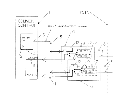
Referring now to Figure 1, the digital switching
system, which might be installed in a small office or home
provided with several ISDN digital circuits, comprises a
common control unit 1 including a phase locked loop system
clock 2 that has an output 3 producing clock signals and
- 3 -
2047641
framing pulses for the system bus, which will be described
in more detail below.
The phase loop 2 has a synchronization input 4 and will
synchronize to clock pulses appearing on the input 4.
The control unit 1 is connected over system bus 5,
which is a 2.048 Mbps ST bus, to basic rate interface cards
6, each comprising a pair of basic rate interface units 7.
The basic rate interface units 7 are connected to respective
basic rate (2B + D) 192 kps circuits 8 connected to the
public network. Each circuit 8 can be in the form of a
standard twisted pair line. Modern echo cancelling
techniques allow such a line to carry digital signals at the
basic rate.
In accordance with the invention, each interface card 6
carries a circuit 9, which in reality is included in the
circuitry of basic rate interface unit 7, for detecting the
synchronization signals on the basic rate circuit 8.
The synchronization signals are are fed through
cascaded switches 10 to clock synchronization lines 11
leading to the synchronization input 4 of the system phase
locked loop 2.
Each interface card 6 is provided with a control
circuit 12 that sets the switches 10 so that only the active
interface unit 7 is connected to the clock synchronization
input 4. The control circuits 12 are controlled by
information nested within an overhead channel on the ST bus.
However, since this information merely designates the active
circuit, only four bits are required to designate a total of
sixteen circuits. Three bits will of course designate eight
circuits and so on.
- 4 -
204?641
Figure 2 illustrates the connection between interface
card 6 and the control unit 1. The card 6 is connected
directly to the phase locked loop 2 over the clock
synchronization line 11 so as to permit the system to be
brought into synchronization with the clock signal on the
basic rate circuits 8. These circuits have a clock
frequency of 1.536 Mhz. The control information is passed
to the cards 7 via the ST bus 5. Each card 6 has includes
dividing logic circuitry (not shown), which lowers the
1.536MHz signal to 8 KHz to further reduce radiation
emissions.
Figure 3 shows the breakdown of a thirty-two channel
frame on the ST bus. The bus has the capability of being
connected to eight circuits, each circuit having four
channel capability. The overhead information determining
the active circuit can be transmitted in the first channel,
since four bits are sufficient to designate up to sixteen
circuits. With the prior art arrangement, each circuit
' required a sixteen bit phase status Word, which therefore
took up substantial bandwidth.
With the described arrangement, there are various other
advantages. The software control of the phase locked loop
can be carried out with low level handling routines,
resulting in improved clock frequency tracking. Also, the
phase locked loop can be implemented in the form of a low
cost analog device.
A further advantage of the described arrangement is
that ponderation (or averaging) of clock source frequencies
can be easily handled by periodically switching between the
clock sources.
- 5 -