Note: Descriptions are shown in the official language in which they were submitted.
2~^7711~ 3 350
SEMICONDUCTOR CONTROL APPARATUS
BACKGROUND OF THE INVENTION
FIELD OF THE INVENTION:
The present invention relates to a semiconductor control
apparatus in which, for example, transistors are used.
DESCRIPTION OF THE RELATED ART:
Fig. 7 is a circuit diagram showing a conventional
semiconductor control apparatus. In the figure, reference
numeral la and lb each denote an insulated gate bipolar
transistor, which is a semiconductor control element,
(hereinafter referred to as an IGBT). Each IGBT has a pair
of main circuit electrodes, that is a collector C and an
emitter E. Each IGBT is further provided with a terminal (e)
on the side of the emitter E which is at a reference
potential, and has a control electrode (g) which is insulated
from the collector C and the emitter E. Reference numeral 2
denotes a bus line on the side of a power supply; reference
numeral 3 denotes a bus line on the side of loads; reference
numeral 4 denotes a first connection conductor on the left
side; reference numeral 5 denotes the inductance of the
connection conductor 4 on the left side shown schematically;
reference numeral 6 denotes a first connection conductor on
the right side; and reference numeral 7 denotes the
~, . .
inductance of the connection conductor 6 on the right side
2~7771
shown schematically. In two IGBTs 1 on the right and left
sides, their collectors C are connected to the power-supply
bus line 2 respectively via second connection conductors 4a
and 6a; their emitters E are connected to the load-side bus
line 3 through the first connection conductors 4 and
respectively.
Reference numeral 10 denotes a control power supply
which is disposed in common with the two IGBTs 1. The
control power supply 10 has two power supplies incorporated
therein: a power supply 11 for closure and a power supply 12
for opening connected as shown in Fig. 7. The negative side
of the power supply 11 for closure and the positive side of
the power supply 12 for opening are connected to a terminal
13. The positive side of the power supply 11 for closure and
the negative side of the power supply 12 for opening are
connected to a terminal 14 via an unillustrated switching
circuit.
Reference numerals lS and 18 each denote a first
connection line, and reference numerals 17 and 20 each denote
a second connection line. The connection lines each connect
the terminals 13 and 14 of the control power supply 10 with
the terminals (e) and control electrodes (g) of the IGBTs 1
on the right and left sides, as shown in Fig. 7. Reference
numeral 16 schematically denotes the inductance of the
connection line 15; reference numeral 19 schematically
~D47~7~
denotes the inductance of the connectlon line 18.
Next, the operation of the conventional semiconductor
control apparatus will be explained. The voltage of the
closure power supply 11 is applied by closlng an
unillustrated switching circuit, so that the terminals (e)
become negative and the control electrodes (g) become
positive. As a result, the sections between the collectors C
and the emitters E conduct in response to the applied
voltage, thereby causing a load current to flow from the
power-supply bus line 2 to the load-side bus line 3. If a
predetermined voltage of the opening power supply 12 is
applied so that the terminals (e) become positive and the
control electrodes (g) become negative, the conductance
between the collector C and the emitter E is blocked, thereby
shutting off a current flowing from the power-supply bus line
2 to the load bus line 3.
Semiconductor control elements generally have variations
in the time (turn-on/turn-off time) from when an
opening/closing signal is given to their control electrodes
to when the section between main circuit electrodes is
opened/closeed. Also, connection conductors and connection
lines for connecting semiconductor control elements or the
like have inductance.
It will now be assumed that the IGBTs la and lb on both
right and left sides become open by a voltage signal from the
2~77~
control power supply 10, whereby a current flowing from the
collector C of each of IGBTs la and lb to the emitter E
thereof is shut off. If the turn-off time of the left IGBT
la should be shorter than the turn-off time of the right IGBT
lb, the current flowing through the IGBT la attenuates
earlier. Therefore, a voltage proportional to the product of
the ratio of change in current which depends on the
characteristics of the IGBT la and the inductance 5 of the
connection conductor 4 on the left side develops across both
ends of the inductance 5, with the voltage having the
polarities shown in Fig. 7, i.e., the load-side bus line 3
becomes positive and the emitter E of the IGBT la becomes
negative. This developed voltage is divided into a plurality
of of voltages having polarities indicated by symbols ~ and
~ in Fig. 7 in proportion to the respective inductances on a
series circuit formed by inductance 7, inductance 19 and
inductance 16. As a result, a voltage smaller than or
greater than the voltage applied from the control power
supply 10 is applied to the control electrode (g) of the
IGBTs la or lb.
Since the conventional semiconductor control apparatus
is constructed as described above, a voltage induced by
inductances 5 and 7 at the time of control, e.g., at
opening/closing time, is applied to inductances 16 and 19
between the control power supply 10 and the terminals (e) of
~0477~1
the IGBTs, with the result that a voltage higher than or
lower than the voltage supplied from the control power supply
10 is applied to the control electrode (g) of the IGBT.
Hence, there occurred cases in which IGBTs malfunctioned or
in some cases IGBTs were destroyed because a voltage above an
allowable voltage for IGBTS was applied thereto.
SUMMARY OF THE INVENTION
The present invention has been devised to solve the
above-mentioned problems. It is accordingly an object of the
present invention to obtain a highly reliable semiconductor
control apparatus which is capable of stably controlling a
plurality of semiconductor control elements, one of the main
circuit electrodes being connected in common, by means of a
common control power supply.
In the semiconductor control apparatus of the present
invention, a transformer having a first coil and a second
coil which is made to have the same polarity as that of the
first coil is disposed. The first coil is inserted between
the control power supply and one of the main circuit
electrodes of a semiconductor control element. The second
coil is inserted between the control power supply and the
control electrode of the semiconductor control element.
In the transformer of the present invention, a first
coil is made to have a voltage generated on one of the main
circuit electrodes of a semiconductor control element when
2~'1771
the semiconductor control element is controlled. A voltage
having the same polarity as that of the above voltage is
generated, by a second coil, between the control power supply
and the control electrode of IGBT. Thus, the voltage
generated on the one side of the main circuit electrodes is
cancelled or offset, thereby causing no abnormal voltage to
be applied to the control electrode.
BRIEF DESCRIPTION OF THE DRAWINGS
Fig. 1 is a circuit diagram showing an embodiment of a
semiconductor control apparatus of the present invention;
Fig. 2 is a circuit diagram showing another embodiment
of the semiconductor control apparatus of the present
nventlon;
Figs. 3 through 6 are views showing other elements used
as semiconductor control elements in the present invention;
and
Fig. 7 is a circuit diagram showing this type of a
conventional semiconductor control apparatus.
DESCRIPTION OF THE PREFERRED EMBODIMENTS
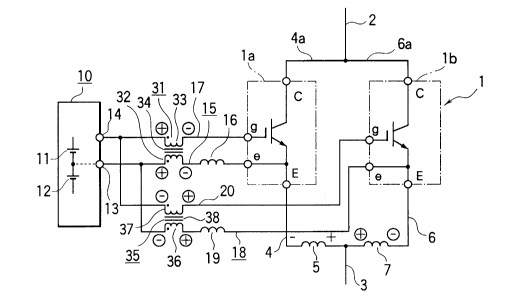
Fig. 1 is a circuit diagram showing an embodiment of a
semiconductor control apparatus of the present invention.
Transformers 31 and 35 are disposed between a control power
supply 10 and, respectively IGBTs la and lb. The transformer
31 comprises a first coil 32 and a second coil 33, both of
. ~
which are wound around an iron core 34 the same number of
-- 6
20~7~71
turns to the same polarity, as shown in Fig. 1. The first
coil 32 is inserted into a first connection line 15 for
connecting a terminal 13 of the control power source 10 with
a termlnal (e) of the IGBT la. The second coil 33 ls
inserted into a second connection line 17 for connecting z
terminal 14 of the control power supply 10 with the control
electrode (g) of the IGBT la. The construction of the
transformer 35 is the same as that of the transformer 31. A
first coil 36 and a second coil 37 are wound around an iron
core 38 the same number of turns to the same polarity. These
coils are connected to the polarity shown in Fig. 1 between
the control power supply 10 and the right IGBT lb. Since the
other components in Fig. 1 are the same as those of the prior
art shown in Fig. 7, the same reference numerals are given to
corresponding components, and an explanation thereof is
omitted.
Next, an explanation will be provided of the operation
of the semiconductor control apparatus. It will be assumed
now that the state of both IGBTs la and lb is changed from a
conducting state to a non-conducting state by a signal from
the control power supply 10 in the same manner as in the
prior art in Fig. 7, thereby the main circuit electrodes of
the IGBTs la and lb shut off a current flowing from the
collector C to the emitter E. For example, if the turn-off
time of the IGBT la is shorter than the turn-off time of the
204~
IGBT lb, the current flowing through the IGBT la attenuates
earlier. Regarding a voltage induced in the inductance 5, as
shown in Fig. 1, the side of the IGBT la has a negative
polarity and the side of the load-side bus line 3 has a
positive polarity ln the same manner as in the prior art.
This developed voltage is divided by the ratio of impedance
of an inductance 7, an inductance 19, the first coil 36 of
the transformer 35, the first coil 32 of the transformer 31,
and the inductance 16, on a series circuit including a first
connection conductor 6 on the right side thereof, first
connection lines 18 and 15, and transformers 35 and 31.
Exciting impedance values of the transformers 31 and 35
sufficiently larger than the impedance of inductances 16 and
19 are selected, with the result that the first coil 32 of
the transformer 31 and the first coil 36 of the transformer
35 are burdened with most of the voltage induced in the
inductance 5. The same voltage which has the same polarity
as the voltage applied to these first coils 32 and 36 is
induced in the second coils 33 and 37 respectively. As a
result, the respective voltage amounts applied to the
sections between the emitters E and the control electrodes g
of the IGBTs la and lb are cancelled each other by the first
coil 32 and the second coil 33 of the transformer 31, and the
first coil 36 and the second coil 37 of the transformer 35
respectively. Since the respective impedance amounts of the
2 ~
transformers 31 and 35 seen from the control power supply 10
become zero, this fact causing no hindrance to a signal
applied to the section between the control electrode (g) and
the terminal ~e) of each of the IGBTS la and lb. A desired
signal can be supplied to the section between the control
electrode (g) and the terminal (e).
Fig. 2 shows another embodiment of the present
invention. The power supply sides of the IGBTs la and lb,
i.e., the side of the collectors C, are respectively
connected to bus lines 41 and 42 which are connected to
individual power supply portions. IGBTS la and lb are
controlled at different timings by the control power supply
10. In this case, terminals 43 and 44 are disposed in the
control power supply 10 in addition to terminals 13 and 14
and the power supply 11 for closure and the power supply 12
for opening are connected as shown, so that right and left
IGBTS la and lb can be individually controlled by the control
power supply 10. The voltage of the power supply 11 for
closure or that of the power supply 12 for opening is
individually applied between the control electrodes (g) and
the terminals (e) of the IGBTS la and lb by closing a
switching circuit (not shown). Capacitors 45 and 46 are
capacitors for absorbing surge, and are disposed respectively
between the control electrode (g) and the terminal (e) of
each of the IGBTS la and lb, that is each capacitor is
204~ 771
connected between the first and second connection lines.
In the semiconductor control apparatus shown in Fig. 2
and constructed as described above, the IGBTS la and lb are
controlled independently of each other. A voltage developed
across the inductance 5 or the inductance 7 when each of the
IGBTs la and lb are opened/closed is compensated respectively
by transformers 31 and 35. Hence, the voltage does not
develop between the control electrode (g) and the terminal
(e) in the same manner as in the embodiment of Fig. 1.
In each of the embodiments described above, a case was
shown where transformers 31 and 35 are singly inserted
between the control power supply 10 and the control electrode
(g) of each of the IGBTs la and lb respectively. However,
the same effect can be achieved if other impedance elements
are inserted in series in addition to the transformers 31 and
35. The ratio of number of turns of the first and second
coils of the transformers 31 and 35 need not necessarily be 1
to 1.
Although a case where semiconductor control elements are
IGBTS was shown in each of the embodiments described above,
needless to say, the same effect can be obtained (a) if
voltage driven type semiconductor control elements which are
the same as IGBTS, such as insulated gate bipolar transistors
which are like MOSFETs, as shown in Fig. 3, are used, (b) if
~,
current driven type semiconductor control elements, such as
-- 10 --
~04 777 1
bipolar transistors shown in Fig. 4, are used, and (c) if
semiconductor control elements, such as thyristors or gate
turn-off thyristors (GTO) shown in Figs. 5 and 6, are used.
As has been explained above, according to the present
invention, a transformer is disposed between each
semiconductor control element and a control power supply
respectively so as to cancel a voltage developed at the time
the semiconductor control elements are controlled, thereby
causing no abnormal voltage to be applied to the control
electrodes of the semiconductor control elements. Therefore,
a highly reliable semiconductor control apparatus in wnich
semiconductor control elements do not malfunction and no
insulation breakdown occurs can be obtained.
. .