Note: Descriptions are shown in the official language in which they were submitted.
20478q~
BEAM SCAN VELOCITY MODULATION
APPARATUS W~TH DISABLING CIRCUIT
This invention relates to beam scan velocity modulation (SVM)
5 systems employed for picture sharpness enhancement.
It is well known that an improvement in apparent picture
resolution can be achieved by the use of modulation of the beam scan
velocity in accordance with the derivative of the video signal which
controls the beam intensity. This video signal is known as the
10 luminance signal and the derivative of the luminance signal is
employed for beam scan velocity modulation (SVM). Beam scan
velocity modulation will improve the picture sharpness in a color
television system employing a color kinescope.
Many modern color television receivers also employ alternate
15 video sources. An example of such an alternate video source is
commonly referred to as an On Screen Display (OSD) generator. The
function of the OSD generator is to provide additional display
i nformation to a viewer while viewing a typical television program.
Thus OSD generators provides for the display on the television screen
~0 of the time of day, channel number, and various control information.
In implementing OSD display, the OSD information is presented
together with the normal picture. For example, as illustrated in
FIGURE 2, the television screen may display the word "MUTE", which
word display is generated by the OSD generator. This indicates to the
2 5 user that the sound associated with the television picture is turned
off.
Techniques for generating this type of graphical data which is
superimposed upon the television picture are well known. Such
techniques include OSD generators which count television lines and
3 0 insert at the correct pixel locations the proper graphics to display the
time of day, the channel number, words such as "CONTRAST", "COLOR",
"MUTE", and so on. The use of an on screen display and an associated
OSD generator requires the substitution of a different video signal or
kinescope drive for the normal video signal which is being processed
3 5 by the television receiver. In this manner the pertinent information
can be superimposed upon the viewed image.
A problem may occur in regard to scan velocity modulation in
television receivers which also include an alternate video source such
as on screen display generator. As is known, the SVM apparatus
~0~7~98
- 2 - RCA 85,813
. . .
operates to modulate the horizontal beam scan velocity in response to
differentiated luminance information from the main video source.
This modulation may occur prior to OSD deletion of the main
luminance signal and insertion of the character signal. In this
5 arrangement, the OSD signal path to the kinescope or display device
may bypass the SVM apparatus. As a result, a ghost image
representative of the deleted portions of the main luminance signal
may appear on the television screen near or behind the inserted OSD
character information. Since the horizontal scan is being modulated
10 by the SVM coil in accordance with the differentiated luminance
signal, e,g. in accordance with lumin~nce edges, the ghost image
behind the characters generated by the OSD display appears as an
outline of the picture contained in the deleted portions of the main
luminance signal.
It is therefore desirable to eliminate the above-noted
interference and to substantially decrease the effect of SVM artifact
generation during the operation of an OSD generator in a television
receiver.
A scan modulating circuit modulates the picture displayed on a
2 0 display device in accordance with the video content of a first video
signal. An alternate video signal has its picture information displayed
on the display device when the alternate video signal is selected.
Operation of the scan modulation circuit is, however, modified in
accordance with this selection.
FIGURE 1 is a block diagram circuit of a color television receiver
employing beam scan velocity modulation according to the invention.
FIGURE 2 is a diagrammatic view depicting a video display
useful in explaining the operation of the circuit of FIGURE 1.
FIGURE 3 is a detailed circuit diagram of the beam scan velocity
3 0 modulation and disabling apparatus of FIGURE 1 embodying the
invention .
FIGURES 4a and 4b are waveforms useful in explaining the
operation of the circuitry depicted in FIGURE 3.
In the color television receiver 10 of FIGURE 1, an antenna 11 is
3 5 conventionally coupled to a tuner 12. The output of tuner 12 is
applied to an IF stage 13. The output of IF stage 13 is directed to the
input of a comb filter 14. Filter 14 provides one output which is
directed to the input of a luminance processor 15 for processing the
luminance signal and another output which is directed to a chroma
3 ~4~898 RCA 85~8l3
demodulator 16. Luminance processor 15 is a conventional circuit
and responds to the luminance signal contained in the composite color
video signal developed at the output of IF stage 13. Chroma
demodulator 16 provides the color difference signals such as the R-Y
and the B-Y signals.
The luminance signal Y from the output of luminance processor
15 and the color difference signals from the output of chroma
demodulator 16 are applied to a stage 17. Stage 17 is designated as
an RGB matrix and OSD insertion stage. Stage 17 receives the color
l O difference signals, and the luminance signal and, in one mode,
operates strictly as an RGB matrix. In this mode, the matrix
conventionally processes the color difference signals with the
luminance signal to provide the red (R), green (G), and blue (B)
signals. The R, G, B, signals are applied to a kinescope driver circuit
20, which circuit drives a color kinescope 21 associated with a
conventional color television.
Located on the neck of kinescope 21 is a main deflection yoke
23 comprising respective horizontal and vertical deflection windings,
each of which are subjected to energization by respective horizontal
2 0 and vertical deflection circuits (not illustrated) to develop a raster of
scanning lines on the viewing screen of the kinescope 21.
Supplemental deflection of the respective beams in the kinescope is
supplied by an auxiliary deflection coil 26 which operates to provide
scan velocity modulation. SVM Coil 26 may be a single coil or a coil
having multiple windings. In any event, one can provide scan
velocity modulation by other means such as by deflector plates using
electrostatic deflection instead of magnetic deflection. Energization of
SVM coil 26 is provided by a scan velocity modulation stage 35, to be
further described.
A luminance video signal YS is generated by luminance
processor 15 and is indicative of the wideband luminance signal Y
that is applied to matrix stage 17. Luminance video signal YS is
applied to an input buffer amplifier 30 of SVM stage 35. The output
of amplifier 30 is coupled to the input of a differentiator circuit 31,
3 5 whereby the amplified video signal is differentiated. The
differentiated video signal is then applied to the input of a limiter or
limiting amplifier 32. The limiter operates to limit excursions of the
differentiated video signal in both the positive and negative
directions in regard to normal operation. The output of limiting
2n4789~
-4- RCA 85,813
amplifier 32 is applied to the input of a driver amplifier 33 which
serves to further process the signal, e.g. to provide noise coring. The
output of driver amplifier 33 is coupled to the input of an output
power amplifier 34 for converting the input voltage to the power
amplifier into an output current. This current is proportional to the
magnitude of the differentiated video signal and is used to drive SVM
coil 26.
SVM stage 35 has a signal delay characteristic matched to that
of the luminance signal being processed by stages 15, 17 and 20. In
this way, correctly timed edge enhancement of the displayed picture
can be obtained.
As previously indicated, many modern television receivers are
capable of OSD operation. In regard to OSD operation, such receivers
include an OSD generator 40. The OSD generator may include a
horizontal line counter and be responsive to the vertical sync signal to
enable text or graphics to be selectively superimposed upon the
image displayed on the kinescope screen. To superimpose the OSD
information, an output of OSD generator 40 is coupled via a signal line
40b to RGB matrix and OSD insertion stage 17. Switching signals on
2 0 this line enable RGB matrix stage 17 to delete the original picture
information drive signals and substitute OSD character drive signals.
SVM stage 35 operates in conjunction with the differentiated
luminance signal from the main signal source and thus operates even
though the signal being applied to kinescope 21 is partly derived
from an alternate signal source such as OSD generator 40. During
operation of the OSD generator, the OSD signal path to the kinescope
or display device bypasses the SVM circuitry. This may result in the
previously described visually undesirable artifacts appearing on the
television screen.
In order to further understand the nature of the interaction
between OSD generation and SVM operation, reference is made to
FIGURE 2, which depicts a typical television scene 36, whereby an OSD
generator operates to produce the word "MUTE". The word "MUTE"
appears on the screen in any type of graphic format as depicted by
3 5 reference number 38. It is noted that the word "MUTE" is generated
by the OSD generator during a given number of selected horizontal
lines 37 and therefore can be of any size or shape and at any location
on the screen. Ghost images of scene 36 could appear behind or ne;lr
the display of the word "MUTE", since SVM stage 35 responds to the
~0~7~98 RCA 85,813
-
deleted luminance information rather than to the generated character
information.
To eliminate this effect, in accordance with an aspect of the
invention, SV~ stage 35 is selectively disabled from normal operation
5 during OSD character generation or during picture display intervals
associated with an alternate video source. As shown in FIGURE 1, an
output signal line 40c from OSD generator 40 is coupled to SVM stage
35 to alter SVM operation during OSD generation and substantially
reduce the appearance of visual artifacts during OSD operation.
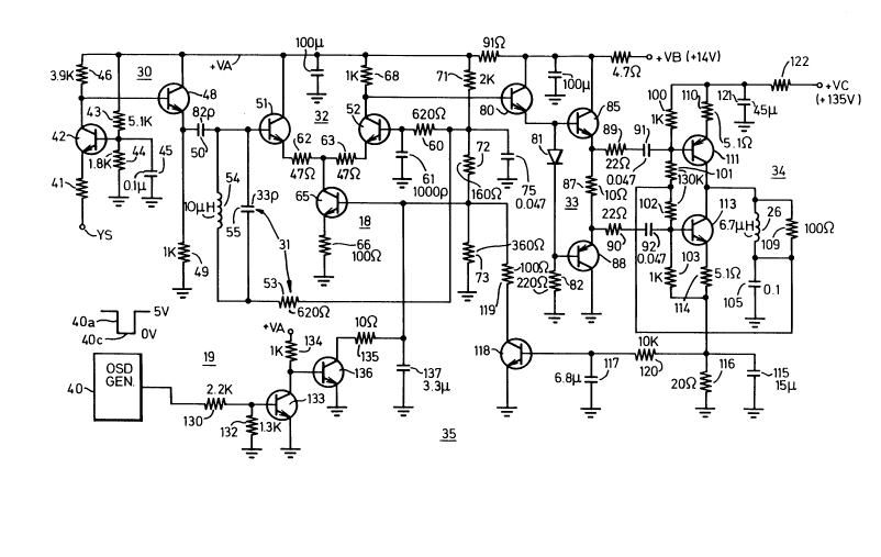
l 0 FIGURE 3 illustrates a portion of the circuitry of FIGURE 1,
including a detailed embodiment of SVM stage 35. In FIGURE 3,
luminance video signal YS is applied via a resistor 41 to the emitter
electrode of a transistor 42 arranged in a common base configuration.
Base biasing for the common base transistor is obtained by a voltage
l 5 divider comprising resistors 43 and 44 coupled between a source of
operating potential +VA and ground. A bypass capacitor 45 is
coupled between ground and the base electrode of transistor 42. The
collector electrode of transistor 42 is directed through a load resistor
46 to the source of operating potential +VA. The collector electrode of
2 0 transistor 42 is also coupled to the base electrode of a transistor 48
arranged in an emitter follower configuration. The collector electrode
of transistor 48 is coupled to the source of operating potential +VA,
and the emitter electrode is directed to ground via a resistor 49. The
emitter electrode is also AC coupled via a capacitor 50 to the base
2 5 electrode of a transistor 51. Transistor 51 is part of the differential
limiting amplifier 32 of FIGURE 1.
The base of transistor 51 is coupled to a tank circuit comprising
an inductor 54 in shunt with a capacitor 55. The tank circuit operates
to provide a flattened group delay in regard to operation of
3 0 differentiator 31 so as to compensate for the characteristic of the
differentiator, thereby linearizing the differentiated output with
regard to high frequency operation. Differentiator 31 comprises
capacitor 55 and a resistor 53. Resistor 53 has one terminal coupled
to a terminal of the tank circuit remote form the base of transistor 51
3 5 and another terminal coupled to the junction between resistors 71
and 72 of a voltage divider comprising resistors 71, 72 and 73. The
voltage divider establishes the bias point of the differential limiting
amplifier .
- 6 ~ 8 ~ ~ RCA 85,813
Differential limiting amplifier 32, includes transistor 51 and a
transistor 52. Transistor 51 has a collector electrode directly coupled
to the source of operating potential +VA and an emitter electrode
coupled via a resistor 62 to a controllable current source 18, at the
collector electrode of a transistor 65. Transistor 65 has the emitter
electrode coupled through a resistor 66 to ground. In a similar
manner transistor 52, has its emitter electrode coupled to the
collector electrode of constant current source transistor 65 via a
resistor 63. Resistors 62 and 63 may be equal in magnitude. The
1 0 collector electrode of transistor 52 is coupled to the source of
operating potential +VA via a collector load resistor 68. The collector
electrode of transistor 52 provides the output of limiting amplifier 32.
The base electrode of transistor 52 is coupled to the junction between
resistors 71 and 72 via a resistor 60. The base electrode of transistor
1 5 52 is coupled to ground by a capacitor 61 which operates as a bypass
for high frequency signal components. DC biasing for transistor 51 is
obtained via the connection of resistor 53. Resistor 60 and resistor 53
are of the same magnitude to enable transistors 51 and 52 to receive
equal DC biasing. The base electrode of current source transistor 65 i s
2 0 coupled to the junction between voltage dividing resistors 72 and 73
and is also coupled to the collector electrode of a control transistor
118, for controlling the current through limiting amplifier 32. This
control varies the peak-to-peak output signal of the limiter, as will be
further explained, and also provides double ended limiting.
The collector electrode of transistor 52 is directly coupled to the
base electrode of an emitter follower transistor 80. The collector
electrode of transistor 80 is coupled to a source of operation potential
+VB, and the output emitter electrode is coupled to a driver stage 33.
Driver stage 33 comprises complementary type transistors 85
3 0 and 88, with the base of transistor 85 being directly coupled to the
emitter of transistor 80 and with the base of transistor 88 being
coupled to the emitter of transistor 80 via a diode 81. Diode 81 is
directly coupled between the bases of the two driver transistors. A
resistor 87 is coupled between the emitters of transistors 85 and 88,
3 5 and a resistor 82 is coupled between the base of transistor 88 and
ground. Transistors 85 and 88 form a Class B amplifier which
operates to drive output stage 34. The Class B amplifier also provides
a low level, noise coring function.
2 0 ~ 9 8
- 7 - RCA 85,813
The emitter electrodes of transistors 85 and 88 in Class B driver
stage 33 are AC coupled to the respective base electrodes of
complementary type transistors 111 and 113 of output stage 34. To
provide the AC coupling, the emitter electrodes of transistors 85 and
88 are coupled through respective resistors 89 and 90 in series with
respective capacitors 91 and 92.
The emitter electrode of transistor 111 is directed through a
resistor 110 to a source of operating potential +VC. A resistor 122
and a capacitor 121 provide current limiting and supply filtering.
I 0 The source of operating potential +VC is a DC source of relatively high
magnitude, as for example, 135 volts, compared to the source of
potential +VB, as for example,14 volts. This enables output amplifier
stage 34 to supply high frequency current to SVM coil 26.
The collector electrode of transistor 111 is coupled to the
1 5 collector electrode of transistor 113, thereby forming a Class B output
stage. Biasing for the output stage transistors is obtained from a
voltage divider comprising resistors 100, 101, 102, and 103. The
emitter electrode of transistor 113 is coupled to ground via a resistor
114 and a current sampling resistor 116. Resistor 116 is shunted by
means of a filter capacitor 115. The time constant for the RC filter of
resistor 116 and capacitor 105 is on the order of 20 to 30 horizontal
line periods.
One terminal of SVM coil 26 is directed to the junction of the
collector electrodes of transistors 111 and 113, and the other terminal
is coupled to a grounded capacitor 105. In this manner, the SVM coil
is AC coupled to output stage 34, and no DC current can flow in the
coil. A damping resistor 109 is coupled across the SVM coil. DC
stabilization is provided by coupling the junction of SVM coil 26 and
capacitor 105 to the junction of resistors 101 and 102.
3 0 Output stage 34 includes current feedback afforded by resistor
116 to prevent overdissipation in the output stage when luminance
signal YS has, on the average, substantial high frequency content. The
average current through output stage 34 flows through sampling
resistor 116. The filtered voltage developed across resistor 116 is
3 5 representative of this output current and is coupled to the base
electrode of a transistor 118 via a resistor 120. The base electrode of
transistor 118 is bypassed to ground through a capacitor 117. The
magnitude of capacitor 117 is selected to greatly attenuate any high
frequency signals and noise that may be undesirably coupled to
-8~ 7~ RCA 85,813
transistor 118. The collector electrode of transistor 118 is coupled via
a resistor 119 to the junction between voltage dividing resistors 72
and 73, at the base electrode of constant current transistor 65.
An increase in current through output stage 34 due to, for
5 example, an increase in average high frequency content of video
signal YS, results in an increase in conduction of transistor 118 and
therefore a decrease in current in transistor 65. The decrease in
current in transistor 65 results in a decrease in peak-to-peak output
response. The result is a decrease in average drive to output stage 34,
1 0 thereby preventing over dissipation in the output stage.
OSD generator 40 of FIGURES 1 and 3 provides OSD blanking
pulses 40a, on a line-by-line basis, to matrix stage 17 during the
interval of OSD character generation. These blanking pulses are also
coupled to an SVM disabling circuit 19 for selectively disable normal
1 5 SVM operation during OSD generation.
In FIGURE 3, a negative going OSD blanking pulse 40a is applied
via a resistor 130 to the base electrode of a transistor 133. A resistor
132 is coupled between ground and the base electrode of transistor
133. The collector electrode of transistor 133 is coupled to the base
20 of an SVM disabling transistor 136. DC base biasing for transistor 136
is obtained from the +VA operating potential via a resistor 134. The
collector electrode of transistor 136 is coupled via a resistor 135 to
the base electrode of constant current source transistor 65. The base
electrode of constant current source transistor 65 is also coupled to
2 5 ground via a capacitor 137 which, as will be explained, is relatively
large in value.
When OSD generator 40 is operative to produce character
generation for a given block of horizontal lines, the OSD generator will
generate a series of blanking pulses 40a within each line period of the
30 block of lines. These pulses correspond to the OSD insertion points for
each line. Any given one of blanking pulses 40a will switch on
transistor 136 for the duration of that pulse, rapidly discharging
capacitor 137, and diverting base current from transistor 65. The
current source for differential amplifier 32 is thereby turned off or
3 5 substantially reduced in magnitude, depending on the value of
resistor 135 in series with the collector of transistor 136. For
example,the magnitude of current source 18 may be reduced to the
point that the peak to peak output of differential amplifier 32 is
9 ~ ~ RCA 85,813
reduced by 20 db from normal levels. Under certain circumstances,
even a reduction of as little as 6db may have beneficial effects.
As a result of the operation of disabling circuit 19, no significant
amounts of differentiated video signal is supplied to output stage 34.
SVM coil 26 does not become significantly energized during OSD
operation, thereby preventing visually disturbing artifacts from
appearing on the television screen.
After completion of OSD generation, blanking pulses 40a are no
longer being generated, resulting in disabling transistor 136 being
1 0 turned off. In accordance with a different inventive feature, current
source transistor 65 does not immediately become conductive when
transistor 136 is turned off. Instead transistor 65 remains in cutoff
or near cutoff for an interval that depends upon the time it takes
discharged capacitor 137 to recharge to a level that will forward bias
l 5 the base-emitter junction of the transistor to normal bias values. The
recharging time is a function of the RC time constant associated with
capacitor 137 and voltage dividing resistors 71, 72 and 73, as well as
the value of operating potential +VA and the base current circuit
parameters of transistor 65. By selecting capacitor 137 to be
2 0 relatively large, a delay equivalent to e.g. 20 or 30 horizontal lines is
provided. This results in a relatively slow resumption of normal SVM
operation after termination of OSD generation.
The relatively slow resumption of normal SVM operation is
advantageous in several respects. For example, when disabling circuit
19 is connected to SVM stage 35 in the manner shown in FIGURE 2,
differential amplifier 32 becomes disabled when current source
transistor 65 becomes disabled. The collector electrode of transistor
52 is then pulled up to the +VA voltage level. This level is then
translated by the successive base-emitter junctions in transistors 80
and 85, and coupled to DC blocking capacitors 91 and 92, altering
their charge levels. -
Assume current source transistor 65 were to resume full
conduction immediately upon termination of OSD generation. Then
operation of differential amplifier 32 would also resume immediately.
3 5 Full peak-to-peak amplitude SVM drive would be immediately
restored to output amplifier stage 34. However, because of the
altered charge levels in capacitors 91 and 92, the wrong DC drive
level would be applied to the output amplifier, causing erroneous and
undesirable scan velocity modulation of the electron beams. This
2 ~ ~ '6~
-10 - RCA 85 ,8 1 3
undesirable modulation is at full AC drive, and would continue until
correct charge levels are established in DC blocking capacitors 91 and
92.
It may be possible to avoid the above described undesirable DC
5 transients by the expedient of decreasing the values of capacitors 91
and 92 by, e.g., a factor of 10 or more. This, however, could introduce
an undesirable alteration of SVM pulse waveshape due to a resultant
inequality in the propagation time of the different component
frequencies that constitute the SVM pulse.
By providing capacitor 1 37 , coupled to the base electrode of
current source transistor 65, conduction in the transistor slowly
increases upon termination of OSD generation. The peak-to-peak
SVM drive waveform at the collector electrode transistor 52 slowly
increases to normal, full amplitude in a way that tracks the
15 reestablishment of correct charge levels in DC blocking capacitors 9 1
and 92. This slow turn on of differential amplifier 32 avoids the SVM
overdriving conditions that could otherwise occur upon termination of
OSD display.
Referring to FIGURE 4, FIGURE 4a depicts on a vertical interval
2 0 time scale, the envelope waveform of SVM current which flows
through coil 26 of FIGURES 1 and 3. FIGURE 4b, on the same time
scale, depicts the inverted cathode voltage which is applied to any
representative one of the kinescope cathodes. The closely spaced
vertically oriented lines in the waveforms of FIGURES 4a and 4b
2 5 schematically represent the higher frequency content of the signals.
In FIGURE 4b the term "MUTE" identifies the interval in a given
vertical field when the word "MUTE" appears on the television screen.
As one can see, the SVM current of FIGURE 4a during this interval, is
reduced to zero. This reduction is implemented relatively fast (FAST
30 OFF). SVM current returns to normal levels relatively slowly (SLOW
ON), after completio~ of character generation. Capacitor 137, as
indicated previously, provides for the slow recovery time, equivalent
to, e.g., 20 or 30 horizontal lines.