Note: Descriptions are shown in the official language in which they were submitted.
JA9-90-005 2047905
LIQUID ~KYsl-AL DISPLAY
The invention relates to an active matrix type liquid
crystal display using a thin film transistor (thereafter
referred to as TFT) as switching element, and is
particularly concerned with the liquid crystal display which
allows a flicker on a screen to be reduced.
The invention will be more readily understood from the
following disclosure taken in conjunction with the appended
drawings wherein:
FIG.l is a diagram showing the construction of a liquid
crystal panel according to an embodiment of the invention.
FIG.2 is a diagram showing the construction of a liquid
crystal panel according to other embodiment of the
lnventlon .
FIG.3 is a diagram showing the construction of the
conventional liquid crystal panel.
In a conventional liquid crystal display using an active
matrix typed liquid crystal panel, AC drive is applied to
liquid crystal elements by inverting the polarity of data
signals to be applied to prevent the liquid crystal elements
from worsening their property. FIG.3 is a schematic diagram
showing a construction of a conventional liquid crystal
display as described above. In the figure, a gate driver 1
is connected to n row conductors Gl to Gn to which scanning
signals are sequentially outputted. A first data driver 2
is connected to odd column conductors Dl to Dm-l to which
first data signals are outputted. On the other hand, a
second data driver 3 is connected to even column conductors
D2 to Dm to which second data signals are outputted. TFTs
4a, 4b, 4c, and 4d are provided at the respective
intersections of the row conductors and the column
conductors, each one of their gate electrodes being
connected to corresponding one of row conductors, each one
JA9-90-005 2347~0~
of their drain electrodes being connected to corresponding
one of data signal lines, their respective source electrodes
being connected to subpixels 5a, 5b, 5c, and 5d described
later. The subpixels 5a, 5b, 5c, and 5d each of which is
formed by a crystal cell, are driven by the above TFTs 4a,
4b, 4c, and 4d, respectively.
For an areal gradation of these subpixels, a single pixel is
comprised of these four adjacent subpixels 5a, 5b, 5c, and
5d vertically or horizontally arranged. In this case, a
predetermined level of gradation can be displayed by
selecting properly the ratio of the sizes of the subpixels
5a, 5b, 5c, and 5d.
In the following, a conventional method for driving
subpixels is described using FIG.3.
First, when gate signals are sequentially applied to each
gate electrode of the TFTs 4a, 4b, 4c, and 4d, connected to
the row conductors, from the gate driver 1 in response to
control signals from a controller (not shown), TFTs 4a, 4b,
4c, and 4d are sequentially turned on state. A first and a
second data signals are applied to each column conductor
simultaneously with the above gate signals, from the first
data driver 2 and the second data driver 3. The first and
the second data signals have the same or opposite polarity
inverted every frame.
When the first and the second data signals are signals of
the same polarity, subpixels on the entire display screen
are inverted and driven by alternating current every frame.
On the other hand, when the first and the second data
signals are signals of the opposite polarity, subpixels on
the entire display screen are inverted and driven by
alternating current every subpixel in row direction.
In the conventional liquid crystal display as described
above, when data signals with the same phase each other,
JA9-90-005 3
204793~
inverted every frame are applied to each odd data signal
line and each even data signal line respectively, noticeable
flicker on the screen comes into question since the entire
display screen is driven by alternating current inverted
every frame.
It will be appreciated also that when data signals with the
inverse phase each other, inverted every frame are applied
to each odd data signal line and each even data signal line
respectively, noticeable flicker on the screen comes into
question almost the same as the case where data signals with
the same phase each other are applied as described above
since the entire display screen is driven by alternating
current inverted every subpixel in the row direction and is
not driven invertedly every pixel in an attempt to
invertedly drive every data signal line in the case of an
areal gradation of the four adjacent subpixels, arranged
vertically and horizontally, formed into one pixel.
An object of this invention is to solve the above problems
and to provide a liquid crystal display on which 16 levels
of gray scales can be displayed so as not to take notice of
flicker on a display screen.
A liquid crystal display concerned with the invention
including a plurality of row conductors, a plurality of
column conductors, a plurality of subpixels arranged like
matrix, and means for alternately applying a first and a
second data signals to said column conductors every two
column conductors, said subpixels in the same row being
connected to the same row conductor, one column of adjacent
subpixels of each pixel in the column direction being
alternately connected, every two row conductors, to a
conductor to which said first data signal is supplied and to
a conductor to which said second data signal is supplied,
the other column of adjacent subpixels of said each pixel in
the column directi.on being alternately connected, every two
column conductors, to said conductor to which said first
data signal is supplied and to said conductor to which said
JA9-90-005 4
2047qO5
second data signal is supplied. It will be appreciated also
that a liquid crystal display concerned with the inventions
including a plurality of row conductors, a plurality of
column conductors, a plurality of subpixels arranged in a
matrix, and means for applying alternately a first and a
second data signals to said column conductors every two
column conductors, said subpixels in the same row being
connected to the same row conductor, the polarity of said
first and said second data signals being alternately
inverted every two row conductors.
According to this invention, a first data signal of one
polarity and a second data signal of the opposite polarity
are applied and the polarity of said first and second data
signals is inverted at a repetition interval which is
substantially the same as a frame interval.
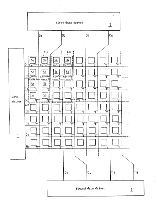
FIG.l is a construction example showing an embodiment of a
8x8 matrix type liquid crystal panel of a liquid crystal
display according to the invention. In the figure, a gate
driver 1 is connected to row conductors Gl to G8 and
sequentially outputs scanning signals to the row conductors
Gl to G8. Column conductors Dl to D8 are alternately
connected to a first data driver 2 and a second data driver
3 every column conductor. The first data driver 2 and the
second data driver 3 output the first data signal of one
polarity and the second data signal of the opposite
polarity, respectively. The gate electrodes of TFTs 4a and
4b and TFTs 4c and 4d are connected to row conductors Gl,
3 5 7 2' G4, G6, and G8, respectively On the
other hand, the respective source electrodes of the TFT 4a,
TFT 4b, TFT 4c, and TFT 4d are connected to subpixels 5a,
5b, 5c, and 5d. Moreover, the drain electrodes of the TFTs
4a, 4b, 4c, and 4d are alternately connected to the first
group of the column conductors Dl and D2, and D5 and D6
connected to the first data driver2 and the second group of
the column conductors D3 and D4, and D7 and D8 connected to
the second data driver 3 every two column conductors. Each
P 611' 612 - 621, 622 - - is comprised of four
JA9-90-005 5
2047905
adjacent subpixels 5a, 5b, 5c, and 5d. In the figure, the
subpixels 5a, 5b, 5c, and 5d are illustrated, for
convenience, so that their area ratio is not different.
However, as in the embodiment, if an attempt to perform 16
levels of display is made by an areal gradation of one pixel
based on combinations of ON/OFF for the subpixels 5a, 5b,
5c, and 5d whose area ratio is different, the subpixels 5a,
5b, 5c, and 5d may be defined so that the ratio of their
respective areas A, B, C, and D is 8:2:4:1.
Now, the preferred embodiment of the invention is described
by reference to the figure.
When a control signal is sent out to the gate driver 1, the
first data driver 2, and the second data driver 3 from a
control unit not shown in the figure, the gate driver 1, the
first data driver 2, and the second data driver 3 are driven
respectively. When the gate driver 1 is driven, scanning
signals are sequentially applied to the row conductors G1 to
G8. When the scanning signals are applied, the TFTs 4a, 4b,
4c, and 4d of respective pixels 6 are sequentially turned
on. A first data signal of one polarity from the first data
driver 2 and a second data signal the polarity of which is
opposite to that of the first data signal, from the second
data driver 3 are applied, simultaneously with the scanning
signals, to the first group of the column conductors Dl and
D2, and D5 and D6 and the second group of the column
conductors D3 and D4, and D7 and D8, respectively. In this
case, the scanning signals from the gate driver 1 cause the
switches (not shown) of the first data driver 2 and the
second data driver 3 to switch, every two row conductors,
that is, every each of G1 to G2, G3 to G4, and G6 to G8, and
first data signals and second data signals applied to the
column conductors D1 to D8 to be inverted. Thus, adjacent
pixels, pixels 611 and 612, pixels 621 and 622, pixels 6
and 621, and pixels 612 and 622 are invertedly driven.
Likewise, other adjacent pixels are thus invertedly driven
to remove flicker on a display screen. Since a liquid
crystal panel is driven by alternating current, the polarity
JA9-90-005 6 2 0 4 7 9 0 5 ~
of a first data signal and that of a second data signal
described above, are inverted every frame and that of the
first and the second data signals are invertedly driven
every adjacent pixel and thus flicker can be removed from
the display screen, as described above.
FIG.2 is a construction example showing another embodiment
of a 8x8 matrix type liquid crystal panel of a li~uid
crystal display according to the invention. FIG.2 is the
same as FIG.l except that the connection of subpixels is
different from each other. Referring to FIG.2 to describe
the connection of subpixels, adjacent subpixels 5a and 5b,
and 5c and 5d of pixels 6 in the row direction are
alternately connected to column conductors connected to a
first data driver 2 and column conductors connected to a
second data driver 3. Also, adjacent subpixels 5a and 5c,
and 5b and 5d of the pixels 6 in the column direction are
alternately connected to the column conductors connected to
the first data driver 2 and the column conductors connected
to the second data driver 3, respectively, every two row
conductors. For convenience of the description, for example
pixels 612 is shown as an example of the connection of
subpixels in the following. In the example, the gate
electrodes of TFTs 4a and 4b and TFTs 4c and 4d are
connected to the row conductor Gl and the row conductor G2,
respectively. On the other hand, the drain electrodes of
the TFTs 4a and 4b are connected to the column conductors D2
and D3, respectively. The drain electrodes of the TFTs 4c
and 4d are connected to the column conductors D2 and D3,
respectively. Further, the source electrodes of the TFTs
4a, 4b, 4c, and 4d are connected to the subpixels 5a, 5b,
5c, and 5d, respectively. In the figure, for convenience,
the area ratios A:B:C:D of the subpixels 5a, 5b, 5c, and 5d
comprising one pixel 6 is shown as 1:1:1:1, however, since
A:B:C:D = 8:2:4:1 is defined, as in FIG.l, in the
embodiment, 16 levels of display can be performed by an
areal gradation. Further, the polarities of a first data
signal and a second data signal provided by the first data
JA9-90-005 7 2 0 4 7 9 0 5
driver 2 and the second data driver 3, respectively are
inverse to each other.
Now, another embodiment showing how to drive subpixels in
the invention is described by reference to FIG.2.
As described above using FIG.1, when a control signal is
sent out to the gate driver 1, the first data driver 2, and
the second data driver 3 from the control unit (not shown in
the figure), the gate driver 1, the first data driver 2, and
the second data driver 3 are respectively driven. When the
gate driver 1 is driven, scanning signals are sequentially
applied to the row conductors G1 to G8. When the scanning
signals are applied, the TFTs 4a, 4b, 4c, and 4d of each
pixel 6 are sequentially turned on. A first data signal of
one polarity from the first driver 2 and a second data
signal of the polarity of which is opposite to that of the
first data signal, from the second data driver 3 are
applied, simultaneously with the scanning signals, to the
first group of the column conductors D1 and D2, and D5 and
D6 and the second group of the column conductors D3 and D4,
and F7 and D8, respectively. Thus, for example, the
subpixels 5a and 5b of a pixel 611 in the row direction are
invertedly driven, and at the same time, the subpixels 5a
and 5b of an adjacent pixel 612 are invertedly driven in the
same manner as in the pixel 611 to remove flicker completely
between the adjacent pixels. Likewise, other adjacent
pixels are invertedly driven to remove flicker completely.
Further, since the subpixels 5a and 5c having the subpixel
areas of which are larger in the unit of a pixel are
arranged on the upper and lower side, respectively, in the
column direction, if an attempt to drive is made, as shown
above, two adjacent subpixels 5a and 5c, in the column
direction, having the subpixel areas of which are larger are
invertedly driven completely every adjacent pixel, however,
two adjacent subpixels 5b and 5d, in the column direction,
having the subpixel area of which are smaller are not
invertedly driven. For this reason, 80% of the total of
flicker will be removed in the column direction. Further,
JA9-90-005 8 2047905
since the first and the second data drivers are not switched
every two row conductor, as in FIG.1 and in place of
switchover the connection of each subpixel to each column
conductor is changed, load on the data drivers decreases and
the pixels can be driven by a low consumption current.
The invention, as described above, has an advantage that
flicker can be removed from a display screen in a liquid
crystal display comprised of a plurality of row conductors,
a plurality of column conductors, a plurality of subpixels
arranged in a matrix, and means for alternately applying a
first data signal of one polarity and a second data signal
of the opposite polarity to said column conductors every two
column conductors, by connecting said subpixels in the same
row to the same row conductors and inverting the polarity of
said first data signal and that of said second data signal
every two row conductors. Further, the invention has
another advantage that flicker can be decreased on a display
screen in a liquid crystal display comprised of a plurality
of row conductors, a plurality of column conductors, a
plurality of subpixels arranged in a matrix, and means for
alternately applying a first data signal of one polarity and
a second data signal of the opposite polarity to said column
conductors every two column conductors, by connecting said
subpixels in the same row to the same row conductors,
connecting alternately one column of adjacent subpixels of
each pixel in the column direction to a conductor to which
said first data signal is supplied and a conductor to which
said second data signal is supplied every two row conductors
and connecting alternately the other column of adjacent
subpixels of said each pixel in the column direction to a
column conductor to which said first data signal is supplied
and a column conductor to which said second data signal is
supplied every two column conductors, and load on the data
drivers can be reduced and the pixels can be driven by low
consumption current since the connection of the column
conductors is changed to invert the polarities of the first
and the second data signals every two row conductors.