Note: Descriptions are shown in the official language in which they were submitted.
-2-
sACK~RO~ND OF THE INVE~TION
Field o~ the Inventl n
The invention relates generally to a means
and metho~ for monitoring load conditions on three-
phase motors, and particularly to a means and method
utilizing solid state overload control circuits for
monitoring the load on each of the three phases of the
motor while permitting for e~ternal calibration of the
overload current gain and the trip delay sequence.
Description of the Prior Art
Historically, three-phase motor overload
protection circuits have been designed to protect
electrical motors and connected loads against potential
damage caused by thermal overload and cooling problems,
mechanical overload and electrical fault conditions.
In recent years, changes in electric motor
design and manufacturing techniques have led to the
introduction of a basic motor architecture where
general purpose motor applications no longer accept a
constant overload of 15-20% beyond design capacity
without overheating and potentially causing thermal
damage to insulation or mechanical construction.
Because of these design changes, the newer motors have
a faster rate of témperature rise and a much lower
ability to withstand even a low level of continuous
overload. These new design parameters re~uire greater
accuracy and better time/current characteristics
(thermal modeling) from the protection overload
circuitry.
The primary function of any overload
circuitry is to provide an overload relay to switch off
the motor when it begins to draw more current than the
rated full load amperage (FLA). In the past, this was
done by passing the motor current through a bimetallic
-3~ ~3 ~ 3 ~
or eutectic alloy sensing element which would heat up
and trip if the current rating was exceeded. The trip
point of these devices was normally plotted on what has
now become a standard motor time/current trip curve.
For example, if a 600~ motor current was passed through
an overlG~d device, it would trip within a specific
period oE time. If a 400% current was passed, the
overload device would trip at a different time. The
actual trip time depended on the heater coils installed
in the device.
The curve attempts to duplicate the thermal
model of each motor in order to achieve a trip time in
advance of when the motor absorbs the amount of heat
required to do thermal damage to the windings.
Typically, motor manufacturers assign a speciic
thermal rating to their motors to indicate how much
heat the motor can tolerate and for how long.
While each thermal element in the thermal
type overload relay could be calibrated to an
individual motor, they were still affected by the
external surrounding air temperature which was not
always the same as the ambient temperature associated
with the motor. Also, because of the difference in
mass of the thermal element and the motor, the overload
relay would cool down faster than the motor and
subsequently be able to reset before the motor had
sufficiently cooled. Successive overload trips caused
by this consistency would decrease motor life.
Another problem was that motors with similar
horsepower ratings, fro~ different manufacturers, had
varying thermal capacities although they met the same
rating specification.
To overcome these difficulties, electric
overload relays were offered as alternatives to the
thermal overload device. The early attempts at direct
- ~1 - 2 ~
conversion of the thermal overload to an electronic
model o~fered only limited protection. They also
introduced a number of drawbacks without providing the
total economic solution.
Auxiliary voltage supplies were needed to
power the electronics and, in addition, either special
transducers or current transformers (CTs) were required
to provide an isolated measurement signal. In
addition, analog devices were not aLle to accurately
model the motor's time/current c~rve (thermal model).
More recently, electronic technique.s
eliminating the need for an auxiliary power source and
incorporating integral CTs have provided motor
protection relays whici1 are far more accurate yet
easier to install than the early thermal overload
relays. By using digital technology, closer thermal
modeling is possible for very accurate motor
protection. It is also possible to provide greater
overall system protection, including in addition to
overload indication, auxiliary control and access
information contained within the motor and co~trol
circuit system.
An example of a currently available digital
motor protection circuit is the C31l digital motor
protection sytem offered by Cutler-Hammer, a division
of Eaton Corporation, the assignee of the subject
invention.
While digital electronic motor protection
devices are becoming the norm and are recognized to
provide superior motor protection by accurately
modeling the time/current curve (thermal capacity) of
the motor, there are several drawbacks to the digital
overload protection circuits currently available. Such
devices are almost cost-prohibitive on lower level
applications, making their superior monitoring features
~, %~ S~
unavailable in certain applications. Those inexpensive
digital systems which are cur~ently available sacrifice
some of the very features which make electronic
overload circuit protection desirable. For example, to
achieve greater cost efficiency, less expensive digital
overload protection circuits often monitor two phases
of a three-phase motor, ignoring fault conditions which
may be present on the other phase. In addition, many
of the low-to-mid range electronic protection circuits
are void of metered calibration devices, requiring the
user to guess and set the overload monitoring
parameters by the trial and error method.
The so]id-state overload relay protection
circuit of the subject invention is designed to provide
a low-cost, efficient means and method ~or providing
overload protection while preserving the features of
more expensive devices now available, including the
recognized improvements over either eutectic or bimetal
overload relays.
SUMMARY OF THE INV~NTION
The subject invention is a means and method
for protecting motors against overload damage utilizing
solid-state digital circuitry adapted to operate in
conjunction with current transformers to monitor the
load on each phase of a three-phase motor and load.
Each of the phases of the motor is independently
monitored and then combined through a multiplexing
scheme to determine the load condition on the motor.
Once the current load on the motor is
determined, a signal is generated and introduced into a
microprocessor where it is compared with motor load
parameters consistent with the time/current trip curve
for the specific motor being monitored.
2 ~ 8 ~
--6--
An important aspect of the invention is the
ability to couple an external metering device to the
gain circuit and trip delay adjustment circuits of the
overload system to accurately set the overload
parameters of the system consistent with the
specifications of the motor.
The design of the subject invention provides
for an inexpensive, yet accurate, solid-state digital
overload protection circuit which is capable of being
externally calibrated to accurately set protection
parameters. In addition, the invention provides the
rneans and method for monitoring each of the phases of a
multiphase system in an inexpensive, dependable
manner. Other features and advantages of the invention
will be readily apparent from the drawings and the
detailed description of the preferred embodiment which
follow.
DESCRIPTION OF THE DRAWINGS
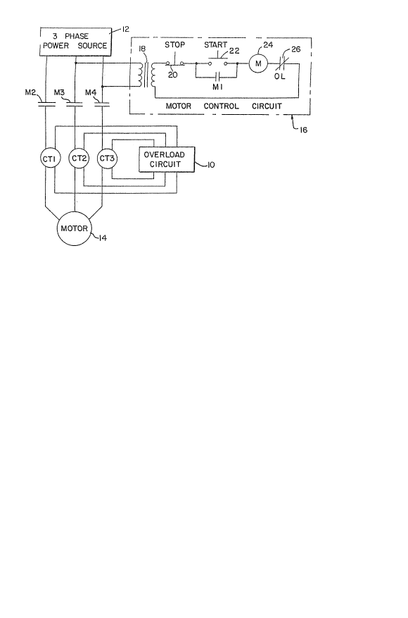
Fig. l is a diagram of a typical three-phase
motor and motor control circuit including an overload
protection circuit in accordance with the subject
invention.
Fig. 2 is a functional block diagram of the
overload protec~ion circuit of Fig. l.
Figs. 3-10 are a detailed circuit diagram of
the overload protection circuit illustrated in Figs. l
and 2.
DETAILED DESCRIPTION OF THE PREFERRED EMBODIMENT
Overview of the System
A power and control system for a three-phase
motor and load is shown in Fig. l. The system includes
an overload protection circuit 10 incorporating the
features of the present invention. A three-phase power
2 ~
source 12 i5 coupled through control contacts r12~ M3
and rl4 and the current transfor~ers CT1, CT2 and CT3 to
the motor 14 in typical manner. Either external or
internal current transformers may be used. A single-
phase start and control circuit lfi is used to control
the supply of power to the motor. Generally, a step
down transformer 18 is used to reduce the power from
the power source (typically 208-600 volts AC) to 120
volts AC. A normally closed STOP button 20 s provided
to break the circuit and manually shut off the power
.supply to the motor. To start up, the normally open
START button 22 is closed, energizing the coil 24 and
closing contacts Ml, M2, M3 and M4. Contact Ml
interlocks the control circuit in order that contacts
M2, M3 and M4 stay energized unless the control circuit
is opened at the STOP button 20 or is opened by the
opening of the normally closed overload contacts 26.
The overload circuit 10 of the present
invention is connected to the secondaries of the three
current transformers CTl, CT2 and CT3 for monitoring
the load current to detect the presence of an overload
condition. When a predetermined overload condition is
present, the overload circuit 10 is activated to open
contacts 26 and shut down the power supply to the motor
1~. After certain events have occurred, the contacts
26 will reclose to permit starting the motor. The
overload circuit of the present invention incorporates
a multiplexing scheme which permits monitoring each of
the three power phases. Use of the multiplexer permits
continuous sequential scanning of the load on each
phase. The gain on the output of the multiplexer is
adjustable to permit use of the overload circuit with a
plurality of motor sizes.
An expanded functional block diagram of the
overload control circuit is shown in Fig. 2. As there
3 ~
shown, a signal converter 52, ~4 and 56 is provided and
coupled to each of the current transEormers CTl, CT~
and CT3, respectively. The converters convert the
current at each phase of the motor into a filtered d.c.
S signal for input to the multiplexer ~5. The
multiplexer U5 continuously sequentially scans the
outputs of the converter circuits to monitor the load
level on each o~ the three phases of th0 motor
windings. The three monitored signals produced by the
converter circuits 52, 54, 56 are input to ~he
multiplexer where they are comhined to produce a single
output which preserves the indepenci~nt identity of each
of the three inputsO This combined signal is input to
a gain control circuit 60 where the current gain range
can be set in accordance with the load specifications
for each particular motor 1~. An important aspect of
the invention is the ability to attach a digital volt
meter to the external ports Pl of the gain control
network 60 in order to externally read the gain set by
the adjustable gain control circuit. This provides an
inexpensive yet accurate way to select and control the
gain on the overload circuit.
The output of the gain control network is
introduced into the microprocessor ~1. When the output
of the gain control exceeds the overload condition, the
microprocessor senses this and initiates an over;oad
trip subrou~ine. The trip delay circuit RP2 controls
the activation of the trip signal, requiring that the
overload condition be present for a specified period of
time before the trip signal is activated. The trip
delay circuit also provides for the attachment of an
external meter to ports P2 to determine the trip delay
range. This permits accurate yet inexpensive setting
of the delay in accordance with the motor
3S specifications and operating parameters.
-9 2~
If the overload condition is present for the
de~ined period of time, the trip seque~ce is initiated,
and a trip signal is output by the microprocessor to
the relay drive circuit 62. The relay dLive circuit is
S coupled directly to the overload contacts 26 (Fig.
I). When the trip signal is present, the normally
closed contacts 26 are opened and the motor is shut
down.
The reset delay circuit RP7 controls the
period o~ time during which the motor control circuit
cannot be reactivated after shutdown to start motor
14. The reset delay circuit is adjustable from a
minimum time of five minutes to a maximum time of 120
minutes, as specified by the motor manufacturer. The
actual reset time is dependent on this setting, the
trip/time curve, and the previous load conditions
(thermal memory data).
Readouts are provided at LEDl and LED2 to
identify at all times what mode the overload circuit is
in, e.g., ready, fault detected, trip routine
initiated, and delay cycle initiated.
A test circuit 57 is coupled to one of the
outputs of the signal converters (as shown, the phase
three signal converter 56) to provide a simulated
overload condition for testing the operability of the
overload circuit when the motor 1~ is de-energized and
no current is flowing through current transformers CT1,
CT2 and CT3. When the test switch S~3 is closed, the
test circuit provides to the multiplexer U5 a test
voltage sufficient to signal an overload and provide a
trip condition output from the gain control circuit 60
to the microprocessor Ul. This initiates the trip
condition subroutine in the microprocessor to test the
operability and time period of the trip delay and the
-~ reset delay circuits RP2 and RP7, respectively. The
Z ~ IJ ~ ~
relay drive 62 responds to the test circuit in the same
manner as it would to an actual overload condition.
Once the test overload reaches the reset delay stage,
the test sequence is completed and the system can
either be manually or automatically reset, depending on
the option shown.
The watch dog circuit 66 provides two
functions. First, it contains the power-on/reset
sequence that allows the microprocessor to initialize
prior to operation. This is a time delay sequence
initiated after the power supply to the microprocessor
Ul is turned on, wherein the microprocessor is
permitted sufficient time to go through its
intialization sequence prior to being powered up and
operational. In addition, once the microprocessor is
operational, the watch dog circuit monitors an output
signal from the microprocessors to make certain the
software code is being properly executed.
An optional remote reset circuit 64 is
provided to allow the user to reset the system upon
completion of an overload detection, trip and delay
sequence by supplying a 120 VAC signal. The reset
circuit is isolated from the overload circuit by an
optical coupler, which is further described in the
detailed description of the circuit herein.
An optional memory circuit 63 is provided in
conjunction with the optional computer interface
circuit 70. The optional interface circuit 70 is a
standard computer interface such as, by way of example,
the Cutler-Hammer E-Link RS485 computer interface
presently available from the assignee of the subject
invention. The computer interface permits the overioad
circuit to be coupled to a computer control system.
This permits entry by the computer of the various
conditions and parameters to be monitored and allows
for automatically setting the programmable features of
the microprocessor via computer control.
~n optional powe~-off circuit 72 is also
illustrated. This feature monitors the condition of
the overload relay system just prior to a power loss.
For example, if the power supply to the microprocessor
is cut off, the optional power off circuit will detect
whether the shut down occurred during normal operating
conditions or during an overload sequence. In the
event that the shut down occurred during normal
operating procedures, upon restoration of power to the
microprocessor the power-off circuit will signal to the
microprocessor that an overload condition was not
present at the time of shut down. This will eliminate
the motor energization delay sequence. In the event
that the shut down occurred during an overload
condition, upon restoration of power to the
microprocessor the power-off circuit will signal that
the shut down occurred during overload. In this case,
the delay sequence will be activated before the motor
can be energized.
Detailed Description of tha Circuit
Figs. 3-lO are a detailed circuit diagram of
the overload circuit lO illustrated in Figs. 1 and 2.
Standard engineering nomenclature and symbols are
used. Throughout the circuitry in Figs. 3-10, the pin
designations of the manufacturers are consistently
used. For clarity, some of the signal lines have been
"bundled" to simplify the drawing. Specifically, lines
hl-h4, il-i8, kl-k5 and ccl-cc4 are shown as bundled in
Fig. 6. Each reference numeral in each of these
bundles represents a separate and distinct signal line
in the drawing, e.g. hl is always separate and distinct
from h2, and so on.
-12- ~ 3 ~, ~
1. Power ~upply
Turning now to Fig. 3, the overload circuit
o~ Figs. 1 and 2 is driven b~ the power supply circuit
there shown. The power supply utilizes the 120 volt AC
power available from two lines of typical three-phase
power supply 12, as connected at terminals ~B2 and
TMB2. At the option of the l~ser, an external 120 VAC
power supply can also be used. A step down transformer
Tl reduces the 120 volt source to 8 volts rms. In the
drawing, the transformer Tl is an ST3/SPW402
transformer manufactured by Permagnetics. The diode
bridge defined by diodes Dll, D12, D13 and Dl~ produces
a full wave rectified 8 volt d.c. voltage partially
filtered by electrolytic capacitor C7. The ceramic or
polyester capacitors Cl, C12, C18, C24 and C32 are for
noise suppression. The 8 volt d.c. signal at node 6
has substantial ripple which is used for non-critical
components such as the indicators LEDl and LED2 and the
relay drive 62. Wherever this source is used, it is
designated by 8VCCA. This voltage is filtered further
by the electrolytic capacitors C8 and C23 to provide a
smooth clean 8 volt d.c. signal at node 8, which is
used by critical components. Whenever this source is
used, it is designated by 8VCCB. Diode D16 is present
to isolate the 8VCC~ source from the 8VCCB source.
Voltage regulator VRl (LM78LOSACM, ~ational
Semiconductor) provides a constant clean 5 volt d.c.
signal designated 5VCC at node 7. Capacitor C33
provides filtering when current surges occur. The
voltage regulator VR2 (~EF02HCSA, Raytheon) and
calibrating potentiometer RP3 provide a calibrated 5
volt d.c. reference voltage ttolerance within 1%) 5VREF
at node 9. RP3 provides feedback for VR2 to maintain 5
volts d.c.
.
Also as noted ;n the remaining drawings, the
8VCCA signal is monitored for shutdown since the signal
is less filtered than the 8VCCB or either 5 volt
signals arld, therefore, 8VCCA will drop out faster than
the others which are dependent upon discharge of the
various capacitors.
Node 5l is the system ground node to which
all the grounds are tied. Ground nodes and associated
terminal tie-ins are represented by standard symbols
and for purposes of this description are common
throughout the circuit.
2. Signal Converters
As shown in Figs. l and 2, the overload
circuit lO is connected across the output coil of each
current transformer CTl, CT2, and CT3. Referring now
to Fig. 4, in the preferred embodiment, internal
current transformers 30a, 30b, 30c are included for
each phase. The primary 32a, 32b, 32c of each current
transformer CTl, CT2, CT3 is the respective line from
motor 14 and is, of course, connected directly to one
phase of the power source l2 through the contacts M2,
t13 or M4 (Figs. l and 2). The secondary windings 34a,
34b, 34c are passed through the respective internal
current transformers 30a, 30b, 30c and define the
primary windings 36a, 36b, 36c thereof. Each signal
converter 52, 54 and 56 of the overload circuit lO is
connected across the secondary winding 38a, 38b, 38c of
the respective current transformer 30a, 30b/ 30c.
In order to understand the operation of this
section of the circuit, it will only be necessary io
describe a signal converter connected with one phase
as the remaining two phases operate in identical
manner. Using converter 52, the secondary winding 38a
is connected across a standard ~AV99 diode bridge D4,
D5 to produce a full wave rectified voltage at node
40. An adjustable potentiometer RP6, with resistors
R31 and R32, is connected at node 40 in parallel with
S the diode bridge to create a burden for the current
transformer 30a to produce a voltage signal which can
be adjusted to match the signals from the other current
transformers 30b, 30c. Voltage output is then limited
through the MMBZ5240B Zener ~iode D21 to provide a 10
volt d.c. maximum voltage at node 46. Resistors R23
and R54, capacitors C30 and C3, and the TLC27M7CD
operational amplifier U4B define a two-stage low pa~s
filter for current transformer 30a. This filter
configuration has a center operating frequency of
approximately 100 Hz. The remaining converter circuits
54, 56 are comparable to the above-described converter
circuit 52, with components D6, D7, R30, R29, RPS, D22,
R22, R52, C29, C4, U6B, R51 comparable respectively to
D8, D9, R28, R27, RP4, D17, R21, R50, C28, CS, U6A,
R49, which axe comparable respectively to D4, D5, R32,
R31, RP6, D21, R23, R54, C30, C3, U4B, R53.
Thus, as shown, the respective voltage output
of the three current transformers CTl, CT2 and CT3 is
present at nodes 46, 48 and 50. All are referenced to
ground at node 51. The low pass filters for current
transformers CT2 and CT3 include the TLC27M7CD
operational amplifiers U6B and U6A, respectively. The
filtered output of the amplifiers U4B, U6B and U6A are
introduced into the multiplexer circuit US (Fig. S)
through the respective current limiting resistors R53,
RSl and R49 and via lines d, e, and f, respectively.
The capacitor C27 is for noise suppression.
-15
- 3. ~lultiplexer
As shown in Fig. 5, the 4052D multiplexer ~5
manu~actured by Nation31 Semiconductor is a dual, four-
channel, two-output circuit. The two ol~tputs are at
pins 3 and 13 and the inputs are at pins 1, 2, 4, 5, 6,
11, 12, 14 and 15. The outputs of amplifiers U4B, ~6B
and U6A are introduced into the multiplexer U5 at pins
12, 14 and 15 via lines d, e, and f. The reference
voltage is tied to the fourth input pin 11. The
reference voltage is generated by using the voltage
divider created by the resistor R37 and the resistor
R38 (Fig. 4). This provides a gain adjustment
reference signal for the outputs from the amplifiers
U4B, U6B and U6A. For present purposes, only one
output of the multiplexer is required and this is taken
at pin 130 Also, the remaining inputs on pins 1, 2, 4,
5 and 6 are rendered inert by shunting to ground.
The output of the multiplexer at pin 13 is
directly related to the instantaneous voltage level
read on the continuously scanned inputs from lines d,
e, and f at respective pins 12, 14, and 15 of the
multiplexer. By continuously scanning the inputs,
using the 4052D multiplexer sho~n, approximately 10
readings or samples per input are taken every 16
milliseconds. These readings are combined and are
outputted on pin 13. As is typical, the multiplexer
output is serial in nature. Thus, the identity of each
input is preserved, though combined into a single
output. By way of example, samples 1, 4, 7, 10
represent the input on pin 12. Samples 2, 5, 8, 11
represent the input on pin 14. Samples 3, 6, 9, 12
represent the input on pin 15. In this manner, the
distinct identity of the three independent signals is
preserved in the combined signal. This gives a very
accurate picture of the current load on motor 14 and
-16- ~ ~ iL ~
pEovides for accurate c)nd e~ficient monitoring by the
overlead circuit. Capacitor C17 is for noise
suppression.
4. Gain Control
The output on pin 13 of the multiplexer is
tied to the gain control circuit 60 (Fig. ~) at pin 3
of the TLc27Mcn operational amplifier U4A. The lM ohm
resistor 26 provides a ground reference for the
multiplexer output signal which is then introduced to
the input pin 3 of the amplifier [J~A. Output pin 1 of
amplifier U4A is tied to pin 13 o the connector Fl.
This is mated with pin 13 of the mated connector Ml
(Fig. 6. Note, all pins on connectors Fl and Ml
correspond). The pin 2 input of the amplifier U4A is
tied to the lOK ohm adjustable potentiometer RPl (also
Fig. 6) through pins 12 of the connectors Ml and Fl.
The lK ohm resistor R6 provides current limiting
through diode Dl9 to protect the microprocessor Ul
(Fig. 6). The output on pin 1 of the amplifier U4A is
tied to node 61 (Fig. 6) between the resistor R6 and
the potentiometer RPl via pins 13 of the connector Fl
and Ml. This provides for adjustment of the gain on
the amplifier U4A based on the voltage reference
introduced at pin 11 of the multiplexer U5 (as herein
described). ~s shown, the 5VREF reference voltage is
divided by the resistor divider network R38 and R37.
In the preferred embodiment, this network supplies
approximately .45 volts. The amplifier V4A is designed
to permit a gain of from 1 to 6, or an output of about
1/~ volt to about 3 volts in the FLA adjustment mode.
The potentiometer RPl (at node 61) is tied to
pins 1 and ~ of the amplifier U4A through pins 13 and
12 of the connectors Ml and Fl. The output signal
,
-17~
present at node 61 is current l;mited by the lK ohrn
resistor R6 and is tied to the microprocessor at pin
38. Pins Pl (Fig. 6) provi~e a test point where the
digital volt meter can ~)e inserted into the circuit in
order to set the operational amplifier gain. Resistor
R36 is present to prevent loading the amplifier U~A
when the meter is connected to pin Pl. Resistor R15
(Fig. 5) is a current limiting device. Capacitor C6
(Fig. 5) is for noise suppression.
5. Relay Circuit
Turning now to the relay circuit 62 (Fig. 5),
the ~IMBD9l4 diode D23 is a free wheeling diode to
protect the drive circuit U2 (Fig. 7). This assures
that when the relay Kl is turned off, there is a
current flow path so the voltage at pin 16 of relay Kl
does not go above the voltage rating of driver U2,
preventing blowing of the relay drive transistors.
Resistors R3 and R7 (Fig. 5) drop the eight-volt power
supply voltage 8VCCA to five volts to drive the relay
circuit. It will be understood that the choice of
relay is arbitrary and the power supply for the relay
will be consistent with the requirements for the relay
selected. Pins 5, 8, 9 and 12 of the relay K1 are
connected to the relay contacts such as overload
contacts 26 (Fig. 1) through terminal block TBl. The
relay pin 1 is tied to pin 12 of the driver U2 through
pins 2 of the connectors M1 and Fl and line M. Pin 16
of the relay Kl is tied to pin 54 of the microprocessor
Ul (Fig. 6) via pins 12 and 5 of driver U2 (Fig. 7) and
line Kl. The relay circuit 62 is energized by the
output from microprocessor pin 54.
Specifically, when the relay transistor Q2 is
turned ON, the signal at pin 16 of the relay Kl is
pulled LOW. This closes the circuit b~tween pins 5 and
8 of the relay ~1 to close the overload contacts 26
connected to terminal block TBl of the relay Kl.
Similarly, the circuit between pins 9 and 12 of the
relay Kl is opened to open the associated contacts at
the terminal block TBl. When the microprocessor
outputs a signal at pin 54 (~ig. 6) and thereby to pin
16 of the relay Kl ~Fig. 5), this signals an overload
trip conditionO Pin 54 goes IOW~ driving pin 16 of the
relay ~1 LOW to de-energize the relay, reversing the
state of the contacts to shut down the motor 14 by
opening up the start and control circuit 16. In the
illustrated embodiment, the contacts tied to pins 8 and
5 correspond to the overload contact 26 of Fig. l. The
remaining contacts tied to pins 9 and 12 are generally
reserved for alarm signals and the like.
6. Watch Dog Circuit
The watch dog circuit 66 is shown in Fig.
8. This circuit provides two distinct functions. The
first is a power-on reset function defined by the
LM939D comparator U7B and the RC network R19, R2~, Rl2,
C22 and the MM3D914 diode Dl8. Resistor Rl9 is 10K
ohm, R12 is 750K ohm and R20 is 33.2K ohms. The output
pin 7 of the comparator U7B is tied directly to the
reset pin 31 of the microprocessor Ul (Fig. 6) via line
a. In normal operation, the five volt supply voltage
5VCC is applied to the voltage divider circuit Rl9 and
R20, and from the voltage divider to pin 6 of the
comparator U7B. Ramping up or charging is also
provided on pin 5 through the RC network consis~ing of
resistor Rl2 and capacitor C22. As the capacitor C22
charges up, the voltage slowly rises on pin 5. When
pin 5 goes higher than pin 6, the output of pin 7 goes
: . ' ' ' '
~ ~3 ~ v
- 1 9 -
~IGH and the microprocessor is in the operating mode.
The delay yrovided by RC circuit R12, C22 permits the
microprocessor to complete its initialization cycle
once it is powered up. The power on reset circuit time
delay ass~Jres that the microprocessor has time to reset
before it is in the operating mode.
As long as the output on pin 7 is LOW, i.e.,
before reset, the diode D24 holds the signal at pin 2
of comparator U7A down as well. While pin 2 is LOW,
the charge up of capacitor C13 is prevented. This
keeps the output pin 1 of co~lparator U7~ HIGH, because
the voltage on pin 2 is lower than the voltage on pin 3
as produced by the voltage divider network Rll and
R9. When the output on pin 7 goes HIGH, capacitor C13
is charged up by the 8VCCA supplied through diode D20
and is tied to pin 3 of amplifier U7A through resistor
R9. Diode D20 prevents the supply voltage from
exceeding 8 volts. When the charge on capacitor C13
exceeds the level on pin 3 of comparator U7A, pin 1 of
comparator U7A goes LOW. This pulls the M~1BD914 diode
D3 (Fig. 7) to ground via line b. This drives the
signal on diode D3 from pin 5 of the driver chip U2
through the current limiting resistor R40, rendering
the driver output at pin 12 operative. The driver
circuit in the illustrated embodiment is an MC1413D
driver manufactured by Motorola. The output of pin 12
of the driver U2 is tied to pins 1 and 1~ of relay
circuit Kl through pins 2 of connectors Ml and F1
(Figs. 5 and 6). When a fault condition occurs, pin 54
of the microprocessor Ul (Fig. 6~ goes LOW, as will be
explained. This pulls pin 5 of driver U2 LOW, and this
is output at pin 12 of the driver U2, de-energizing the
relay transistor Q2 at pins 1, 16 of the relay circuit
Kl (through pins 2 of connectors M1 and Fl) to reverse
the state of the relays.
-20- ~6~
Capacitor C10 (Fig. 8) is ~or noise
suppression. Resistor R17 is a current limiter for
delaying the charge up of capacitor C13. Resistor R13
is a pull-up resistor to pull up pin 7 of comparator
U7B to a fllll 5 volts when HIGH. Resistor R55 is a
feedback resistor for hysteresis.
The output of the comparator U7A on line b
(Fig. 8) is also tied to diode D25 (Fig. 7). Pin 4 of
driver U2 is pulled LOW through resistor R61 for
current limiting when pin l of the comparator U7A is
LOW. This causes pin 13 of driver U2 to go ilIGH and
de-energizes the green system ready light LED2 (Fig. 7)
which is connected to pin 13 of the driver U2 through
the current limiting resistor R16. At the same time,
when pin 1 of comparator U7A is LOW, the red LEDl (Fig.
7) is energized through the current limiting resistor
R4 and diode D25.
The second function of the watch dog circuit
66 is the watch dog function. To provide this
function, the input to pin 1 of driver U2 (Fig. 7) is
taken from microprocessor pin 58 (Fig. 6) through the
capacitor Cl9 via line k5 (Fig. 7). The capacitor Cl9
is present to smooth out any spike due to the
transition of the microprocessor from a disabled state
to a ready state, preventing the spike from being
applied to pin l of driver U2, thereby preventing a
false input signal to the watch dog circuit if the
microprocessor is stuck HIGH. The corresponding output
signal on pin 16 of the driver U2 (Fig. 7) is fed on
line c (Fig. 7 to Fig. 8) back to pin 2 of comparator
U7~. This keeps the signal on line c LOW and keeps
from charging capacitor C13, holding the comparator U7A
output signal on pin l HIGH.
Lhus, once the microprocessor Ul (Fig. 6) is
in the operating state and pin 7 of comparator U7B goes
-21~
HIG~I, the system continues in an operating mode as long
as the microprocessor produces an output .signal at pin
58. This keeps pin 16 o~ driver U2 LOW and a L~W
signal on line c, which keeps capacitor C13 (Fig. 8)
from charging. This maintains the output on pin 1 of
the comparator U7A HIGH. ~hen a malfunction or fault
occurs at the microprocessor, altering the output on
pin 58, the watch dog circuit is operative to shut down
the system. This occurs because pin 1 of the comparator
U7A (Fig. 8) goes LOW, pulling pin 5 of driver U2 LOW
through diode D3 and resistor R40. This changes the
state of the signal on pin 1.2 of the driver U2 and
since this is tied to pins 1 and 16 of the relay Kl
(Fia. 5), the relay transistor Q2 is operative to
deactivate the contacts.
As shown, the output on pin 1 of the
comparator U7A (Fig. 8) is also connected via line b
directly to the red light emitting diode LEDl (Fig. 7)
through diode D26. Whenever the output on pin 1 of
comparator U7A goes LOW, the light emitting diode LEDl
is energized.
As stated, the output on pin 13 of driver U2
~Fig. 7) is directly connected to the green system
ready light emitting diode LED2 (Fig. 7). Whenever the
signal on pin 13 goes LOW, this light is energized. As
described, this occurs whenever the input to pin 4 of
driver U2 is HIG~, which occurs whenever the output on
pin 1 of comparator U7A (Fig. 8) is HIGH and the diode
D25, through resistor R61, is operative to pull pirl 4
of driver U2 LO~.
7~ Test Circuit
The test circuit 57 is shown in Fig. 4. As
there shown, the pin 1 output of signal converter
-22-
amplifier U6A is tied to the collector of the ~1MB'r3906
PNP transistor Ql through resistor R49. The driver of
transistor Q1 is tied to pin 7 of the microprocessor ~1
(Fig. 6) via line s, through resistor R42 and pins ll
of connectors Ml and Fl. Test switch SW3 (Fig, 9) is
tied to pin 5 of the microprocessor Ul (Fig. 6) via
line aa. Test switch SW3 (Fig. 9) is normally open and
includes the antibouncing capacitor C31 (Fig. 9) to
eliminate sporadic signals. The resistor R14 is
norrnally tied to ground to keep microprocessor pin 5
LOW. When the test button SW3 is depressed and closed,
pin S goes HIGH and the microprocessor test routine is
activated. This generates a flashing signal at pin 57
of the microprocessor Ul, which is sent to pin 2 of
driver U2 (Fig. 7) via line K4, activating pin 15 of
the driver U2, whereby the red LEDl starts flashing.
Resistor R41 (Fig. 4) is used to keep
transistor Ql OFF until pin 7 of the microprocessor Ul
goes LOW. Resistor R42 provides current limiting on
pin 7 of the microprocessor. When pin 7 of the
microprocessor goes LOW, transistor Ql is turned on to
supply the 5 volts from the test circuit 57 to pin 11
of the multiplexer (Fig. 5), via line f, for simulating
an overload condition.
Also, at this time, the subroutine drives
pins 10 and 8 of the microprocessor Ul (Fig. 6) HIG~.
These signals are transmitted to pins 9 and 10 of the
multiplexer (Fig. 5) through pins 9 and 10 of the
connectors Ml, Fl. This signals the multiplexer to
monitor pin 11 and generate the pin 11 signal as output
on the multiplexer pin 13.
After a programmed delay, p~n 57 of the
microprocessor Ul (E'ig. 6) goes steady HIGH and the
light LEDl (Fig. 7) turns steady red, signaling an
overload trip condition. At this timel the signal on
-23 ~ v
pin 55 o the microprocessor oscillates HIGH and LOW,
and this signal is sent via line k2 to driver U2, pin
4, activating driver pin 13 to cause the green LED2
(Fig. 7) to start flashing, indicating that the
S microproc~ssor Ul is calculating when reset will be
operational. At that point, the subroutine is
complete, the system is reset and the test sequence is
cornplete.
8. Trip Delay Circuit
The delay circuit is shown in Fiy. 7 and
includes the lOk potentiometer RP2 which is tied to the
microprocessor U1 (Fig. 6) at pin 37 via line o and is
used to set the trip delay time (or overload class).
~5 Open pins P2 and P13 permit external monitoring of the
trip time. This permits the user to read the voltage
drop across the line and adjust it by adjusting the
potentiometer RP2 to accommodate the time/trip curve
for each particular motor. Capacitor C9 is for noise
suppression. Resistor Rl is provided for current
limiting when the meter is attached to pins P2, Pl3.
9. Reset Time Circuit
Reset time circuit is illustrated in Fig. 7
~ and includes the lOK potentiometer RP7 which is tied to
pin 40 of the microprocessor Ul (Fig. 6) via line p.
The resistor R33 sets the lower boundary of the reset
time to five minutes, so that the reset delay cannot be
inadvertently set to zero. Capacitor C21 is for noise
suppression.
-2~
10. The 11icroprocessor
The 7~10Cl~G or masked microprocessor ~1
manufactured by NEC Flectronics is shown in Fi~. 6. As
used in the preferred embodiment, it includes the dip
switch programming shown in Fig. 9 to provide enhance~
product protection. This is achieved by cutting small
open points or traces in the signal paths in the
circuit board and inserting the dip switch SW2 at that
point. Normally all of the traces are held to ground
as shown at pins 9-16, and the traces are bro~.en at
pins 1-8 of the dip switch. The dip switch is soldered
into the circuit board at that point to close the
opening or trace. In series with a dip switch is the
RPACKl unit which pulls all dip switch lines l-]IGH if
the dip switch is OFF, and LOW if the dip switch is ON
or in the normal condition. Pins P25, P26, P27, P28,
P29, P30, P31 and P32 are test points to determine
whether the dip switch is open or closed on each
respective line. The dip switch SW2 and RPACKl are in
series. The corresponding pins 5, 6, 7 and 8 of the
dip switch SW3 and RPACKl are tied to pins 63, 62, 60
and 59 of the microprocessor (Fig. 6) via lines i4, i3,
i2 and il for ac~uating options described but not shown
herein. Resistors RPACK l provide pull-up for the
microprocessor inputs on pins 2, 3, 4, 59, 60, 62r 63,
64, 65, 66 and 67 via pins 9-16 and lines x, y, z and
il-i8 (Fig. 9).
Jumper JPl (Fig. 9) controls the power-off
circuit 72 (Fig. lO)o Jumper JP2 controls the optional
memory 68 (Fig. 9), and jumper JP3 controls the
optional RS485 computer interface 70 (Fig. l0). When
the optional circuits are used, the jumpers are cut or
opened. The jumpers are shown closed here to
illustrate the operability of the circuit when these
-25- 2 ~
options are not used. When closed, the jurnpers are all
tied to ground thr~ugh jurnper terminal JP6 (Fig. 6).
Power is s~pplied to pins l and 47 o~ the
microprocessor Ul (Fig. 6). The capacitor Cl5 is a
noise-suppression capacitor. Resistor R25 is a pull up
resistor tied directly to pin 30 of the microprocessor
to continuously pull it HIG~, indicating use of
internal mernory. Resistor 24 is tied to microprocessor
pin 28 and provides an instantaneous reset whenever
line n on pin 28 of the microprocessor is pulled to
ground, pulling it HIG~ whenever power is supplied to
the microprocessor, independently of the sequence in
the software code.
Note that pin 28 of the microprocessor is
connected via line n through pins ll and 6 of the
driver U2 (Fig. 7) to the capacitor C44 and reset
button SWl (Fig. 7). This permits use of switch SWl to
generates a momentary pulse to reset the
microprocessor. ~hen power is cycled very rapidly and
the system does not reset itself, then reset switch SWl
can be closed to manually actua~e the reset cycle by
generating a momentary pulse to pin 28 to reset the
microprocessor Ul.
The 12 MHz microprocessor crystal Xl (Fig. 7)
is tied to the microprocessor pins 33 and 34 (Fig. 6)
via lines r and s. The capacitor Cl4 (Fig. 7) is for
noise suppression on the analog reference input pin 45
and is tied thereto via line t. The lOK ohm resistor
R34 and the 3.32K ohm resistor R35 (Fig. 7) form a
voltage divider and are tied to the microprocessor Ul
(Fig. 6) at pin 39 via line u to monitor the 8VCCA
voltage signal through diode ~lO. When power is lost,
the microprocessor is programmed to recognize this and
initiate a safe shutdown~ The diode DlO is clamped to
5 volts to assure that the microprocessor is not
destroyed by the presence of an overvoltage condition.
-26- ~ ~3 ~
In typical operation, pins 1 and 47 provide
power to the microprocessor ~1, see Figs. 6.
Microprocessor pin 2 is connected to jumper JP3 (Fig.
9) and when the input is LO~, i.e. the jumper is closecl
and tied to g~ound, the microprocessor will not go
through the computer interface communication
subroutine. When the jumper is cut and goes HIGH, the
microprocessor will go through a communication software
subroutine and communicate with the optional RS485
computer interface circuitry 70. In like manner, pin 3
is connected to jumper JP2 (Fig. 9) and when pulled
HIGH, the subroutine to communicate with the optional
memory circuit 70 is engaged. When pin 4 is pulled
HIGH, jumper JPl engages the optional power of circuit
72.
Pin 5 is connected to the test switch SW3
(Fig. 9) via line aa. When the test switch is closed
and power is supplied from the 5VCC power source, the
input on pin 5 goes HIGH and, if at this time no
current is passing through the current transformers
30a, 30b, 30c, a simulated overload subroutine will be
activated by the microprocessor. As previously
described, this causes pin 7 to go LO~. As stated, pin
7 is tied to transistor Q1 (Fig. 4) through pins 11 of
the connectors M1 and Fl (Fig. 5). This causes the
transistor Q1 (Fig. 4) in the test circuit 57 to turn
ON, supplying a 5 volt signal to pin 15 of the
multiplexer U5 (Fig. 5) via line f This signal
simulates an overload condition on the output pin 13 of
the multiplexer U5. This output is tied to pin 38 of
the microprocessor U1 via the gain amplifier U4A, pins
13 of connectors Ml anf Fl and gain adjustment
potentiometer RP1 (Fig. 5). Once this simulated
overload condition is present on pin 38 of the
microprocessor, the subroutine generates a "flashing"
-27-
signal on pin 57, i.e., the signal oscillates ~rom ~IG~I
to LOW. Pin 57 is tied to pin 2 of the driver U2 (~ig.
7) and the ~lashing signal ca~ses red L~Dl to flash on
and off, as previously described. At the end of the
flashing sequence, the output on microprocessor pin 57
is shifted to continuous HIGH and the red LEDl is
steady ON. At this time, the output on microprocessor
pin 54 is switched to LOW, which turns off the relay Kl
(Fig. 5) via the driver ~2 (Fig. 7) and pins 2 of the
connectors Ml (Fig. 6) and Fl (Fig. 5). Pin 55 is
programmed to oscillate between LOW and HIGH, causing
the green LED2 to flash at each cycle via the driver
U2. When the green LED2 stops flashing, the reset
button SWl can be pressed to reset the overload (or the
overload is automatically reset if the option is
activated by the presence of a HIGH signal on pin 59 of
the microprocessor Ul). At this point, pin 57 goes
LOW, the red LEDl is turned off, pin 54 goes HIGH, and
the relay Kl is energized, signaling the end of the
test sequence.
When the reset switch SWl (Fig. 7) is pressed
and held down, and no current is flowing throuyh
current transformers 30a, 30b, 30c the full load
amperage (FLA) can be adjusted at potentiometer RPl
(Fig. 6). Pin 6 of the microprocessor is connected to
the reset button SWl via line q and when HIGH, pins 8
and 10 are programmed to go HIGH and, via pins 10 and 9
of connectors Ml and Fl, this is introduced into pins
10 and 9 of the multiplexer U5 (Fig. 5). When this
occurs, the designated voltage as determined by the
resistor divider R37 and R38 (Fig. 4) is input to pin
ll of the multiplexer U5 (Fig. 5) via line g. This is
output at pin 13 of tha multiplexer U5 and input at pin
3 of the operational amplifier U4A (Fig. 5). The
output voltage at pin l of operational amplifier U4A
-28- ~t
(also accessible at test point Pl (Fl9. 6) accessible
from the outside) is dependent upon the feedback which
is set by the potentiometer RP1 (Fig. 6) as connected
through pins 12 and 13 o~ the connectors Ml and Fl.
The user may adjust the potentiometer RP1 and monitor
the adjustment at the test point Pl so that the
overload for a particular current range can be
accurately set using the standard formula, where FLA
d.c. volts is equal to three times the current
transformation ratio divided by the motor FLA
current. Once the reset switch SWl (Fig. 7) is
released and opened, pin 6 of the microprocessor U1
~Fig. 6) returns to LOW and the microprocessor goes out
of the FLA adjustment mode. If current is flowing
through the current transformers 30a, 30~, and 30c,
both this function and the reset function are
inactive.
When the overload is tripped and the green
LED2 is not flashing and the red LED1 is on steady, the
overload can be reset by pressing the reset switch SWl,
as described above. At this point, the relay Kl (Fig.
5) is energized via pins 14 of the connectors Ml and
Fl, and LEDl is turned off. Microprocessor pin 28
(Fig. 6) is driven LO~ when the reset button SWl (Fig.
7) is depressed. This function is utilized when the
microprocessor Ul locks up when the 120 volt power
supply is lost and then re-established before the power
supply has gone low enough to allow a normal reset of
the microprocessor. Resistors R2, R4 and Rl6 (Fig. 7)
are current limiting devices. Capacitors C2 and C26
(Fig. 7) are for noise suppression.
Microprocessor pin 37 (Fig. 6) is connected
to the potentiometer RP2 (Fig. 7) via line o and this
analog input is used to set the class of overload from
l to 50 seconds. A digital volt meter may be attached
-29- ~ 3
across open pins P2 and P13 (Fig. 7) to determine the
setting o~ potentiometer RP2. The capacitor C9 is ~or
noise s~ppression and resistor Rl provides current
limiting when the meter is attached.
Microprocessor pin 38 (Fig. 6) is the analog
input for sensing the current which is multiplexed by
the multiplexer ~5 (Fig. 5) and is connected to node 60
(Fig. 6) through resistor R6. As stated, this
multiplexed, combine~ signal is present at multiplexer
U5, pin 13, with gain adjust~ent by amplifier U4A and
is o~Jtputted at pin 1 of amplifier U4A (Fig. S), where
it is introduced, via pins 13 of connectors Ml and Fl,
gain potentiometer RPl, and reslstor R6 to pin 38.
Since the identity of the three discrete inputs is
preserved in the combined signal, the multiplexer is
programmed to redefine the three signals and store each
of them in a designated register.
Pin 39 of the microprocessor Ul (Fig. 6) is
the analog input which senses the presence or loss of
120 volts power by being tied directly to the 8VCCA
source via line u as shown in Fig. 7. Pin 40 of the
microprocessor Ul (Fig. 6) is connected to the
potentiometer RP7 through resistor R33 (Fig. 7) via
line p which is used to calculate the reset time under
a tripped condition as previously described.
Pin 54 of the microprocessor is tied to the
relay Rl (Fig. 5) via pin 2 o~ connectors Fl (Fig. 5)
and Ml (Fig. 6), line m, and pins 12 and S of driver U2
(Fig. 7) and line kl (Figs. 7 and 6). ~in SS is tied
to the green LED2 (Fig. 7) via line k2, as previously
described. As the microprocessor is programmed, when
the green LED2 is ~lashing, it is providing an
indication that the overload is not ready to be reset
after trip has occurred. During this time, the signal
on pin 54 is held LOW and the relay Kl cannot be
_30_ 2~
reset. When the light LED2 goes steady ON t~e relay
can be reset manually or automatically. If the green
LED2 is OFF and the red LE31 is ON, there is a
microprocessor ~ault.
Pin 57 of the microprocessor (Fig. 6)
controls the red LEDl (Fig. 7) via line k4, as
previously described. As programmed, when the red LEI)l
flashes, it indicates an impending overload trip and
when the red LED is on steady, it inicates that the
overload has tripped.
Pin 58 of the microprocessor Ul (Fig. 6)
pulses pin 1 of driver ~2 (~ig. 5) via line k5 to keep
capacitor Cl3 (Fig. ~) discharged thereby preventing
the watch dog timer from tripping the overload relay,
as previously described.
When pin 59 of the microprocessor ~l (Fig. 6)
is LOW, reset of the overload circuit can be performed
as follows: once the overload trips, the user has to
manually push the reset switch SWl (Fig. 7) to energize
the relay kl (Fig. 5) via pins 14 of the connectors l~l
and Fl. When the pin 59 is HIGH and the overload is
tripped, the microprocessor U1 automatically determines
when to reset the overload based upon the reset time as
set at potentiometer RP7 and resistor R33 (Fig. 7), the
overload class setting at potentiometer RP2, and the
prior thermal energy conditions.
The class of overload is determined by the
setting of potentiometer RP2 and the thermal energy
calculated to bring the motor up to speed the previous
time. If the overload circuit detects zero current
through any of the current transformers 30a, 30b, 30c
during start-up of the motor 14, the overload ~ill trip
in 60 milliseconds.
The trip delay time is manually set at
potentiometer RP2, as described. Also, the
-31- 2 ~ 7
microprocessor Ul is programmed to recalculate the trip
delay time ~ased on previous motor operating
conditions. For example, if the motor trips out upon
start-up, a "cold trip" curve in accordance with NEMA
standards (National Electrical Manufactures
Association), is followed ancl the delay time is
automatically altered by the microprocessor. If the
motor trips after achieving l00~ FLA, then dropping
below l00~, then increasing to trip ]evel, the trip
delay time is shorter than the "cold" condition
delay. The microprocessor Ul is programmed to rely on
either the NEMA "cold trip" curve and the N~A "hot
trip" curve, depending on conditions of the rnotor,
wherein the "cold" curve is relied on when the motor is
lS initially powered up and the "hot" curve is relied on
aEter reaching 60% thermal memory.
These features are only active when the
current being sensed by the overload relay has risen
above l00~ FLA and then has gone below 100% FLA. In
the embodiment illustrated, the undercurrent trip
option, jammed delay overload option, phase-loss option
and phase unbalance option may be used or not used, as
desired. The microprocessor Ul is programmed, however,
to utilize these options when desired, and the pin
response for these is as follows:
When pin 60 of the microprocessor Ul is HIG~,
the undercurrent trip option is activated. This
feature causes the overload relay to trip to de-
energize relay Kl when the sensed current falls below
70~ FLA.
Pin 62 of the microprocessor controls the
uncurrent trip delay overload trip time also through
the dip switch SW2. When pin 62 is LOW, the trip time
is 60 milliseconds. When it is ~IIGH, the delay time is
2 seconds.
-32-
Pins 63 and 64 of the microprocessor are used
to set the threshold current when a ja~ is detected.
If the current sensed by the overloacl goes above the
current specified by the jam level, the overload will
trip and the relay Kl will de-energize in the amount of
time selected by the jam delay. When pins 63 and 64
are LOW, the jam funtion is cle-energized. When pins 63
is HIGH and pin 64 is LOW, the jam current is at 108%
FLA. When pin 63 is LOW and pin 64 is HIGH, the jam
current is at 125% FLA. When pins 63 and 64 are both
HIGH, the jam current is at 200% FLA. Pin 65 of the
microprocessor controls the jam delay trip time. When
pin 65 is LOW, the trip time is 60 milliseconds. When
pin 65 is HIGH, the jarn delay time is 2 seconds.
Pin 56 of the microprocessor controls the
phase-loss option and is tied to the PO~ER OF~ timer 72
(Fig. 10) via pins 3 and 14 of the driver ~2 (~ig. 7)
via lines k3 and ee. When pin 66 of the microprocessor
is LOW, the phase-loss option is turned off. If the
loss of any one phase causes excess current to be
sensed in the other two current transformers, the
overload will trip based on the normal trip curve
selected. When pin 66 is HIGH, the phase-loss option
is activated. If the overload detects zero current
through any of the current transformers 30a, 30b, 30c,
the overload will trip and the relay K1 will be de-
energized in 60 milliseconds.
Pin 67 of the microprocessor controls the
phase unbalance option. When pin 67 is LOW, the
feature is deactivated. When pin 67 is HIGH and the
calculated current unbalance exceeds 15% based on the
following equation:
3 ~ h ~
-33-
(MAX. Current) (MIN. Current)
AVG. Current x 100%,
the overload relay will trip and relay Kl will be
deacti~7ated.
The overload can be reset instanteously by
depressing the reset button SWl (Fig. 7) whenever the
overload circuit is tripped in response to undercurrent
trip, jam trip, phase loss or phase unbalance
conditions.
ll. Remote Reset Circuit
Also shown in the preferred embodiment is an
optional remote reset circuit 64 (Fig. 5)~ Pin 3 of
the transistor side of a PC814IA optocoupler ISOl is
tied to pin 6 of the microprocessor Ul via pins l4 and
line q o the connectors Ml and Fl. The reset switch
SWl (Fig. 7) is also connected to node 65, line q ~Fig.
7). ~he four lOK ohm resistors R43, R44, R47 and R48
provide the drive for the optocouplers. The capacitor
C25 is provided for noise suppression. Pins 1 and 2 of
the optocoupler ISOl are connected directly to a 120
volt power source through the terminal block TB3. When
power is supplied across the termimals on block T~3,
the ISOl transistor is turned on and pin 3 of the
resistor produces a HIGH signal on pin 6 o the
microprocessor via pins 14 of the connectors F1 and Ml
(Fig. 6) and line q. This resets the overload circuit
after completion of the reset delay. Capacitor Cl6
(Fig. 6) is for noise suppression.
-34- 2 ~3 ~
12. Memory Circuit
As illustrated, the overload device of the
subject invention includes an optional memory circ~it
68 (Fig. 9). The optional memory circuit 68 includes
an ~lMC93C46M nonvolatile serial memory chip U3
manufactured by National Semiconductor. Typically, the
optional memory circuit would be used in conjunction
with the ~S485 communication net~70rk interface 70 ~ig.
8), or in conjunction with use defined requirements.
The optional memory circuit output pins 7 and 6 are
tied to the microprocessor pins 12 and 11 via lines bb
and hl. The optional memory circuit will perrnit the
user to program various options into the
microprocessor, including, by way of example,
overcurrent, undercurrent, trip delay time, phase
unbalance, jam level, data logging storage, CT
transformation ratio, starting current value, and
potentially overvoltage and undervoltage sensing. Data
is entered into the memory chip U3 pin 3 on 1ine h4 and
output at chip U3, pin 4 on line n into microprocessor
pin 13 (Fig. 6). Pin 3 of the memory chip U3 is tied
to microprocessor pin 14 via line h4, and pin 4 of the
memory chip U3 is tied to microprocessor pin 13 via
line n. The clocking inputs to the memory circuit are
on pins 1 and 2, tied to the microprocessor at pins 16
and 15 via line h2 and h3, respectively.
Microprocessor pin 3 (Fig. 6) is connected to jumper
JP2 (Fig. 9) via line z for activation of the memory
circuit option. When pin 16 of the microprocessor is
HIGH, pin 1 of the memory chip U3 is HIG~, ena~ling the
memory circuit. Typically, the memory chip is to be
loaded via input from a computer coupled to the
computer interface circuitry 70 via microprocessor pins
19, 20, 21 and 22 via lines ccl, cc2, cc3, cc4 (from
the interface, Fig. 5) and pins 13 and 14 via lines n
~8~
-35-
and h4 (to the memory, Fig. 9). Resistors R8, R10 and
R39 (Fig. 9) are current limiters. Capacitor 2~ (Fig.
9) is for noise suppression.
13. Computer InterEace
_
The computer interEace circuitry 70 ( Fig . 8 )
is a stan~ard Cutler-~]ammer E-T.ink RS485 interf.lce,
manufactured by the assignee of the subject invention,
and comprises a pair of SN75ALS176D chips U8 and U9.
The interface circuitry is tied to the microprocessor
(Fig. 6) at pins 19, 20, 21 and 22 via lines ccl, cc2,
cc3 and cc4, as shown. The circuit ~8 is the receiver
for accepting communication from a computer (not shown)
via pins 1 and 2 of the PLUG 6. The metal beads L4 and
lS L5 and the capacitors C40 and C41 are provided for
noise suppression. The voltage drop between the lines
is developed at the .1 microfarad capacitor C35 and
entered into the chip U8 at pins 6 and 7. Resistor R56
is a current limiter.
Circuit U9 is the transmit circuit for
receiving information from pin 19 of the microprocessor
Vl and introducing it to the computer via pins 5 and 6
of PLUG 6. The two resistors R59 and R60 are current
limiting and the capacitors C42 and 43 as well as beads
L6 and L7 provide noise suppression on the trans~itted
data. Resistors R57 and R58 are current limiting
resistors.
The supplemental power supply VR3 is required
to isolate the interface power supply from the
remainder of the overload circuit. The 8VCCA power
source is introduced at pin 8 of the LM78LO5ACM voltage
regulator, as filtered by the capacitor network C38 and
C39. The output at pin 1 of the regulator VR3 is
filtered by the capacitor C44 to produce a smooth 5
..
.
2 ~ J
-36-
volt supply 5VTHM at pin P33 and this is introduced
into pins 8 of circuits U8 and U9, as shown, to drive
the computer interface.
14. Power-Off Timer
The optional power--~ff ~imer circuit 72 (Fig.
l0) monitors the condition on pin 41 of the
microprocessor via line dd. The resistor R5 provides
current limiting for chargin~ up the capacitor Cll
through diode Dl5. When the control power is lost
during a normal mode and everything is operating in the
proper manner, the capacitor Cll is discharged by the
driver circuit U2 at pin 14 via line ee. When the
microprocessor (Fig. 5) senses it is losing pcwer on
lS line u from the circuitry defined by resistors R34, R35
and diode ~l0 ~Fig. 7), pin 57 of the microprocessor
goes LOW, driving pin 3 of driver circuit U2 via line
k4 driving pin 14 of the driver U2 LOW and discharging
the capacitor Cll (Fig. l0). When power is restored,
and current flows through diode DlS (Fig. l0), charging
capacitor Cll.
The instantaneous voltage signal present on
diode Dl5 is also fed directly into the microprocessor
at pin 41 via line dd. The microprocessor reads the
voltage across the capacitor ll to determine if it is
discharged LOW i.e. lower than pin 41 of the
microprocessor, or if it is charged HIGH, i.e. as high
as pin 4l of the microprocessor. Assuming that the
microprocessor recognized a fault before power was shut
off, pin 14 of the driver U2 would not go I~OW and the
capacitor Cll would still be charged. When this
occurs, resistors Rl8, R45 and R46 (Fig. l0) provide a
bleeding effect for the capacitor Cll to discharge at a
predetermined rate. After a predetermined time, the
2~ h
-37-
capacitor Cll would be discharged enough to signal to
the microprocessor that upon control power being
supplied, the motor can be started after a fault
condition. If the time of power loss is shorter
than five minutes, the capacitor C11 will still be
charged. In this case, the microprocessor reads a
voltage across capacitor Cll upon control power being
applied, and starts the reset timing from that point.
l5. The Microprocessor Pro~ram
The functional software statement ~or
operating mieroprocessor Ul follows. The statement is
written in assembly languaye. As written, the program
is broken into six eolumns, reading from left to right
as follows-
l. STNO, whieh is the statement number;
2. ADRS, whieh is the address within the
mieroproeessor C]lip where the function is located;
3. R, which is an error code (not used);
4. OBJE~T, which is the souree statement
written in objeet language suitable to the selected
microprocessor;
5. M, whieh is not used; and
6. SOURCE STATEMENT, whieh is an English
language statement of the statement function;
The program begins at statement No. 52.
Statements 1-52 are not related to the operation of
this invention.
2 ~ J
-38-
52
53 0003 FLTg~1 EOU 03H ;FAULS SATU~ INDICAT~ON:
5 4 1 - FAULI'
; BIT O OV~,OAD
56
57 ; 2 PO~ER FAIL
5 8 . ; 3 LOw I ALARM
59 ~ ; 4 ~AM
; 5 PHASE UNBAL
61 ; 6 PHASE L09S
62 ; 7
63
64 0004 FLTSI'2 eou 04H ;EIIT O
66 0006 ITOTL EC1U 06H ;TOTAL CURRE~T VAL J,O~ E
BrT8
67 0007 ITO~M FOV 07H ;MID 9 BISS
68 oooa ITOTH EOU 08H ;HIGH a BITS
69 0009 IAVCLO EOU 09H ;AVG I LOW PH VAL
OOOA IAVCMD EQU 0AH ; MID PH VAL
71 OOOB IAVCHI EQU 0PH ; HIGH PH VAL
72 000C IAVGP1 E9U 0CH ; PHASE ONE
73 000D IAVGP2 EQU 0DH ; PRASE TWO
74 000E IAVGP3 EQU OEH ; PHASE THREE
76 FF06 ITOTLA EOU 0FF06H ;16 BIT ITOTL ADRESS
77 FF07 ITOTMA EQU 0FF07H ;16 BIT ITOTL MID BITS
78 FF08 ITOTHA EOU OFF08H ;16 BIT ITOTH ADRESS
79
0016 ISUML1 EQU 16H ;PH 1 I SUM LOW
81 0017 ISUMHl EQU 17H ; HIGH
82 0018 ISUMLZ EQU 18H ;PH 2 I 9UM LOW
83 0019 I9UMH2 E9U 1~H ; HIGH
84 001A ISUML3 EQU 1AH ;PH 3 I SUM LOW
OOlB ISUMH3 EQU 1~H ; HICH
86
87 FF16 ISUM1 EQU 0FF16H 16 BIT I SUM PH 1 ADDR
88 FF18 ISUM2 EOU 0FF19H ;16 ~IT I SUM PH 2 ADDR
89 FFlA ISUM3 EQU 0PF1AH ; 16 BIT I SUM PH 3 ADDR
91 0022 . GAINSL EQU 22H ; AMPLIFER CAIN S~TTING
92 0023 GAINSH EOU 23H ;LOW AND HIGH BITS
93 0024 RT~UML EQU 24H ;~ESET TIME 9UM LOW
94 0025 RTSUMH EOU 25H ;RESET TIME SUM HIGH
0026 T~SV~L EOU 2 6H ; TIMESET SUM LOW
-39- 2 3 ~
96 0027 TM9U~i EQU 2711 ; TIMESET SVM HIGi3
97 002~ TSTVAl EQU 28H ;THERMAL 5TART VAL9
98 0029 TSTVA2 EaU 29H
99 002A TRSTVl EQU 2AH ;THER~LL RESET VAI,S
100 002~ TRSTV2 EOU 2BH
101 002C AGAINS EaU 2CH ;AVC GAIN 6ETTING
102 002D UNLDI.Y EOU 2DH ; UNDER I TRIP D~LAY
103 002E JAMDLY EOU 2EH ;TRIP TIM~ DELAY VAL
104 002E HTLO':S EOU 2FH ;HEAT LOS9 VAL
0 105
106 FF22 GAINSM EoU OFF22H ;16 BIT AMP GAIN 9UM A~
107 FF24 RTXUM EaU 0EF24H
10a FF26 TIMSUM EQU OFF26H ;16 LIT TlMESE'r ~DD~
109 FF28 TSTVi~ EQU OFF28H ;16 ~IT THE~ ST~nT -
110 ~F2A TRSETV EaU 0FF2AH ;16 BIT THER~AL RESET
111 ;
112 0031 TIMSET EOU 31H ;600 ~FLA TRIP TIME VAL
113 0032 PWRVAL EQU 32H ;POWER VAL LON
114 0033 PWRVAH EQU 33H ;POWER VAL HIGH
115 FF32 PNRVAA EOu OFF32H ;16 BIT PWR VAL ADDR
116 0034 PW~AVG EQU 34H ;LINE POWER AVG
117 0035 TITOTL EQU 35H ;ITOT AT TEST START
118 0036 TITOTM E9U 36H
119 0037 TITOTH EaU 37H
120
121
122 0050 TIM01 EOU 50H ; RESET COUNTER
123 0051 TIM02 EQU 51H ; O.5 SEC TIMER
124 0052 TI~S03 EQU 52H ; JAM DELAY COUNTER
125 0053 TIM04 EQU 53H ; PH UN3AL COUNTER
126 0054 TIM05 EQU 54H ; PH LOSS COUNTER
127 0055 TIM06 EQU 55H ; SETUP TIMER
128 0056 TIM07 EQU 56H ; CYCLE COUNTER
12g 0057 TIM08 EQU 57H ; 0.01 SEC COUNTER
130 0058 TI~S09 Eau 58H ; UP TO SPEED COUNTER
131 005g TIM10 EQU 59H ; UNDER I COUNTER
13Z 005A TIMll EOU 5AH ; PWR FAIL COUNTER
133 005B TIM12 EQU 5BH ; STAAT / STOP COUNTER
134 005C TIMl~ EaU 5CH ; TEST CYCLE START COUN
135
136 0060 TSTORl E9U 60H ;SEMPORARY STOR LOC 1
137 0061 TSTOR2 EQU 61H ; 2
138 0062 TSTOR3 EOU 62H ; 3
139 0063 TSTOR4 ÆQU 63H ; 4
140 0064 TSTOR5 EQU 64H : 5
141 0065 TSTOA6 EQU 65H ; 6
` -40- 2 ~
142 0066 TSTOR7 EO~ 66H ; 7
143 0067 TSTOR8 EOU 67U ; 8
144 EF60 TS~Rl EQU 0FF60H ;16 BIT TEMæ 9TO~ LOC A~
145 FF62 TST~2 EQU OFF62H
5 146 FF64 TSTR3 EOU oFF64H
147 FF66 TSTR4 EOU OFF66H
148
149
150 ; EQUATES
0151
152 0010 FLA040 EOU 010H ; 40 % FLA VAL
153 0014 FLA050 EOU 014H ; 50
154 0018 FhA060 EOU 018H ; 60 4
155 001C, FLA070 EQU 01CH ; 70
5.156 OU20 FLA080 EQU 020H 80
157 0024 FLA090 EQU 024H ; 90
158 002a FLA100 EOU 028H ;100
.159 002B FLAl08 EOU 02BH ;lO
160 002E FLA117 EQU 02EH ;117
20161 0032 FLA125 EQU 032H ;125 ~
162 003C FL~150 EQU 03CH ;150 %
163 0050 FLA200 EOU 050H ;200 ~
164 00FO FLA600 EOU OFOH ;600 %
165 0737 HTFACT EQU 00737H ;HEAT FACTOR - IMAX/150
25166 000E IBAL EOU 00FH ;UNB~L I % M~X VAL
167 0030 IMAXR EOU 030H ;MAX I WUEN UP TO SPEED
120~ FLA
168 000A IMIN EOU 00AH ;SET MIN RUN I
169 0874 IM040 EOU 00a74H ;40% LOAD THEP~AL VAL -
30 20% IToT
170 OA91 IM050 EQU OOA91H ; 50~ - 25~ ITOT
171 OCAE IM060 EQU 00CAEH ;604 - 30% ITOT
172 0ECB IM070 EOU 00ECBH ;70% - 35% ITOT
173 10~-8 IMOa0 EQU 010E8H ;80% - 404 ITOT
35174 1305 IM090 EQU 01305H ;90~ - 45% ITOT
175 1522 IM100 EQU 01522U ;100~ - 50~ ITOT
176 lg5C IM120 EQU 0195CH ;120~ - 60~ ITOT
177 08A2 I~UN EQU 008A2H ;NOP~AL M~X I SQ RUN VAl
2117
40178 4450 ITOTML EOU 04450H ;MnY. TOTAL I VAL LOW 16
BITS
179 002A ITOTMH EQU 02AH ;HIGH 8 BITS 2,774,7C
180 2A44 ITOTMM EOU 02A44H ;8IGH 16 BITS
181 1000 ITOTNL EQU 01000H ;MIN TOT~L I FOP~ RESET
45182 0000 ITOTNH EQU 000H ;LO~ 16 BITS ~D UIGH 8
BITS
-4~ J
la3 0002 LINDLY EOU 002H ;LINE Logg TRIP DELAY V~
- 60 USEC
184 00l2 RFREo5 EOU 032H ;READI~G FREO X 5
185 000A RDFREO E~l 00AH ;READINC FREO YAL
186 0002 SSTDLY E~U 002H ;START / STOP DELAY TIME
la7 ~002 UNDDLY EOU 002H ;LINE UNBAL TRIP DELAY V
- 60 USEC
18B
1~9
1 0 190
191 ; PORT A55IGNMENTS
192
193 : AN 0 TRIP TIME VAL
194 ; 1 Fl~A INPUT
195 ; 2 LINE PWR VAL
196 ; 3 RESET TIME
197 ; 4 PWR OFF CAP VOLTAGE
198 ; 5
l99 ; 6
20 200 ; 7
201
202 ; PA 0 JUMPEA 1 PWR OFF CKT USED - 1
203 ; 1 2 MENORY USED -1
204 ; 2 3 RS422 USED ~l
25 205 ; 3 TEST SW INPUT 1 - TEST
206 ; 4 RESET SW IN
207 ; 5 TEST CKT CONTROL 1 - OFF
208 ; 6 MUX ADD SEL 2
209 ; 7 MUX ADD SEL 1
30 210
211
212 ; PB 0 MENORY PE
213 ; 1 MENORY PRE
214 ; 2 MENORY DO
35 215 ; 3 MENORY DI
216 ; 4 MENORY SR
217 ; 5 MENORY CS
218 ; 6
2i9 ; 7
40 220
221 ; PC 0 TXD RS485 TRANS
222 ; 1 RXD RS4~5 REC
223 ; 2 CO~M CONTROL 1
224 ; 3 2
45 225
~ 4
226 ; 5
-~2- 2 ~) l1 8 ~
227 ; 6
228 ; 7
229
230 ; PD 0 ~lUAL~0)/AUTO(l) RESET
231 ; 1 UNDEn I TnIP ON(l)
232 ; 2 UNDER I DELAY 60 USEC / 2 SEC
233 ; 3 JAM (0) (l) (0)
(1) .
234 ; 4 ~AM (0) (0) (1)
1 0 (1)
235 ; CUR~ENT OFF 108~ lZS~
200%
236 ; 5 JAM DELAY 60 USEC / 2 SEC
237 ; 6 PHASE LOSS OFF~0) / O11(1)
238 ; 7 PHASE UNBAL OFF(0) / ON(l)
.239
240 ; PF 0
241
242 2
20 243 ; 3 TRIP RELAY
244 ; 4 SYS READY LED
245 ; 5 PWR OFF FAULT CONTROL
246 ; 6 TRIP LED l - ON
247 ; 7 WATCHDOG (0.02) SEC F/F
248
249
250 0000 ORG 0000H
251 0000 548705 GJ~P RESET
252 0004 ORG 0004H
253 0004 54e705 GJM2 RESET
254 0007 62 ~ETI
255 0008 ORG 000aH
256 0008 54C101 GJ~P TIMFLG
257 0008 62 RETI
258 0010 ORG 0010H
259 0010 AA EI
260 0011 62 RETI
261 001a ORG 0018H
262 0018 150240 ORI~ TMELAG,040H ;SET 20 MSEC BIT
263 0018 AA El
264 001C 62 RETI
265 0020 ORG 0020H
266 0020 150220 ORIW TMFLAG,020H ;SET SAT BIT
267 0023 AA EI
268 0024 62 RETI
269 0028 ORG 002eH
2.'0 oc2e AA EI
-~3- 2 0i~
271 0029 62 RETI
272 0060 ORC 0060H
273 0060 Ah El
274 0061 62 RETI
275
276
277 ; DA~A VALUES
27a
279 00C0 ORG 00COH
10 280 00C0 10 DATA01:DB 010H,01AH,005H ;TIMER VAL For~ 500 USEC
00Cl lA
00C2 0S
281
282
5 283
2a4
285
286
287 ; A - D READ SVB
20 288
289 00C3 4CE0 ADREAD:MOV A,CR0
290 00C5 lA MOV B,A
291 00C6 4CEl MOV A,CRl
292 00C8 60B2 SUBNB A, B
293 00CA 483A NEGA
294 00CC 2702 GTI A,02H
295 00CE 4E30 CJM2 ADREND
296 00D0 4CE2 MOV A,CR2
297 00D2 60B2 SUBNB A,B
298 00D4 483A NEGA
299 00D6 2702 GTI A,02H
300 00D8 4E26 GJMP ADREND
301 00Dh 4CE3 MOV A,CR3
302 00DC 60B2 SUBNB A,B
303 00DE 483A NECA
304 00E0 2702 GTI A,02H
305 00E2 DD GJMæ ADREND
306 00E3 4CEl MOV A,CRl
307 00E5 lA MOV B,A
308 00E6 4CE2 MOV h,CR2
309 00E8 60B2 S~NB A,B
310 00EA 483A NEGA
311 00EC 2702 GTI A,02H
312 00EE Dl GJMP ADREND
313 00EF 4CE3 MOV A,CR3
314 00F1 60B2 SUBNB A, B
315 00F3 483A NEGA
2 ~
316 00F5 2702 CTI A,02H
317 00F7 C8 CJMP ~DR~ND
3i8 00F~ 4CE2 MOV A,CR2
319 00EA lA MOV B,A
320 00FB 4CE3 MOV A,CR3
321 00FD 60BA LTA A,B
322 00FF lA MOV B,A
323 0100 0A ADRFND:MOV A,~
324 0101 Ba RET
0 325
326 ; DELAY TIME SUB
327
328 0102 BA DLYSUB:DI
329 0103 6401BD MVI ~L,OBDH ;SET INT REG
330 0106 0502BF A2JIW TMFLAG,OBFH ;RESET 20 MSEC BIT
331 0109 44204E LXI EA,04E20H ;20MSEC VAL
332 010C 48D3 DMOV ETMl,EA ;LOAD COUNT VAL
333 010E 696C MVI A,06CH
334 0110 4DCC MOV ETMM,A ;STA~T COUNTER
20 335 0112 AA DBYSUl:EI
336 0113 5E02 BIT 6,TMFLAG :WAIT FOR TIMEOUT
337 0115 FC GJMP DLYSUl
338 0116 BA DI
339 0117 6900 MVI A,00 ;RESES COUNTER
25 340 0119 4DCC MOV ETMN,A
341 011B 6407FD MVI MXL,0FDH ;RESET INT REG
342 011E 0502BF ANIW TMFLAG,0BFH ;RESET 20 M9EC BIT343 0121 B8 RET
344
30 345
346 ; CURRENT UNBALANCE SUB
347 0122 BA IUNBAL:DI
348 0123 6A03 MVI B,03H
349 0125 6B00 MVI C,00H
35 350 0127 010C LDAW IAVGPl
351 0129 74A00D ADDNC~ IAVGP2
352 012C 43 INR C
353 012D 74A00E ADDNCW IAVGP3 ;~DD THREE I VALUES
354 0130 43 INR C
40 355 0131 19 MOV EAL,A ;SAVE TOTAL IN EA
356 0132 OB MOV A,C
357 0133 18 MOV EAH,A
358 0134 483E DIV B ;FINr) AVG VAL
359 0136 743A05 LTI B,05H ;ROUND OFF VhL
45 360 0139 A8 INX EA
361 013A 09 MOV A,EAL
362 013B 6364 STAW TSTOR5 :SAV~ AVG
363 013D 74BOOB SUBNBW ~AVGHI ;FIND DIFF
364 0140 483A NE~A
365 0142 lB MOV C,A ;SAVE IN C
5 366 0143 0164 LDAW TSTOR5
367 0145 74B009 SUBNP,W IAVGLO ;FIND SEC DIFF
368 0148 483A NEGA
369 014A 60AB GTA A,C ;TEST FOR LARGEST DIFF
370 014C 0B MOV A, C
371 014D 19 MOV EAL,A
372 014E 6A64 MVI ~,6~11
373 0150 482E MUL ~ ;FIND PE~CENTAGE DIFF
374 0152 0164 LDAW TSTOR5
375 0154 6700 NEI A,000H
376 0156 D6 G~IP IUNBA4 ;S~IP IF I ~ ZERO
377 0157 483D DIV A
378 0159 oa MOV A,EAH
379 015A 3701 LTI A,01 ;TEST M~X UNBAL
380 015C C4 GJMP IUNBA3
381 015D 09 MOV A,EAL
382 015E 270F GTI A,IBAL
383 0160 CC G~ IUNBA4
3a4 0161 150320 IUNBA3:0RIW FLTSTl,020H ;SET FAULT IND
385 0164 3053 DCRW TIM04 ;DEC TIMER
386 0166 CE GJMP IUNBA5 ;JMoe IF OK
387 0167 150320 ORIW FLTSTl,020H ;SAVE FAULT IND
388 016A 547505 GJMP TRIPOV ;TRIP OVERLOAD
389 016D 0503DF IUNBA4:~IW FLSSTl,0DFH ;RESET FAULT IND
390 0170 255302 GTIW TIM04,VNBDLY ;ADJ TIMER VAL
391 0173 2053 INRW TIM04
393 0176 B8 ~ET
394
395 ; OVERLOAD RESET SUB
396 0177 0500F3 OVRSET:ANIW STINDl,0FBH ;RESET SYS READY LED
397 017A 645820 OFFI PA,020H ;CHECX FOR TEST CKT
398 017D CC GJMP OYSES0 ;JMP IF NOT USED
399 dl7E 0135 LDAW TITOTL jRESET I TOTALS
400 0180 6306 STAW ITOT}. ;LOW
401 0182 0136 LDAW TITOTM
402 0184 6307 STAW ITOSM ;MID
403 0186 0137 LDAW TITOTH
404 0188 6308 STAW ITOTH HIG~
405 018A 644B01 OVSET0:0NI PD,01H ;TEST FOR AUTO-RESET
406 018D C4 GJMP OVSETl ;JMP IF NOT USED
407 018E 650301 NEIW FLTSTl,01H
408 0191 C4 GJMP oVSET2 ;RESET IF OVERLOAD
409 0192 644810 OVSETl: ONI PA,010H ;TEST FOR RESET
410 0195 D6 GJM2 OVSET3
--~6~ .J
411 0196 3050 OVSET2: DCRW TIM01
412 0198 B~ ~ST ;RET IF NO~ TIMED OUT
413 0199 710300 MVIW FLTSTl,00H
414 019C 71S031 MVIW TIM01,31H
415 019F 0500F7 AJ~I~ STINDl,OF7H jRESET OVE~OAD
416 01A2 640D3F ANI PF,0PFH ;TURNOFF TRIP LED
417 01A5 641820 ORI PA,020H ;TURNOFF TEST CK~
418 01A8 641Dl8 ORI PF,018H ;RrSET RELAY 6 SYS LED
419 01AB B~ RET
420 01AC 255040 OVSET3:GTIW TIM01,40H ;TEST FOR MAX V~L
421 01AF 2050 INRW TIM01
422 01Bl B6 RET
423
424
15 425 ; POWER OFF SUB
426 01B2 640500 PWROFF:MVI PF,00 ;DISABLE OUTPUTS
427 01B5 5B00 BIT 3,STINDl
428 01B7 641D20 ORI PF, 020H ;DISCHARGE CAP IF NOT TRIPPED
429 01BA 00 NOP
430 01BB 48BB STOP
431 01BD 00 NOP
432 01BE 548705 GJMP RESET
433
434 ; TIMER FLAC SUB
435 01C1 5F00 TIMFLG:BIT 7,STINDl ;CHECK SE~UP
436 01C3 545405 GJMP TIMF27 ;JMæ IF ACIIVE
437 01C6 10 EY~
438 01C7 4CC0 MOV A,PA ;READ MUX SAT
439 01C9 07C0 ANI A,0C0H
440 01CB 77C0 EOI A,OCOH
441 01CD D~ GJMP TIMF01
442 OlCE 4CEl MOV A,CRl
443 01D0 74A022 ~DDNCW CAINSL ;ADD GAIN VAL
444 01D3 2023 INRW GAINSH
445 01D5 6322 STAW GAINSL
446 01D7 4CE3 MOV A,CR3
447 01D9 74A024 ADDNCW RTSUML ;ADD RESET -IME VA~
448 01DC 2025 INRW RTSUMH
449 01DE 6324 STAW RTS~ML
450 01E0 64083F ANI PA,03FH
451 01E3 10 EXA
452 01E4 AA EI
453 01E5 62 RETI
454 01E6 7700 TIMF01:EQI A,00H
455 01E8 DB GJMP TIMF02
456 0lE9 4CEl MOV A,CRl
457 01EB 74A016 ADDNCW ISUMLl ;ADD I PH ONE
-~7~ `3
458 01EE 2017 INRW ISU~Il
459 01F0 63~.6 S~AW ISUMLl
460 01F2 4CE0 MOV A,CR0 ;ADD TIMSET NUM
461 01F4 4A026. ADDNCW TMSUML
462 01F7 2027 INRW TMSUMH
463 01F9 6326 STAW TMSUML
464 01FB 6~083F ~I PA,03FH ;INC MVX ADD
465 01FE 641840 ORI PA,40H
466 0201 10 EXA
467 0202 AA EI
468 0203 62 RETI
469 0204 7740 TIMF02:EOI A,40H
470 0206 DB GJMP ~IMF03
471 0207 4CEl MOV A,CRl
472 0209 74A018 ADDNCW ISUML2 ;~DD I PH TWO
473 020C 2019 INR~ I9UMH2
474 020E 6318 9TAW ISUML2
475 0210 4CE2 MOV A,CR2 ;ADD PWR VAL
476 0212 74A032 ADDNCW P~RVAL
477 0215 2033 INRW PWRVAH
478 0217 6332 STAW PWRVAL
479 0219 64083F ANI PA,03FH ;INC MUX ADD
480 021C 641880 ORI PA,080H
481 021F 10 EYA
25 482 0220 AA EI
483 0221 62 RETI
484 0222 4OEl TIME03:MOV A,CRl
485 0224 74A01A ~DDNCW I9UML3 ;ADD I PH THREE
486 0227 201B INRW ISUMH3
30 487 0229 631A . STAW ISUML3
488 022B 6418C0 ORI PA,OCOH ;RESET MUX ADD
489 022E 10 EX~
490 022F AA EI
491 0230 3056 DCRW TIM07 ;DEC CYC TIMER
35 492 0232 62 RETI ;RET IF NOT END OF CYCLE
493 0233 BA DI
494 0234 10 EXA
4g5 0235 11 EYX
496 0236 690A MVI A,RDFREQ ;RESET CYC COUNTER
40 497 0238 51 DCR A
498 0239 6356 STAW TIM07
499 023B 24FF00 LXI D,00FFH ;SE~ MAX VAL
500 023E 3422FF LYI H,GAINSM
501 0241 4883 LDEAX H
45 502 0243 690A ~VI A,RDFREQ ;ChL GAIN AVG VAL
503 0245 483D DIV
504 0247 74BE DLT EA,D
505 0249 44FF00 LXI EA,00FFH
-~8-
506 024C 09 MOV A,EAL
507 024D 632C STAW AGAINS
508 024F 440000 LXI Eh,00
509 0252 4893 STEAX H jZERO GAIN TOTAL
5 510 0254 3426FF LXI H,TIMS~M JSET MEN POINTER
511 0257 4883 LDEAX H
512 0259 6932 MVI A,RFREQ5 ;CAL TIME hBS VAL
513 025B 483D DIV A
514 025D 74BE DLT EA,D
10 515 025F 44FF00 LXI E~,00FFH
516 0262 09 MOV A,EAL
517 0263 3732 LTI A,32H ;TEST FOR MAX VAL
518 0265 6932 M~I A,32~
519 0267 2701 GTI A,01ll ;TEST FOR MIN VAL
15 520 0269 6901 MVI A,OlH
521 026B 6331 STAW TI~SET
522 026D 440000 LXI EA,0000 ;ZF.RO TIME 9UM
523 0270 4893 STEAX H
524 0272 3424FF LXI H,RTSDM ;CAL RESET TIME
20 525 0275 48a3 LDEAX H
526 0277 690A MVI A,RDFREQ
527 0279 483D DIV A
528 027B 74BE DLT EA,D
529 027D 44FF00 LXI EA,00FFH
25 530 0280 09 MOV A,EAL
531 0281 443707 LXI EA,HTFACT ;CAL HEAT LOSS
532 0284 483D DIV A
533 0286 74BE DLT EA,D
534 0288 44FF00 LXI EA,00FFH
30 535 0288 09 MOV A,EAL
536 028C 2707 GTI A,07H ;TEST FOR MAX TIME
537 028E 6907 MVI A,07H
538 0290 37B8 LTI A,OB8H ;TEST FOR MIN TIME
539 0292 69B8 MVI A,OB8H
35 540 0294 632F STAW HTLOSS
541 0296 440000 LXI EA,0000
5~2 0299 4893 STEAX H ;ZERO RESET IIME
543 029B 3432FF LXI H,PWRVAA ;SET MEM POINTE~
544 029E 4883 LDEAX H
40 545 02A0 690A MVI A,RDFREQ ;LOAD LINE PWR VhL
546 02h2 483D DIV A ;FIND AVG
547 02A4 74BE D~T EA,D
548 02A6 44FF00 LXI EA,00FFH
549 02A9 09 MOV A,EAL
45 550 02AA 6334 STAW P~RAVG
- ,~ 9- ~ ~ ~ g ~
551 02AC 440000 LX~ EA,0000
552 02AI` 4893 STEAX H ;ZERO LI~;E PW~ VAL
553 02B1 3416FF LXI H,ISUMl ;SET MEM POI~TFR
554 02B4 4883 LDEAX ~l
5 555 02B6 690h MV~ A,RDFREQ ;LOAD I PH ONE
556 02~8 483D DIV A ;FIt1D AVG
557 02~A 74~E DLT EA,D
558 02BC 44FF00 LXI EA,00FFH
559 02BF 09 MOV A,EAL
10 560 02C0 630C S5AW IAVGPl
561 02C2 440000 LXI EA,0000
562 02C5 4893 STEAX H ;ZERO I PH OtlE
563 02C7 3418FF LXI H,IsUM2
564 02CA 4883 LDEAX H ;LOAD PH 2 5UM
15 565 02CC 690A MVI A,RDFREQ
566 02CE 4a3D DIV
567 02D0 74BE DLT EA,D
568 02D2 44FF00 hXI EA,00FFH
569 02D5 09 MOY A,EAL
20 570 02D6 630D STAW IAVGP2
571 02D8 440000 LXI EA,0000
572 02DB 4893 STE~X H ;ZERO I PH TWO
573 02DD 341~FF LY.I H,ISUM3
574 02E0 48a3 LDEAX H ;LOAD PH 3 SUM
25 575 02E2 690A MVI A,RDFRXQ
576 02E4 483D DIV A
577 02E6 74BE DLT EA,D
578 02E8 44FF00 LXI EA,00FFH
579 02EB 09 MOV A,EAL
30 580 02EC 630E STAW IAVGP3
581 02EE 440000 LY.I EA,0000
582 02F1 4ag3 STEAX H
583 02F3 010C LDAW IAVGPl
584 02F5 74A80D GTA~ IAVGP2 ;FIND LAR VAL
35 585 02F8 010D LDAW IAVGP2
586 02FA 74A80E GTAW IAVGP3 ;TEST THIRD VAL
587 02FD 010E LDAW IAVGP3
588 02FF 630B STA~ IAVGHI ;SAVE LAR VAL
589 0301 010C LDAW IAVGPl ;LOAD FIRST VAL
40 590 0303 74E80D L~AW IAVGP2 ;FIND LOUEST VA~
591 0306 010D LDAW IAVGP2
592 0308 74B80E LTAW IAVGP3 ;TEST THIRD VAL
593 030B 010E LDAW IAVGP3
594 030D 6309 STAW IAVGLO ;SAVE LOU~ST V~L
45 595 030F 010C LDAW IAVGPl ;RELoAD FIRST VAL
596 0311 74E80B NEAW IAVGHI ;TEST WITH HIG~ v;~
-50- 2 ~
597 0314 010D LDAM IAVCt'2 ;LOAD S~COND V~L ~F EaU
598 0316 74E809 NEAW I~V~l.O :TEST WITH 'OW VAL
599 0319 010D LDAW IAVGP2 ;LOAD IF EOUAL
600 031D 74E80C NEAW IAVGP1
601 031E CC CJMoe TIMF04 ;JMP IF A MID VAL
602 031F 010D LDAW I;,VGP2 ;LOAD SECOND VAL
603 0321 74E80B NEAW IAVGHI ;TEST WITH HIGH VAL
604 0324 010E LDA~ IAVGP3 ;LOAD IF EOUAL
605 0326 74E809 NEAW IAVGI,O ;TEST WISH LOW VAL
10 606 0329 010E LDAW IAVGP3
607 032~ ~30P. TIMF04:5TAW IAVGMD ;SAVE MID VAL
608 032D 150202 ORIW TMFLAG, 02H ~SET CYCLE BIT
609 0330 10 EXA
610 0331 11 EXX
611 0332 AA EI
612 0333 150280 ORIW TMFLAG,080H ;SET 0 02 SEC BITS
613 0336 5800 BIT 0,SSIND1
614 0338 4E26 GJMP TIMF07 ;JMP IF NOT RUNNING
615 033A 550208 OFFI~ TMFLAG,08H
616 033D C4 GJMP TIMF05 JJUMP IF ACCEL
617 033E 644B40 ONI PD,040H ;TEST FOR PH LOSS OPT
618 0341 DE _ GJMP TIMF07 ;JMP IF NOT USED
619 0342 35090A TIMF05 LTI~ IAVGLO,IMIN ;TEST FOR LINE LOS9
620 0345 CC GJMP TIMF06 ;JMP IF O~
621 0346 150340 ORIW FLTST1,040H ;SET IMP TRlP
622 0349 3054 DCRW TIM05
623 034B D4 GJMP IIMF07
624 034C 150340 ORIW FLTST1,040H
625 034F 547505 GJMP TRIPOV
626 0352 0503BF TIMF06:ANIW FLTST1,OBFH ;RESET IMP TRIP
627 0355 255402 CTIW TIM05,LINDLY
628 0358 2054 INRW TIM05
629 035A 355402 LTIW TIM05,LINDLY
630 035D 715402 MVIW SIM05,LINDLY
631 0360 BA TIMF07:DI
632 0361 010B LDAW IAVGHI ;LOAD HIGH I
633 0363 lA MOV B,A :STORE IN B
634 0364 482E MUL B ;CAL I SQ
635 0366 702F06FF LDED ITOTLA ;LO~D ITOTL Ill Br
636 036A 14A208 LXI B,IRUN ;LOP~ NORMAL I SO
637 036D 74B5 DSUBNB EA,B ;SUB I tlORMAL 90
638 036F 4E36 GJM2 .IMF08 ;JMæ IF IRUN ~ I SQ
639 0371 0131 LDAW TIMSET ;LOhD TRIP TIME
640 0373 483D DIV A ;DIV I SQ BY TIME SETI
641 0375 690A ~I A,0AH
642 0377 7041 EADD EA,A ;JDD DIFF ~D TIl~ FAC
643 0379 74A6 DADDNC EA,D :ADD ITOTL TO I SO
644 037B 2008 INRW ITOSH ;INC ITOTH IF C~RRY
-5~
645 037D 3406FF LXI H, ITOTLA ;SET MN P
646 03B0 4893 STEAX H ;STORE NEW ITOTL VAL
647 0382 3508FD LTIW ITOTH,0FDH ;TEST FOR MAX VAL
648 0385 7108FD MVIW ITOTH,0FDH
5 649 038a 150301 ORIW FLTST1,01 ;SET FA~LT IND
650 03aB 550008 OFFIW STIND1,08H
651 038E 4~8F GJMP IIMF12 ;~MP IF TRIPPED
652 0390 701F06FF LBCD ITOTLA ;LOAD T TOT;~, LOW 16 BITS
653 0394 445044 L~I EA,ITOTML ;LOAD MAX ITOT
654 0397 692A MVI A,ITOTMH
655 0399 706C08FF MOV D,ITOTHA ;LOAD ITOT11
656 039D 74B5 DSUBtJB .EA,B ;SU~3 ITOTL FO~ ITOTML
657 039F 51 DCR ~ ;SUB BORROW Blr
658 03A0 60a4 SUBNB A,D ;SUB ITOTH FROM ITOTM1J
5 659 03A2 547505 GJMP TRIPOV ;TRIP OVLOAD IF BORRO~
660 03A5 4E78 G~ TIMF12 ;JMP FOR RETURN
661
662 03A7 5800 TIMF08:BIT 0,STIND1
663 03A9 4E42 GJMP TIMF09 ;~MP ~F STOPPED
20 664 03AB 0503FE ANIW FLTST1,0FEH ;RESET IMP TRIP
665 03AE 147408 L~I B,IM040 ;40% FLA HEAT FACTOR
666 03B1 350B10 LTIW IAVGHI,FLA040 ;40% LOAD
667 03B4 14910A LXI B,IM050 ;60% HF
668 03B7 350B14 LTI~ IAVGHI,FLA050 ;50% LOAD
25 669 03BA 14AEOC LXI B,IM060 ;60~ HF
670 03BD 350B18 LTIW IAVGHI,FLA060 ;60% LOAD
b71 03C0 14CBOE LXI B,IM070 ;70% HF
672 03C3 350BlC LTIW IAVGHI,FLA070 ;704 LOAD
673 03C6 14E810 LXI B,IM080 ;80~ HF
30 674 03C9 350B20 LTIW IAVGUI,FLA080 ;804 LOAD
675 03CC 140513 LXI B,IM090 j90~ HF
676 03CF 350B24 LTI~ IAVGHI,FLA090 ;90~ LOAD
677 03D2 142215 LXI B,IM100 ;100% HF
678 03D5 350B28 LTIW IAVGHI,FLA100 ;100~ LOAD
35 679 03D8 145C19 LXI E,IM120 ;120% HF
680 03DB 3407FF LXI H,ITOTMA
681 03DE 4883 LDEAX H ;LOAD I TOTAL ~IGH 16 ~ITS
682 03E0 74AD DGT EA,B ;TEST FOR MIIl
683 03E2 A8 INX EA
40 684 03E3 74~D DGT EA,B
685 03E5 A8 INY. EA
686 03E6 74BD DLT EA,E ;TEST FOR MhX
687 03E8 A9 DCX EA
688 03E9 4893 STEAX H ;STORE NEW I TOTAL
45 689 03EB 4E32 GJMP TI~12
690
-52- 2, ~ ~ g ~j ~ h
691 03D 0106 TIMF09:LDAW ITOTL ;LOAD HEAT LOSS V~
692 03EF 74P,02F SVPNBW HTLOSS ;SUS VAL FRO~ ITOr
693 03F2 C3 GJMP TIMF10
694 03F3 6306 STA~ ITOTL
695 03F5 D4 GJMP IIMF11 ;JMP IF OY.
696 03F6 6306 TIMF10:5TAW ITOTL
697 03F8 3007 DCRW ITOTM ;DEC ITOT MID
698 03FA CF GJMP TIMF11 ;JMP IF O~
699 03FB 3008 DCRW ITOTH ;DEC ITOT HIGH
700 03FD CC GJMP TIMF11 ;JMP IF OK
701 03FE 150040 ORI~ STIND1,040H . ;RESET ZERO ST~RT
702 0401 710800 MVIW ITOTH,00 ZERO ITOT
703 0404 710700 MVIW ITOTM,00
704 0407 710600 MVIW ITOTL,00
705 040A 3407FF TIMF11:LXI H,ITOTMA
706 040D 4383 LDEAX H ;LOAD ITOT HIGH BITS
707 040F 702F2AFF LDED TR5ETV
708 0413 74EE DNE EA,D jTE9T FOR MIN TO RESET
?09 0415 C9 GJMP TIMF12 ;JMP IF NO RESET
710 0416 74PE DLT EA,D
711 041B C6 GJMP TIMF12 ;JMP IF NO RESET
712 0419 550008 OFFIW STIND1,08H ;TEST FOR TRIP
713 041C 407701 CALL OVRSET ;RESET IF TRIPED
714
715 041F A~ TIMF12:EI
716 0420 645D80 OFFI PF,080H ;0.02 SEC F/F WD
717 0423 C4 GJMP TIMF13
718 0424 641Da0 ORI PF,080H
719 0427 C3 GJ~P TIMF14
720 0428 640D7F TIMF13:ANI PF,07FH
721 042B 35345a SIMF14:LTIW PWRAVG,058H ;TEST FOR PWR OFF
722 042E C9 GJMP TIMFT1 ;JMP IF ON
723 042F 305A DCRW TIM11
724 0431 D1 GJMP TIMFT2
725 0432 150304 ORIW FLTST1,04H ;SET F~ULS IND
726 0435 54B201 GJMP PWROFF ;TURNOFF RELAY
727 0438 255A02 TIMFT1:GTIW TIM11,02H ;TEST FOR M~Y. VAL
728 043B 205A INRW TIM11 ;INC IF UNDEP~
729 043D 355A03 LTIW TIM11,03H
730 0440 715A02 MVIW TIM11,02H ;SET IF HIGH
731 0443 5B00 TIMFT2:BIT 3,STIND1
732 0445 C3 GJMP TIMF15 ;JMP IF NOT TRIPPED
733 0446 4077D1 CALL OVRSET ;RESET RELA~
734 0449 5800 TIMF15:BIT 0,STIND1 jTEST FOR RUNING
735 044B 4E70 . GJMP TIMr21 jJMP IF SSOPPED
736 044D 550208 OFFIW TMFLAG,08H ;TEST FOP. ACCEL
737 0450 4E6B GJMP TIMF21 ;JMP IF ACCEL
2 ~
738 0452 BA DI
739 0453 4CC3 MOV A,PD
740 0455 0718 ANI A, 018H ; IEST FOR J~ OPT
741 0457 6700 NEI A,00
742 0459 4E35 GJMP TIMF18 ;JMP }F NOT US~D
743 045B 4CC3 MOV A,PD
744 045D 0718 ANI A, 018H ;STRIP J~M OPT VAL
745 045F lA MOV B,A
746 0460 69F0 MVI A,0F0H :SET DEFAULT VAL
10 747 0462 746A08 NEI B,008H ;TE5T FOR 108
748 0465 692B MVI A,FLA108
749 0467 746A10 NEI D, 010~ ; TEST FOR 125
750 046A 6932 MVI A,FL~125
751 046C 746A18 NEI B,018H ;TEST FOR 200
15 752 046F 6950 MVI A,FLA200
753 0471 74B80B LTAW IAVGHI ;TEST FOR MAX VAL
754 0474 CC GJMP TIMF17 ;JMP IF OK
755 0475 150310 ORI~ FLTST1,01QH
756 U478 3052 DCRW TIM03 ;DEC COUNTER
20 757 047A 4E41 GJMP TIMF21 ;JMP IF UNDER
758 047C 150310 ORI~ FLTST1, 010H ;SAVE FAULT IND
759 047F 4EF4 GJMP TRIPOV
760 0481 0503EF TIMF17:ANIW FLTST1,0EFH ;RESET IMPENDING TRIP
761 0484 012E LDAW JAMDLY ;LOAD MAX COUNTER VAL
25 762 0486 74B852 LTAW TIM03 ;TEST WITH COUNTER
763 0489 2052 INRW TXM03 ;INC IF UNDER
764 0483 74A852 CTAW TIM03 ;TEST M~X VAL
765 048E 6352 STAW TIM03 ;SET M~X VAL
766 0490 644B02 SIMF1~:0NI PD,02H ;TEST FOR VNDER I OPT
30 767 0493 4E22 GJMP TIMF20 ;JMP IF NOT USED
768 0495 35091C LTIW IAVGLO,FLA070
769 0498 CF GJMP TIMF19 :JMP IF O~
770 0499 25090A GTIW IAVGLO,IMIN ;TEST FOR STOP
771 049C CB GJMP TIMF19 ;J~P IF 1INE OFF
35 772 049D 150308 ORIW FLTST1,08H ;SET FAULT IND
773 04A0 3059 DCRW TIM10
774 04A2 D4 5J~P TIMF20
775 04A3 150308 ORIW FLTST1,08H ; SET FAULT IND
776 04A6 4ECD GJMP TRIPOV
40 777 04A8 0503F7 TIMF19:ANIW FLTST1,0F7H ;RESET IMPENDING TRIP
778 04AB 012D LDAW UNLDLY ;LOAD ~X COUNTE~ VALUE
779 04AD 74B859 LTAW TIM10 ;TEST COUNTER VAL
780 04B0 2059 INRW TIM10 ; INC IF UNDER
781 04B2 74A859 GTAW TIM10
45 782 04B5 6359 STAW TIM10
783 04B7 645B80 TIMF20:OFFI PD,080H ;TEST PH BAL OP
784 04BA 402201 CALL IUNBAL ;CALL IF VS~D
78S 04BD AA TIMF21:EI
2 ~
-5~-
786 04BE 3051 DCRW TIM02 ;DEC .5 SEC COUNTER
787 04C0 62 RETI ;RE~ IF UNDER
7~8 04C1 715118 MV~W TIM02,01311 ;RESET .S SEC COUNTER
789 04C4 0502FB ANIW TMFLAG, OFSH ;SET .5 SE~ FLAG
790 04C7 55000~ TIMF23:OFFIW STINDl,08H ;TEST FOR TRIP
791 04CA 4E9A GJMP TIMF29 ;~MP IF TRIPPED
792 04CC 5800 BIT 0,STINDl
793 04CF 62 RE~I ;RET IF STOPPED
794 04CF 650300 NEIW FLT9Tl,00 :TEST FOR IMP TRI~
10 795 04D2 C8 G~MP TIMF24 ;JMP IF NOT RF,~
796 04D3 645D40 OFFI PF,040H
797 04D6 C4 GJMP TIMF24
798 04D7 641D40 ORI PF,040H ;TURN ON TRIP LED
799 04DA C3 CJMP TIMF25
15 800 04D3 640D3F TIMF24:ANT rF~ 0~FH ;TURN OFF TRIP LED
801 04DE 5~02 TIMF25:BIT 3,TMFLAG TEST FOR ACCEL
802 04E0 62 RETI ;RET IF UP TO SPEED
803 04El B~ DI
804 04E2 450210 ONIW TMFLAG,10H ;S~IP IF ACCELERATINC
20 805 04ES CA GJMP TIMFCl
806 04E6 6928 MVI A,FLA100
807 04E8 74A80B GTAW IAVGHI ;SY~IP IF < 100% FLA
808 04EB 0502EF ANIW TMFLAG,0EFH
809 04EE 4E5B GJMP TIMFC2
25 810 04F0 6928 TIMFCl:MVI A,FLAl00
811 04F2 74Aa0E GTAW IAVGHI :TEST FOR UP TO SPEED
812 04FS 4E56 GJMP TIMF26 ;JMP IF HIGH
813 04F7 305a DCRW TIM09 ;DEC UP TO SPEED COUNTER
814 04F9 4ES0 GJMP TIMFC2
30 815 04F3 715402 MVIW TIM05,LINDLY ;PRESET DELAY COUNTERS
816 04FE 71532D MVIW TIM04,UNLDLY
817 0501 645B20 OFFI PD,020H ;TEST FOR DELAY
818 0504 712E63 MVIW JAMDLY,063H ;SET FOR 2 SEC
819 0507 644E20 ONI PD,020H
35 820 050A 712E02 MVIW JAMDLY,02H ;SET MIN DELAY
821 050D 012E LDAW JAMDLY
822 050F 6352 STAW TIM03
823 0511 645B04 OFFI PD,04H ;TEST FOR DELAY
824 0514 712DS4 MVIW UNLDLY,064H ;SET FOR 2 SEC
40 825 0517 544B04 ONI PD,04H
826 051A 712D02 MVIW UNLDLY,02H ;SET FOR MIN
827 051D 012D LDAW UNLDLY
828 051F 6359 STAW TIM10
829 0521 715801 MVIW TIM09,01
45 830 0524 0502F7 ANIW TMFLAG,OF7H ;RESET ACCEL BIT
831 0527 SE00 BIT 6,STINDl ;TEST FOR ZERO START
-55- ~f.~ v
832 0529 4E20 GJMP TIMFC2 IRET IF NOT ZERO
833 052B 3407FF LXI H,ITOSMA
B34 052E 4883 LDE~X H
835 0530 3428FF I,XI H,TSTVAB
836 0533 4893 STEAX H ;STORE NEW T~IER~AL START
VAL
837 0535 0500BF ANIW STINDl,0BFH ;RESET ZERO START STATUS838 0538 140002 LXI B,00200H ;ADD SAFTEY MAnGIN
839 053B 74C5 DADD E~,B
840 053D B5 DMOV B,EA
841 053E 44442A ~XI E~,ITOTMM ;LOA~ NIGH 16 BIT I TOT~
842 0541 74B5 DSUBNB EA,~ ;SUB ST~nT VtL
843 0543 440000 LXI EA,0000H ;ZERO IF LESS THAN ZREO
844 0546 342AFF LXI ~l, TRSETV
845 0549 4893 STEAX H ;SAVE NEW RFSET VAL
846 054E3 AA TIMFC2:EI
847 054C 62 R~TI
848 054D 255800 TIMF26:CTIn TIM0g,~0H
849 0550 2058 INR~ TIM09
850 0552 AA EI
a51 0553 62 RETI
852 0554 3055 5IMF27:DCRW TIM06 ;DEC SETUP TIMER
853 0556 62 RETI
854 0557 715527 MVIW TIM06,27H ;RESET 9ETUP TIMER
855 055A 645DB0 OFFX PF,000H ;WATCHDOG F/F
856 055D C4 GJMP TIMF28
857 055E 641D80 ORI PF,080H
858 0561 62 RETI
859 0562 640D7F TIMF28:ANI PF,07FH
860 0565 62 RETI
861 0S66 5A00 TIMF29:BIT 2,STINDl ;TEST SYS READY
862 0568 C8 GJMP TIMF30 ;JMP IF READY
863 0569 644Dl0 ONI PF,010H
864 056C C4 GJMP TIMF30
865 056D 640DEF ANI PF,OEFH ;TURNOFF SYS RE~DY LED
866 0570 62 RETI
867 0571 641D10 TIMF30:0RI PF,010H ;TURNON 9YS READY LED
868 0574 62 RETI
869
870
871
872 ; TRIP OVERLOAD SUB
873 0575 15000C TRIPOV:ORIW STINDl,OCH ;SET TRIP BIT
874 0578 0500FE ~NIW STINDl,OFEH ;RESET RUN BIT
875 057E 641D40 ORI PF,040H ;TURNON TRIP LED
~56~
876 057E 640DF7. ~NI PF,0F7H ;TURNOE-F REDAY
e77 OS~1 040000 LXI SP,0000H ;RESET SP
878 0584 541307 GJMP STAR6
879
880
831
a82 0587 040000 RESET: LXI SP,0000H ;INTIALIZE STACY POINTER
883 058A 440000 LXI EA,0000H ;ZERO EA
a84 058D 140000 L~I B,0000H BC
8a5 0590 240000 LXI D,0000H ; DE
8a6 0593 340000 LXI H,0000H ; HL
8a7 0596 68FF MVI V,OFFH ;SET WORY~ING REG
888 0598 10 EXA
889 0599 l1 EXX
890 059A 440000 LXI EA,0000
891 059D 140000 LXI B,0000H ;ZERO ALT REG
892 05A0 240000 LXI D,0000H
8g3 05A3 68FF MVI V,OFFH ;SET WORXINC REG
894 05A5 6948 MVI A,048H
895 05A7 4DD0 MOV MM,A ;SET MEN REG FOR 7aC1l
896 05A9 691F MVI A,01FH
897 05AB 4DD2 MOV MA,A ;SE~ PORT A TO I/O
898 05AD 640020 MVI PA,020H ;DISABLE TEST CKT
899 05B0 6903 MVI A,003H
9O0 05B2 4DD1 MOV MCC,A ;SET PORT C TO CONTROL
901 05B4 6900 MVI A,00H ;~ND OUTPUT
902 05B6 4DD4 MOV MC,A
903 05B8 640200 MVI PC,00H
904 05BB 69FF MVI A,OFFH
905 05BD 4DD3 MOV MB,A ;SET PORT B TO INPUT
906 05BF 640100 MVI PB,00H
907 05C2 6900 MVI ~, 00H
908 05C4 4DD7 MOV MF,A ;SET PORT F TO OUTPUT
909 05C6 640580 ~VI PF,080H ;RESET WATC8DOG
35 910 05C9 6900 MVI A,00
911 05CB 63S0 STAW TSTOR1 ;TEMPORARY STOR LOC 1
912 05CD 6361 STAW TSTOR2 ; 2
913 05CF 6362 STAW TSTOR3 ; 3
914 05D1 6363 STAW TSTOR4 ; 4
40 915 05D3 6364 STAW TSTOR5 ; 5
916 05D5 6365 STAW TsTOR6 ; 6
917 05D7 6366 STAW TSTOR7 ; 7
918 05DC 6367 STAW TSTOR8 ; 8
919 05DB 71020C MVIW TMFLAG,0CH :SET TI~E FLAG BITS
95 920 05DE 715041 MVIW TIM01,41H ;SET .1 SEC COUNTER
_ 5 7 _ f~ ~ L~ 3 ,i.~
921 05E1 715131 MVIW TIM02,31H
922 05E4 715201 MVIW TIM03,01H
923 05E7 715301 MVIW TIM04,01H
924 05EA 715401 MVIW TIM05,01H
5925 05ED 715580 MVIW TIM06,80H
926 05F0 715705 MVIW TIM0B,05H
927 05F3 715801 MVIW TIM09,01H
928 05F6 715901 MVIW TIM10,01H
929 05F9 715A02 MVIW TIM11,0211
10930 05FC 715C20 MVI~ TIM13,20H
931
932 05FF 4~54 S~IT S~
933 0601 4E6E GJMP RESET3 ;JMP IF NO PWR ~P
934
5935 0603 710300 MVI~ FLTSTl,00 ;RESET FAULT 6 IND
.936 0606 7100D2 MVIW STINDl,OD2H ;RESET STATUS INDS
937 0609 710800 MVI~ ITOTH,00H ;~ESET ITOT
938 060C 710700 MVI~ ITOTM,00H
939 060F 710600 MVIW ITOTL,00H
20940 0612 712200 MVIW GAINSL,00 ;RESET CAIN
941 0615 712300 MVIW GAINSH,00
942 0618 712400 MVIW RTSUML,00 ;RESET RESET TIME
943 061B 712500 MVIW RTSUMH,00
944 061E 712600 MYI~ TMSUML,00 ;RESET TRIP TIME
25945 0621 712700 MVIW TMSUMH,00
946 0624 713101 ~VI~ TIMSET,01 :SET TEMP TRIP VAL
947 0627 690A MVI A,RDFREQ
948 0629 51 DCR A
949 062A 6356 STAW TIM07
950 062C 446400 LXI EA,0100 ;SET RESET THEMAL VAL
951 062F 342AFF LXI H, TRSETV
952 0632 4893 SSEAX H
953.0634 44442A LXI EA,ITOTMM ;SET THERMAL START VAL
954 0637 3428FF LXI H,TSTVAL
955 063A 4893 STEAX H
956
957 063C 644801 ONI PA,01H
958 063F 4E30 GJMP RESET3 ;JM2 IF PWR OFF CXT NOT
USED
959 0641 6407FF ~VI MXL,0FFH ;MASX INT
960 0644 6406FE MVI MXH,OFEH ;ENABLE A-D INT
961 0647 648009 MVI ANM,09H ;ENABLE PHR OFF CAP VAL
962 064A 0502DF ANIW TMFLAG,ODFH ;RESET A-D BIT
963 064D AA RESETl:EI
964 064E 5D02 BIT 5,TMFLAG
965 0650 FC GJMP P~ESETl ;WAIT FOR A-D
966 0651 0502DF - ~NIW TMFLAG,0DFH ;RESET A-D BIT
967 0654 AA RESET2:EI
-58- 2t~
J68 0655 5D02 ~IT 5,T~FLAG
969 0657 FC G~ RFSET2 ;WiIT FOR SECOND A-D
970 0658 BA DI
971 0659 40C300 CALI, ADREAD
972 065C 274D GT~ A,04D~I ;TEST FOR FAULT
973 065E D2 GJMP RESET3 ;JMP IF NO FAULT
974 065F 710301 MVI~ FLTSTl,0111 j5ET FAULT IND
975 0662 15000C ORIW STIMDl,0C~ ;TRIP OVERLO~D
976 0665 0500FE ANIW STINDl,OFEH ;RESET RUN PIT
977 0668 5A2F MVI P,2FH ;CJ~ I LEVEL
978 066A 482E MUL
979 066C 3407FF LXI H,ITOTMA
980 066F 4893 STEAX H ;YTDRE N~W ITOT
981 0671 6407FD RESET3:MVI MYL,0FDH ,SET INT R~G
982 0674 6406F5 MVI ~CH,0F5H
983 0677 648000 MVI ~NM,00H ;6ET A-D REG
984 067A 34C000 LXI H,DATA01
985 067D 2D LDAX Ht ;LOAD TIMER REG FOR 500
USEC
986 067E 4DDA MOV TM0,A
987 0680 2D LDAX H-~
988 0681 4DDB MOV TMl,A
989 0683 2D LDAX H+
990 0684 4DCD MOV TMM,A ;START TIMER
991 0686 45000a ONIW 5TINDl,008H ;TE9T FOR FAULT
992 0689 641D18 ORI PF,018H ;RESET TIMER 6 SYS LED
9g3
994 068C AA START: EI
995 068D 550008 OFFIW STINDl,08H ;TEST FOR TRIP
996 0690 4E81 GJMP STAR6 ;JMP IF TRIPPED
997 0692 5902 STARl: BIT l,TMFLAG ;TEST FOR CYCLE UPDATE
998 0694 D7 GJMP STAR3
999 0695 0502FD ANIW TMFLAG,0FDH ;RESET CYCLE BIT
1000 0690 305B DCRW TIM12 ;DEC RUN~STOP COUNTER
1001 069A Dl GJMP STAR3 ;JMP IF NOT ZERO
1002 069B 715B02 MVIW 5IM12,SSTDLY
1003 069E BA DI
1004 069F 010B LDAW IAVGHI
1005 06A1 270h GTI A,IMIN ;IEST FOR MIN I RUN
1006 06A3 C5 GJMP STAR2
1007 06A4 AA EI
1008 06A5 150001 ORIW STINDl,01H ;SET RUN BIT
1009 06Aa C3 GJMP STAR3
1010 06A9 0500FE STAR2: ANIW STINDl,OFEH ;RESET RUN BIT
1011 06AC 550001 STAR3: OFFIW STINDl,01 ;TEST FOR RUN
1012 06AF 4FDB GJMP START ;LOOP IF RUNNING
1013 06B1 710300 MVIW FLTSTl,00 ;RESET FAULT ;ND
2 ~
~4 06B4 640D~F ANI PF,0~FH ;TURNOFF TRXP L&D
1015 06B7 641D18 ORI PF,018H ;RESET RELAY & SYS LEG
1016 06BA 150218 ORIW TMFLAG,18H ;RESET ACCEL BIT
1017 068D 645810 OE'FI PA,010H ITEST SETUP
5 1018 06C0 4E23 GJMP STAR4 ;JMP IF REQ
1019 06C2 2555B0 CTIW SIM06,080H ;TEST SETUP TIMER
1020 06C5 2055 INRW TIM06 ;INC IF LOK
1021 06C7 644808 ONI PA,08H ;CHECX TEST C~T
1022 06C~ 4FC0 CJMP START ;LOOP lF NOT USED
10 1023 06CC 305C DCRW TIM13
1024 06CE 4FBC CJMP START
1025 06D0 715C20 MVIW TIM13,20H ;RE9E~ COUlITER
1026 06D3 BA DI
1027 06D4 0108 LDAW ITOTH ;STOR~ I TOTNJg
5 1028 06D6 6337 STAW TITOTH
1029 06D8 0107 LDAW ITOTM
1030 06DA 6336 STAW TITOTM
1031 06DC 0106 LDAW ITOTL
1032 06DE 6335 9TAW TITOTL
201033 06E0 640aDF ANI PA,0DFH ;9TART TE9T CYCLE
1034 06E3 4FA7 GJMP 9TART
1035 06E5 400201 STAR4: CALL Dl.Y9UB ;WAIT 20 MSEC
1036 06E8 3055 DCRW TIM06 :DEC TEgT TIMER
1037 06EA 4FA0 GJMP START ;~MP IF NOT TIMED OUT
251038 06EC 6418C0 ORI PA,0C0H ;SET MVX ADDRE99
1039 06EF 641D40 ORI PF,040H ;T~NON TRIP LED
1040 06F2 05007F ANI~ STINDl,07FH ;RESET SETUP ~IT
1041 06F5 715527 MVIW TIM06,27H
1042 06F8 AA 9TAR5: EI
301043 06F9 640DF7 ANI PF,OF7H ;TRIP RELAY
1044 06FC 645810 OFFI PA,010H :TEST RESET SWITCH
1045 06FF F8 GJMP 9TAR5
1046 0700 BA DI
1047 0?01 150080 ORIW STINDl,080H ;SET SETUP BIT
35104a 0704 64083F ANI PA,03FH ;RESET MUX ADDRES9
1049 0707 640DDF ANI PF,0DFH ;TVRNOFF TRIP LED
1050 070A 641D08 ORI PF,08H ` ;RESET RELAY
1051 070D 715580 MVIW TIM06,a0H
1052 0710 AA EI
40105_ 0711 4F79 GJ~P START
1054 0713 150218 gS~R6: ORI~ SMFLAG,18H ;RESET ACCEL BIT
1055 0716 641D40 ORI PF,040H ;SURNON SAIP LED
1056 0719 4F71 GJMP START ;LOOP
1057 END
2 ~
-60-
While certa.in features and embodiments of the
invention have been described herein, it will be
understood that the invention encompasses all
modifications and enhancements within the scope and
spirit of the following claims.