Note: Descriptions are shown in the official language in which they were submitted.
CFO 7811
~d ~
-- 1 --
1 Apparatus for Readîng and/or
Inputting Information
BACKGROUN~ OF THE INVENTION
Field of the Invention
The present invention relates to an apparatus
for reading and/or inputting information and a method
therefor. More particularly, the present invention
relates to an apparatus for reading and/or inputting
information and a method therefor by applying a voltage
to a recording medium when information is read or
inputted.
The present information is particularly suited
for a recording and reproducing apparatus utilizing
the principle of the scanning tunnel microscope (STM).
Related Background Art
In recent years, the use of memory materials
has been the core of electronics industries such as
computers and its peripheral equipment, video discs,
and digital audio discs, and the development of the
materials is in progress quite actively. Although the
required capability of the memory material depends on
its usage, such material should have the advantages
given below in general among others.
~ High-density and large recording capacity
Quick responsibility to recording and
reproducing
2 ~ S'` ~
1 ~ Small power consumption
~ High-productivity and low cost
Traditionally, semiconcluctor memories and
magnetic memories using magnetic substance or
semiconductor as its material have been employed in
most cases. In recent years, however, along with the
evolution of the laser technology, inexpensive and
high-density recording media by optical memories
using organic thin film such as organic coloring
matter and photopolymer have come to the fore.
Meanwhile, a scanning tunnel microscope
(hereinafter referred to as "STM") capable of directly
observing the structure of electron on the surface atom
of a conductor has recently been developed [G. Binnig
et al., Helvetica Physica Acta, 55, 726 (1982)], and
it becomes possible to measure a real space image with
high resolution irrespective of a single crystalline
or amorphous medium, yet without causing any damage
thereto by its advantage that the observation is
possible with a low electric power. Further, since
the STM is operative in the atmosphere as well as
usable for various kinds of materials, a wide range of
the applications is anticipated.
The STM utilizes the fact that when a metallic
probe (probe electrode) and a conductive substance
approach to each together up to a distance of
approximately lnm while a voltage is being applied
1 therebetween, a tunnel current flows. This current
is quite sensitive to the difference in the distances
between them. Therefore, it is possible to draw the
surface structure in a real space by enabling the
probe to scan so that a constant tunnel current is
maintained, and at the same time to read various
information concerning the entire electron cloud. At
this juncture, the resolution in the direction toward
the inner surface is approximately 1 A. Accordingly,
by applying the principle of the STM it is possible
to perform a high-resolution recording and reproducing
with an atomic order (several A) satisfactorily. At a
recording and reproducing methods in this case, there
has been proposed a method for recording performed by
changing the surface condition of an appropriate
recording layer using a high-energy magnetic wave of
corpuscular rays (electron beam or ion beam) or X-rays
and an energy beam of visible or ultraviolet rays and
then reproducing by the STM. Alternatively, there is
a method for recording and reproducing using the STM
by the use of a material as a recording layer, which
has memory effects with respect to the voltampere
switching characteristics, such as a thin film layer
of an organic compound of ~ electron system, chalcogen
compound or the like.
However, it is required to apply a voltage in
a constant direction from the probe to the medium
-- 4
1 intermittently or continuously at the time of recording
or reproducing in the conventional method using the STM
principle. For example, therefore, in the case where
the medium has an organic thin film which is not
conductive, or the like, the charge is accumulated on
the surface of the medium thereby. There is a
possibility that due to the accumulated charge floating
molecules are absorbed onto the surface of the medium,
or the organic thin film or the like is caused to be
degraded or decomposed.
Particularly, in the case of the recording and
reproducing method using the STM principle, the
recording and reproducing are performed in an area of
an extremely narrow molecular order as compared with
the conventional systems. Therefore, even an extremely
small absorption of molecule to the surface of the
recording medium, which should be negligible in the
usual floppy disc type magnetic or optomagnetic
recording and reproducing apparatus, or an extremely
slight degradation or decomposition of the film quality,
may cause a failure in writing or an error in reading.
We have found there is a possibility that the
charge generated as described above adversely affects
on the recording and reproducing whereas the charge is
not essentially related to these recording and
reproducing, when the information is recorded onto
the medium having an effect of changing the
1 characteristic or the shape of the medium by applying
voltage upon inputting of information or an effect
capable of detecting said changes by applying voltage
upon reading of information (in the present
specification, such effects are referred to as "electric
memory effect"), by applying voltage to thereby
cause the electric memory effect, or when the
information recorded by the electric memory effect
is reproduced by applying voltage.
SUMMARY OF THE INVENTION
In consideration of the aforesaid conventional
example, a first object of the present invention is to
provide an apparatus for reading and inputting of
information with medium having said electric memory
effect by applying voltage in which the absorption of
molecule, the degradation and decomposition of the
medium and the like are eliminated, thus preventing
the errors in reading and in putting information.
The other objects of the present invention
will be clear from the detailed description of the
embodiments thereof to be given later.
BRIEF DESCRIPTION OF THE DRAWINGS
Fig. 1 is a view schematically showing the
structure of a first embodiment of an information
recording and reproducing apparatus according to the
6 -
1 present invention;
Fig. 2A and Fig. 2B are a time chart showing
driving voltage and applied voltage at the time of
information recording in the apparatus, and a view
schematically showing manner of information recording
in the state of voltages, respectively;
Fig. 3 is a time chart showing driving voltage
and applied voltage at the time of information
reproducing in the apparatus;
Fig. 4 is a time chart showing driving voltage
and applied voltage at the time of information recording
in an information recording and reproducing apparatus
of a second embodiment according to the present
invention;
Fig. 5 is a time chart showing driving voltage
and applied voltage at the time of information recording
in an information recording and reproducing apparatus a
third embodiment according to the present invention;
Fig. 6A and Fig. 6B are a time chart showing
driving voltage and applied voltage at the time of
information reproducing in an information recording
and reproducing apparatus of a fourth embodiment
according to the present invention, and a time chart
showing driving voltage and applied voltage at the time
of information recording in the apparatus, respectively;
Fig. 6C is a view schematically showing manner
of information recording and reproducing in the
7 --
1 apparatus;
Fig. 7 is a view schematically showing an
information recording and reproducing apparatus of a
fifth embodiment according to the present invention;
Fig. 8A is a time chart showing driving
voltage and applied voltage at the time of information
reproducing in the apparatus;
Fig. 8B and Fig. 8C are views schematically
showing positional relationship between each of the
probes and each of the block areas in the apparatus;
Fig. 8D is a time chart showing driving voltage
and applied voltage at the time of information recording
in the apparatus;
Fig. 9 is a schematic view partially showing
structure of an information recording and reproducing
apparatus of a sixth embodiment according to the
present invention;
Fig. 10 is a schematic view partially showing
structure of an information recording and reproducing
apparatus of a seventh embodiment according to the
present invention; and
Fig. 11 is a schematic view partially showing
structure of an information recording and reproducing
apparatus of an eighth embodiment according to the
present invention.
-- 8 -- ~ ~ ` ,`. ' 1,!
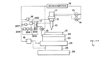
1 DESCRIPTION OF THE PREFERRED EMBODIMENTS
Fig. 1 is a view showing the structure of the
recording and reproducing apparatus of a first
embodiment according to the present invention. In
Fig. 1, a numeral 10 designates a probe electrode;
22, a substrate electrode; and 21, a recording medium
having the electric memory effect, which is sandwiched
between the probe electrode 10 and substrate electrode
22. The substrate electrode 22 and recording medium 21
are formed integrally on a substrate 23. A numeral
15 designates a voltage application means to apply a
voltage between the probe 10 and substrate electrode
22, and generate a voltage VB. A numeral 17 designates
a current detection means to detect a current flowing
between the probe electrode 10 and recording medium
21; 12, a Z-direction fine traveling control mechanism
to cause the probe electrode 10 to be traveled in the
Z direction finely; 16, a servo circuit to control the
distance (Z direction) between the probe electrode 10
and recording medium 21 using the Z-direction fine
traveling control mechanism 12 on the basis of the
current detection means 17. The servo circuit 16,
current detection means 17, and Z-direction fine
traveling mechanism 12 constitute a part of a space
controlling means to control the distance between the
probe 10 and recording medium 21. In the current
detection means 17, a numeral 201 designates a primary
l current-voltage converter having a sufficiently small
inner resistance 1 as compared with the resistance
between the probe electrode lO and substrate electrode
22, which outputs the detected current value after
having converted it into a sufficiently large voltage
signal corresponding thereto. Also, a numeral 202
designates a converter for converting the voltage
signal containing the signed (positive or negative
current (JT) received from the current-voltage
converter 201 to a signal corresponding to a
logarithmic value log ¦ JT ¦ of the absolute value of
the JT, and the output therefrom is transmitted to a
differential divider 203. The differential divider
203 outputs the difference between a signal 206 and a
signal corresponding to the log I JT ¦, the signal 206
corresponding to the logarithmic value of the
predetermined value of the tunnel current defined
so as to make the space between the probe electrode 10
and recording medium 21 a predetermined value. This
differential signal is transmitted to a frequency
filter 204 thereby to cut the high-frequency signal
corresponding to the recording information. A numeral
205 designates an amplifier circuit for amplifying a
signal which has passed through the filter 204. The
signal passed through the amplifier circuit 205 becomes
an information signal having an averaged space (averaged
space of an area sufficiently larger than the recording
- 10 -
1 bit) between the recording medium 21 and probe 10,
which is transmitted to a microcomputer 19. Then, on
the basis of this information signal, the microcomputer
19 transmits an instruction signal to the servo
circuit 16 so as to make the averaged space between
the probe electrode 10 and recording medium 21
constant.
Also, a part of the output of the converter
202 is directly transmitted to the microcomputer 19
through a frequency filter 207 which passes a high-
frequency signal and cuts a low frequency signal such
as corresponding to the averaged space information
between the probe electrode 10 and recording medium
21. At the time of information reproducing, this
signal becomes the recording information signal, which
is processed by the microcomputer 19 to reproduce.
A numeral 11 designates an x-y direction fine
traveling control mechanism for driving finely the
probe electrode 10 and fine traveling control
mechanism 12 in the x-y direction to cause the probe
electrode 10 to travel finely along the surface of the
recording medium 21. Numerals 13, 14 designate a y-
axial scanning driver and an x-axial scanning driver
for applying a y-direction driving control voltage Vy
and an x-direction driving control voltage Vx to the
x-y direction fine traveling control mechanism 11,
respectively. The x-y direction fine traveling control
1 mechanism 11 causes the probe electrode 10 to be
displaced in the x-y directions in accordance with the
voltage value applied respectively by the drivers 13
and 14. A numeral 24 designates an x-y stage to
enable the substrate 23 to travel in the X-Y directions
roughly; 25, a rough traveling mechanism to cause the
x-y stage 24 to travel in the Z direction roughly; 18,
a rough traveling driver to transmit controlling
signals to the x-y stage 24 and rough traveling
mechanism 25 in accordance with the instruction
signals from the microcomputer 19; and 26, a support
base.
Now, the operation of the recording and
reproducing in the structure set forth above will be
described.
Fig. 2A and Fig. 2B illustrate the changes per
time t in the x and y direction driving control
voltages Vx and Vy and the applied voltage VB by the
voltage application means 15 at the time of information
recording, i.e., the output states of the drivers 13
and 14 which have received instruction from the
microcomputer 19 and the means 15 as well as the
manner in which the recording is performed at that
time. The upper stage of Fig. 2A shows the waveforms
per time of the Y-axial driving control voltage Vy
applied to the x-y direction fine traveling control
mechanism 11 which causes the probe electrode 10 to
- 12 -
1 travel along the surface of the recording medium 21;
the middle stage thereof, the waveforms per time of
the driving control voltage Vx in the X axia~ direction
applied to the x-y fine traveling control mechanism 11;
and the lower stage thereof, the waveforms per time of
the voltage applied between the probe 10 and substrate
electrode 22. Fig. 2A is a time chart of the applied
voltage at the time of recording, and Fig. 2B is a view
schematically showing the manner in which information
is written onto the recording medium according to the
time chart shown in Fig. 2A as an example.
When the voltage Vx and voltage Vy are applied
as shown in the upper and middle stages of Fig. 2A,
the tip of the probe electrode 10 travels along arrows
sequentially over the positions represented by O on
the recording medium 21 as shown in Fig. 2B. The
traveling of the probe electrode 10 is substantially
instantaneous, and the probe electrode 10 stops at the
positions represented by O for a predetermined period
of time. In the lower stage of Fig. 2A, this
predetermined period of time is shown by numerals 31
to 40 per each position represented by mark O , and
also in each of the positions marked O , the position
at which a predetermined voltage is applied to generate
a change in the recording medium 21, is represented
by slanted lines in O in Fig. 2B. (This change, for
example, is a shift from the off-state to on-state in
13
1 a recording medium showing the memory switching
characteristics as disclosed in Japanese Patent Laid-
Open Application No. 63-161552). Further, the period
during which the voltage causing such change is applied
is represented by "on" in Fig. 2A, and all the other
periods, by "off". Hereinafter, in the other
embodiments which will be described later, the
representation is also made by "on" and "off" in the
same manner as in this case.
In the lower stage of Fig. 2A, the broken line
41 shows the upper potential level (zero level) of the
recording medium 21, and the broken line 42 shows the
threshold potential which causes the recording medium
21 at the phase level indicated by the broken line
41 to change (shifting to the on-state), respectively.
In the present embodiment, each of the recording bit
positions, i.e. in each of the periods 31 - 40, the
value of time integration rr VB (t) dt], of the applied
voltage VB (voltage between the medium 21 and probe
electrode 10) to the recording medium is substantially
zero. In other words, the averaged value of VB in each
of the periods becomes substantially zero. Specifically,
when there is no application of the voltage changing
the state of medium, which is represented by "off",
the absolute value of the applied voltage VB should be
equalized at half point in each of the periods to
inverse plus and minus. The absolute value of the
- 14 -
1 applied voltage VB at this time should be the value
suited for detecting the tunnel current JT in order to
control the average space between the probe electrode
10 and recording medium 21 constantly by the space
controlling means for controlling the distance between
the aforesaid probe electrode 21. This value should
be defined to be smaller than the threshold value to
generate a change in the medium 21 (to change the state
to be "on"), and if the absolute value is equal, there
is no substantial change in the output from the
converter 202 even when the sign of the applied
voltage VB changes. Thus, the aforesaid average
space control is performed during this period without
any substantial effect from such change in the sign of
lS the voltage VB. Also, when the voltage changing the
medium represented by "on" is applied, during the
period represented by "on" the state in which the
absolute value of the voltage VB is equal, should be
maintained in the most part of the period and the sign
of the voltage VB is inverted in the last short period
and the value of the voltage VB is made to exceed the
threshold value 42. At this juncture, the value of
the voltage should be adjusted to be [r VB (t) dt] - 0.
If a large value such as exceeding the threshold value
is applied, the value of the tunnel current JT is
increased during such period. However, since this
change is short enough, the aforesaid space controlling
- 15 - ~ ~
1 means does not substantially cause the probe electrode
10 to change its position in the Z direction practically
by this change in the value of the tunnel current JT.
In other words, at the time of the medium changing
voltage being applied, the aforesaid averaged space
control is executed continuously without receiving an
effect produced by the application of a large voltage.
As the above describes, irrespective of
whether the medium changing (shi~ting to the "on"
state) is generated or not, the charge once accumulated
by the voltage applied in one direction in a fine
region at which each of the recording positions is a
center is diffused by the voltage applied in the
opposite direction with making the value of time
integration of the applied voltage VB substantially
zero in each of the entire recording bit positions
(positions represented by O ), and this charged state
is eventually returned to the potential state before
the recording (removed electrically). Therefore, the
potential state over the entire recorded area of the
recording medium is not changed substantially. In
this respect, it may be possible to define the voltage
exceeding the threshold value, (i.e., the time at
which the voltage exceeding the threshold value is
applied during the period), at the start of each of
the periods not at the end thereof.
Particularly, as shown in the lower stage of
- 16 -
1 Fig. 2A, in the first embodiment the sections selected
by the means 11 to enable the probe electrode 10 to
travel along the surface of the recording medium 21,
have a point symmetry. In other words, during the
period represented by "off" the waveforms of the
applied voltage between the probe electrode 10 and
substrate electrode 22 in the fine region having each
of the recording bit positions as its center have
the point symmetry. By using the waveforms having
the point symmetry as the waveform of the applied
voltage corresponding to the periods represented by
"off", not only it is possible to perform [~ VB (t) dt]
~ 0 easily in this period, but by making the pulses
point symmetry, it is also possible to avoid and
extremely intensified voltage to be applied locally
in the region where no change is generated in the
recording medium.
Also, particularly, as shown in the lower stage
of Fig. 2A, in the first embodiment the sections
selected by the means 11 to enable the probe electrode
10 to travel along the surface of the recording medium
21 in the waveforms in the periods represented by "on",
have a point asymmetry. In other words, the waveforms
of the voltage applied between the probe electrode 10
and substrate electrode 22 in the fine region having
each of the recording bit positions as its center
have the point asymmetry to any points in the section.
- 17 -
1 By using the waveforms having the point
asymmetric property to any other points as the
waveforms of the applied voltage corresponding to the
periods represented by "on", it becomes easy to apply
an extremely intensified voltage locally under condition
of [I VB (t) dt] ~ 0 within this period; making it
possible to cause the medium change (shifting to the
"on" state) more reliably than conventional case.
As the recording medium 21, an organic thin
film having memory switching characteristics such as
disclosed in Japanese Patent Laid-Open Application No.
63-161552 is considered applicable.
Here, an example is considered for a recording
medium which shows the "on" state against an applied
voltage having the threshold value of approximately
three volts or more, while holding the "off" state
against an applied voltage of approximately three
volts or less without any change in its "on" state.
In the waveforms of the applied voltage
corresponding to the "on" state represented in the
periods 31, 33, 34, 36, and 39 in Fig. 2A, when,
for example, the applied voltage VB of possitive
polarity period 8QT (where QT is a 1/10 of the time
in one period) in the fore part of each period is
given as +lV and the applied voltage VB of negative
polarity period 2QT in the rear part is -4V, these
become 8QT x lV + 2QT x (-4) V = 0. Thus, an
1 8 -- Lf ~
1 application of voltage to the recording medium 21r
corresponding to the "on" state can be realized in
condition that the value of time integration of the
applied voltage in the fine region having each of the
recording bits as its center is zero.
Also, in the waveforms of the applied voltage
corresponding to the "off" state represented in the
periods 32, 35, 37, 38j and 40 in Fig. 2A, when, for
example, the applied voltage vB of possitive
polarity period 5QT in the fore part of each period
is given as +lV and the applied voltage VB of negative
polarity period 5~T in the rear part is -lV, these
become 5~T x lV + 5~T x (-1) V = 0. Thus, an
application of voltage to the recording medium 21,
corresponding to the "off" state (here, the application
of voltage by which the state of the medium is not
particularly allowed to be changed) can be realized
in condition that the value of time integration of the
applied voltage in the fine region having each of the
recording bits as its center is zero.
Subsequently, the information reproducing will
be described.
Fig. 3 is a view illustrating the changes per
time t of the driving control voltages Vx and Vy in the
x and y directions at the time of information
reproducing, and of the applied voltage VB by the
voltage application means 15. Fig. 3 is represented
-- 1 9 ~
1 by the same time chart as shown in Fig. 2A. Here,
the x-y direction driving of the x-y direction fine
traveling mechanism 11 portion including the probe
electrode 10 is the same as that of information
recording, so its description is omitted.
As in the case of the information recording,
the suspension periods of the probe electrode 10 are
designated by numerals 131 to 140. At each of the
recording bit positions also in information reproducing,
i.e., in each of the periods 131 to 140, the value of
time integration [I VB (t) dt] of the applied voltage
VB to the recording medium is substantially zero.
Specifically, at half point of each period, the
absolute value of the applied voltage VB should be
equalized to invert plus and minus. The absolute
value of the applied voltage VB at this time should be
the value suited for detecting the tunnel current JT
in order to control the averaged space between the
probe electrode 10 and recording medium 21 constantly
by the space controlling means therebetween and to
reproduce information. It is needless to mention that
this value is smaller than the threshold value which
generates changes in the medium 21. If the absolute
value is equal, the output from the converter 202 does
not practically changes even when the sign of the
applied voltage VB changes, and during this period,
the averaged space control and the reproducing of the
- 20 ~
1 recorded information are executed without receiving
any substantial effect from changes in the sign of
the applied voltage VB.
Nowr since the information reproducing
operation is repeatedly performed, the charge is
accumulated by the applied voltage, and it is more
liable to generate the molecular absorption on the
surface of the recording medium or the degradation or
deterioration of the film quality than that of the
information recording. Therefore, it is particularly
effective to make [r VB (t) dt] = 0 at each of the
recording bit positions.
Also, in consideration of the repeating
operation of the information reproducing, it is
lS particularly effective to avoid by the waveforms
having the point symmetry any extremely intensified
voltage which is locally applied.
Fig. 4 is a time chart showing the application
state of each of the voltages Vx, Vy~ and VB per time
t when the information recording is performed by a
recording and reproducing apparatus of a second
embodiment according to the present invention. The
structure of the apparatus is the same as shown in Fig.
1, and the application state of each of the voltages
Vx, Vy~ and VB per time t when the information
reproducing is performed, is the same as shown in Fig.
3. Further, the x-y direction driving of the probe
2 1 fd !~
1 electrode 10 is the same as described in conjunction
with Fig. 2. Therefore, its description of these
aspects are omitted.
The second embodiment is characterized in that
before or after or both before and after (in Fig. 4,
the case of only before is shown) the application of
a large voltage exceeding the aforesaid threshold value
during the "on" period represented in the lower stage
of Fig. 4, the pulse having the voltage with an inverted
sign, which is slightly larger than the voltage for
detecting the tunnel current JT, (but does not exceed
the threshold value) is once added. (Hereinafter,
this pulse voltage is referred to as "auxiliary pulse").
That is, the present embodiment is characterized
by having the auxiliary pulses (designated by numerals
61 to 66) whose absolute voltages are intensified in
the opposite polarity to written pulse before the pulse
portions 51 to S6 with the voltage exceeding the
threshold value (i.e. the written pulse), in the
waveforms during the period represented by "on" in
Fig. 4. Hence, it is possible to make the absolute
value of the written pulse voltage large with ease
under the condition of [~ VB (t) dt] = 0 in this
period, and to execute the medium change (shifting to
the "on" state) more reliably. The period of the
auxiliary pulse should be short enough so that the
change in the tunnel current JT upon the auxiliary
- 22 -
1 pulse application does not have an effect on the
control for making the averaged space between the probe
electrode 10 and recording medium 21 constant by said
space controlling means. However, in the case where
the probe electrode 10 tends to travel following the
changes in the tunnel current JT upon the application of
the written pulse or the auxiliary pulse (i.e. gain
being great) due to a slightly intensified feedback of
the space controlling means, the space between the probe
electrode 10 and recording medium 21 can be made larger
once prior to the application of the written pulse, by
adding this auxiliary pulses 61 to 66. If the space
is made large in advance as this case, the changes in
the tunnel current JT upon the written pulse application
can be made small, and an effect is obtainable to
prevent the space controlling means from becoming
unstable.
This second embodiment is also characterized
by having the pulse voltages (auxiliary pulses) with a
comparatively large point symmetry designated by
numerals 71 to 74 and 81 to 84 provided before and
after the boundary where the signs of the voltage VB
are changed, in the waveforms of the applied voltage
corresponding to the period represented by "off". In
the case where the space controlling means possesses a
slightly intensified feedback, it is possible by this
feature as in the period represented by "on" to change
- 23 -
1 the voltage polarities while keeping the probe electrode
10 slightly away from the surface of the recording
medium. There are some cases where depending on the
material of the recording medium, an adverse effect
such as the deterioration of quality thereof is observed
due to the rapid inverting of the polarity. However,
by inverting the polarity after the space has once
been made larger, the electric field in the recording
medium 21 is changed, whereby an effect is obtainable
to change the electric field in the recording medium
21 comparatively smoothly together with the nonlinearity
of the tunnel current.
Fig. S is a view showing a third embodiment
according to the present invention.
The third embodiment is the same as the first
embodiment with the exception of the aspects set forth
below. Therefore, the description is made only by the
same time chart as shown in Fig. 2A. The third
embodiment is characterized in that in the waveforms
of the applied voltage in the period represented by
"off", when the absolute value of the applied voltage
VB is equalized to invert plus and minus as in the
case of the first embodiment, there are provided a
plurality of periods with at least three or more periods
where the voltage VB is constant before and after this
inverting portion, and portions in which the level of
the relative voltage is gradually decreased or increased
24 ~
1 in the plurality of periods.
As the above describes, by changing the level
of the relative voltage gradually, it is possible to
change the signs of the voltage VB smoothly under
condition of [r VB (t) dt] 0 in this period, and to
prevent the space controlling means from becoming
unstable due to a rather large current to be generated
by the accumulated charge when the polarity of the
applied voltage is changed rapidly as well as the
quality of the recording medium from being deteriorated
due to the rapid change of the polarity.
In other words, the third embodiment has the
auxiliary pulse in the direction in which ¦ VB ¦ is made
small, before and after the boundary where the signs
of the voltage VB are changed in the waveforms in the
periods represented by "off". This auxiliary pulse is
effective when the feedback of the space controlling
means is weak (gain being small).
The third embodiment is also characterized by
having the auxiliary pulses (designated by numerals
101 to 106) whose absolute voltages are intensified in
the direction of the opposite polarity to the written
pulses after the written pulse portions 91 to 96, in
the waveforms of the applied voltage in the period
represented by "on". Thus, as in the case of the
auxiliary pulses of the second embodiment, it becomes
easy to make the absolute value of the pulse voltage
25 - ~d, ` ` ,,
1 large under the condition of [r VB (t) dt] _ 0 during
this period, and to perform the medium change (shifting
to the "on" state) more reliably.
Figs. 6A and 6B are views showing a fourth
embodiment according to the present invention. The
fourth embodiment is also the same as the first
embodiment with the exception of the aspects given
below. Therefore, the description will be made only
by the same time chart as in Fig. 3. The fourth
embodiment is recording and reproducing systems
characterized in that when the probe electrode 10 is
traveled along the surface of the recording medium 21
to scan a plurality of frames (one transversal row
designated by the reference mark O in Fig. 2B is
assumed to be one frame) at the time of information
recording and reproducing, applied voltages between the
probe electrode and the recording medium are defined so
that the integration average of the voltages
applied between the probe electrode and substrate
electrode in scanning the plurality of frames should
become substantially zero.
In particular, the fourth embodiment is
characterized in that performed is the recording and
reproducing of the information block which is the frame
scanning in which the probe electrode is scanned along
the surface of the recording medium in even-numbered
times, i.e., 2N-times (where N is a natural arbitrary
- 26 - ` ~`
1 number), and the absolute value of the applied voltage
between the probe electrode 10 and recording medium 21
is equalized at the time of one N-time frame scanning
and~the remaining N-time frame scanning in the frame
scanning of the even-numbered times (2N) to change the
voltage polarities (plus and minus) each other (this
changing being performed in the odd-numbered time and
even-numbered time, for example), whereby the value of
time integration of the applied voltage VB is made
substantially zero for the block as a whole.
Particularly, the present embodiment is
characterized in that the recording and reproducing
of the information block requiring a two-time frame
scanning are performed, and that the absolute values
of the applied voltages between the probe electrode
and recording medium in the two-time frame scanning
are equalized to change the voltage polarities each
other so as to make the value of time integration of
the applied voltage VB substantially zero in each of
the two frames.
Fig. 6A is a time chart at the time of
information reproducing and Fig. 6B is a time chart at
the time of information recording.
In Figs. 6A and 6B, a numeral 301 designates
the frame scanning period for a first time; 302, the
frame scanning period for a second time. Also, in Figs.
6A and 6B, reference marks Vy and Vx designate the
- 27 -
1 driving waveforms of the same means 11 to cause the
probe electrode to travel along the surface of the
recording medium as in Fig. 2A, and in the frame scanning
portion for the first time and the frame scanning portion
S for the second time, the probe electrode is arranged to
travel in the opposite directions while drawing the same
track on the recording medium. The manner of recording
and reproducing at this juncture, i.e., the way of
traveling of the probe electrode 10, are represented in
Fig. 6c using the same schematic view of Fig. 2s.
In Fig- 6A, the voltage VB is VB = + VBo (where
VBo is a constant) for the frame scanning period for
the first time, and VB = ~ VBo for the frame scanning
period for the second time.
In Fig. 6B, the voltage VB is defined to
provide its value of VB equivalent to a value suited
for detecting the tunnel current JT in the period
represented by "off" during the frame scanning period
301 in order to control the averaged space between the
probe electrode 10 and recording medium 21 constantly
by the space controlling means for controlling the
distance therebetween. This value should be smaller
than the threshold value generating a change (shifting
to the "on" state) in the medium 21.
Also, during the application period (represented
by ~on~) of the voltage changing the medium, the state
where the value of the voltage VB is equal to the one
- 28 - ~9;`~
1 during the period represented by "off" is maintained
in the most part of this period, and the value of the
voltage VB should be made to exceed the threshold only
in the last short period. Then, in the frame scanning
period 301 after the completion of the scanning for the
first time, the voltage application at each position
during the frame scanning period 301 is repeated at the
same position in the same manner while inverting the
polarities of the waveforms of the respective applied
voltages.
In the fourth embodiment, the accumulation of
the surface charge to the surface of the recording medium
is prevented by defining the applied voltage between
the probe electrode and recording medium to make the
integration average at each position substantially
zero in a plurality of frame scannings.
Also, in particular, it is possible to inspect
whether or not the data reading has been performed
correctly by executing the reading with a plurality of
frame scannings. For example, information for
detecting errors is provided in one information block,
and it may be possible to output the information which
has been read with the least error as a correctly
reproduced information among those plural readings
at the time of reproducing.
Likewise, by writing information onto the
recording medium for plural times (two times), a
- 29 -
1 recording and reproducing apparatus particularly
capable of avoiding writing failure can be implemented.
Now, in conjunction with Fig. 7 and Figs. 8A
to 8D, a fifth embodiment according to the present
invention will be described.
Fig. 7 is a view schematically showing the
structure of the fifth embodiment. The fifth embodiment
is an apparatus for recording, reproducing, and erasing
by the use of a plurality of probe electrodes having
means to enable them to travel along the surface of
the recording medium. In Fig. 7, reference numerals
401 and 402 designate the same electrode as the probe
electrode 10 shown in Fig. 1, respectively. The prove
electrode 401 is provided with a x-y direction fine
traveling control mechanism lla, z-direction fine
traveling control mechanism 12a, y-axial scanning
driver 13a, x-axial scanning driver 14a, voltage
application means 15a, servo circuit 16a, and current
detection means 17a as in the case of Fig. 1. The
operation of each constituent is substantially the
same as each of those described in the first embodiment.
The probe electrode 402 is also provided with
a x-y direction fine traveling control mechanism llb,
z-direction fine traveling control mechanism 12b, y-
axial scanning driver 13b, x-axial scanning driver 14b,
voltage application means 15b, servo circuit 16b, and
current detection means 17b as in the case of Fig. 1.
/ . ? ' : ~ ,?
- 30
1 The operation of each constituent is substantially
the same as each of those described in the first
embodiment. The probe electrodes 401 and 402 are set
apart by X0 (constant) from each other, and are
individually traveled in an area corresponding to a
certain block by the x-y direction fine travel driving
voltages Vxl, Vx2, and Vylr Vy2r respectively, while,
by a rough traveling driver 18, an x-y stage 24 is
driven to cause each of the probe electrodes to travel
evenly xO by xO to perform recording and reproducing.
The present embodiment is a recording and reproducing
apparatus wherein the integration average of the
voltages applied between the plural electrodes and the
substrate electrode at each bit on the recording medium
in a certain period is substantially zero.
In particular, the present embodiment is
characterized in that the recorded data in a certain
block in the recording medium is read by the use of a
pair of probe electrodes 401 and 402 which apply
voltages having the equal absolute values in each of
the blocks between the probe electrodes and substrate
electrode but opposite polarities to each other. This
pair of electrodes may be provided for a plurality of
the same pairs thereof.
In Fig. 7, the probe electrodes 401 and 402
are the probe electrodes which apply the voltages
VBl and VB2 having the equal absolute values between
- 31 -
~ ,, ~
1 the probe electrode and the substrate electrode, and
the opposite polarities to each other, by the voltage
application means l5a and 15b. In other words, for
example, the voltages applied at the time of
information reproducing are VBl = +VBo (~0), VB2 =
-VBo (<0) (where BBo > 0 is a real number).
__ _
- 32 ~
1 Fig. 8A is the same time chart as Fig. 2A
which shows each of the voltages applied to the two
probe electrodes 401 and 402 at the time of information
reproducing in one view.
Here, with the exception of the central
positions which are different, the probe electrodes
401 and 402 scan the recording medium in the same track
with the applied voltages having opposite polarities
but the same absolute values.
Fig. 8s is a view schematically showing the
positional relationship between each area of the
information blocks and each of the probe electrodes
at a certain time.
At the time represented by Fig. 8B, the probe
electrode 402 faces the block area 403 on the
recording medium while the probe electrode 401 faces
another block area 404 adjacent thereto on the
recording medium. Then, by applying bias voltages VBl,
and VB2 each having the opposite polarities but same
absolute values, the data in the block areas 403 and
404 are read with the probe electrodes which travel
along the positions designated by the mark O
sequentially as indicated by the arrow on each of the
block areas as in the case shown in Fig. 2B.
Fig. 8C is a schematic view the same as Fig.
8B and shows the state where the probe electrodes 401
and 402 have been traveled on the surface of the
- 33 - ~ ~ J `'
1 recording medium by the distance X0 in the same
direction by the x-y stage 24 driven by the rough
traveling driver 18 subsequent to the completion of
the reading at the state shown in Fig. 8B, and by
this shifting, the probe electrode 402 is caused to
face the block area 404 and the probe electrode 401,
another block area 405 adjacent thereto on the
recording medum. Then, Fig. 8C further illustrates
the probe electrodes reading the data in the block
areas 404 and 405 with the driving waveforms shown in
Fig. 8A as in the case of Fig. 8B.
With the operation set forth above, the block
area 404 is scanned in the same track by the bias
voltages having opposite polarities to each other
such as minus in the first stage and plus in the
second stage but the same absolute values. As a
result, the charge accumulated on the recording
medium 21 is offset. Then, the data reading in each
of the block areas is performed two times each by the
probe electrodes 401 and 402. In the respect, the
minus voltage is applied by the probe electrode 401
in the first stage to the block area 402, and the
plus voltage by the probe electrode 402 in the second
stage, for example.
Fig. 8D is a view showing each of t~le voltages
applied at the time of information recording with the
use of the same timing chart shown in Fig. 8A. The
- 34 -
1 value of voltage VB in the period represented by "off"
should be the value suited for detecting the tunnel
current JT to control the averaged space between each
of the probe electrodes and the recording medium 21
constantly by the space contro:Lling means to control
the distance therebetween. This value should be
smaller than the threshold value generating the
change (shifting to the "on" state) in the medium 21.
Also, during the period of applying the medium
changeing voltage, which is represented by "on", the
state in which the value of the voltage VB is the same
during the period represented by "off", should be
maintained in the most part of the period so that the
value of the voltage VB should exceed the threshold
value in the last short period.
Then, each of the probe electrodes 401 and
402 is driven relatively against the recording medium
21 as in the case of the information reproducing,
and when both probe electrodes scan the same block
area, the voltages having different waveforms are
applied only at the point where the polarities are
changed as VBl and VB2 shown in Fig. 8~. By repeating
this process for each of the block areas, the same
effect as in the information reproducing can be
obtained. Also, particularly, by writing information
plural times (two times) on the same block area, it
is possible to implement a recording and reproducing
- 35
1 apparatus capable of avoiding writing failure.
As the above describes, in the fifth embodiment,
a pair of probe electrodes having opposite polarities
but the equal absolute values are driven to travel
S X0 by X0 as mentioned above to scan the block areas
to reproduce information one after another, thus
making it possible to offset the accumulated changes
in the entire areas of the recording medium.
Also, by the use of a plurality of probe
electrodes to remove the charges electrically, it is
possible to write or read information onto or from
the recording medium plural times (two times) without
prolonging the reading or writing time, and to
implement effectively a recording and reproducing
apparatus capable of avoiding the possibility of
writing failure or reading error.
Fig. 9 is a view partially showing the
structure of a sixth embodiment according to the
present invention. With the exception of the aspects
set forth below, the structure of the present
embodiment is the same as the one shown in Fig. 1.
Accordingly, Fig. 9 illustrates only a part of its
structure.
The sixth embodiment is characterized in that
provided is a photo-conductive extrathin film layer
501 connected to the substrate electrode on the
recording medium 21 having the electric memory effect
36 ~
1 and grounded, and that after the recording and
reproducing is performed by the probc electrode 10
under the state that the photoconductivity layer 501
is made highly resistive, the photoconductive layer
501 is irradiated by light from a light source 502
to make it low resistive.
In Fig. 9, a numeral 504 designates a cover
shielding the system from the outside; and 503, the
grounding point of the photoconductive extrathin film
10 layer 501 and the substrate electrode 22. Although
the charge is accumulated in the recording medium
or on the surface thereof by the probe electrode 10
to perform recording and reproducing, it is possible
to discharge the accumulated charge in the recording
medium or on the surface thereof by making the
photoconductivity layer 501 low resistive with the
light irradiation from the light source 502 after
recording and reproducing as well as by the grounding
point to which the layer 501 is connected together
with the substrate electrode 22, thereby offsetting
the re ain;ng charge. In the present embodiment,
the recording and reproducing can be performed by
well known methods such as disclosed in Japanese Patent
Laid-Open Application No. 63-161552, Japanese Patent
Laid-Open Application No. 63-161553, and others.
Fig. 10 is a view showing a seventh embodiment
of the recording and reproducing apparatus according
- 37 - 2 `~
1 to the present invention.
With the exception of the aspects set forth
below, the structure of the seventh embodiment is also
the same as the one shown in Fig. 1. Accordingly,
Fig. 10 illustrates only a part of its structure.
The seventh embodiment is characterized by having a
grounding means connected to the substrate electrode
22 for the grounding and capable of arbitrarily
selecting the electrical non-connecting state or
connecting state against the recording medium.
In particular, a movable grounding plate
601, capable of traveling along the surface of the
recording medium and of contacting closely with an
arbitrary surface thereof, is used as the grounding
means. The movable grounding plate 601 is connected
to the substrate electrode 22 and is grounded as
designated by a numeral 602.
The seventh embodiment is such that after the
recording and reproducing by the probe electrode 10
using the well known method as in the sixth
embodiment, the movable grounding plate 601 is allowed
to be in contact with the surface of the recording
medium closely to discharge the accumulated charge on
the surface of the redording medium or in its inside.
Fig. 11 is a view showing an eighth embodiment
of the present invention.
With the exception of the aspects set forth
- 38 -
1 below, the structure of the present embodiment is
also the same as the one shown in Fig. 1. Accordingly,
Fig. 11 illustrates only a part of its structure.
The eighth embodiment is characterized in that the
charge deposited in the recording medium or on the
surface thereof is neutralized by spreading charged
particles over the surface of the recording medium.
In Fig. 11, numeral 701 designates a corona
discharging unit. In other words, in the eighth
embodiment, subsequent to the recording and reproducing
by the probe electrode 10 with the well known method
as in the first embodiment, the corona discharge with
an appropriate amount of the charged particles having
polarity offsetting the accumulated charge of the
applied voltage VB is performed by the use of the corona
discharging unit 701.
In the descriptions of the above-mentioned
embodiments, while an organic film having memory
switching characteristics is exemplified as the
recording medium 21, the present invention is not
limited thereto, and it may be possible to use a
medium which enables a gold thin film to generate
changes in shape as the medium having the electric
memory effect, for example. The present invention is
applicable to the case that the recording is made
onto such medium and the information reproducing is
performed by detecting the shapes recorded. In some
- 39 -
1 cases, even if a gold thin film is used, the charge
may also be accumulated on the extreme vicinity of
the surface, and if there is such problem, the present
invention can be expected to obtain the aforesaid
advantages.
The above-mentioned first through sixth
embodiments are particularly characterized in that
the driving voltage Vy in the axial direction Y has
the staged waveforms, and the driving voltage Vx in
the axial direction X has the staged waveforms of
different frequency in synchronism with Vy~ and the
average of applied voltages is zero in the period
during which the application state of (Vx, Vy) is
selected in condition that the waveforms of the
voltages applied to the recording medium are in
synchronism with Vx and Vyr i.e., the suspension
period at the positions designated by the mark O.
However, the present invention is not limited thereto.
For example, it may be possible to make the
driving voltage Vy in the axial direction Y, a
voltage waveform of trigonometrical waveform, and
the driving voltage Vx in the axial direction X, a
voltage waveform of trigonometrical waveform of
different frequency in synchronism with Vy~ Even with
this arrangement, it is possible to make the average
of the applied voltages zero in the period during
which the traveling probe electrode scans the area
- 40 ~
1 Of one bit to plural bits portions in a state where
the waveforms of voltages applied to the recording
medium are in synchronism with Vx and Vy~
Also, while the above-mentioned embodiments
are recording and reproducing appara~us, the present
invention may also be applicable to an apparatus which
performs only recording or reproducing.
Also, the present invention can suitably be
used for the STM system and its application equipment
employed as an information reading apparatus.
With each of the embodiments set forth above,
it becomes possible to perform a highly precise
information reading or inputting at all times without
producing any adverse effects on the information
medium due to the charge accumulation caused by the
applied voltage.