Note: Descriptions are shown in the official language in which they were submitted.
APPARATUS FOR MAINTAINING COHERENCY~ ~ 8 4 7 3
OF CACHE MEMORY DATA
BRIEF DESCRIPTION OF THE DRAWINGS
Fig. 1 is a structural diagram of a system
explaining an operation for maintaining coherency of memory
data in a conventional data processor having a cache memory.
Fig. 2 is a logic diagram for passive invalidation
processing in a data processor structured as shown in
Fig. 1.
Fig. 3 is a structural diagram of a system
explaining an operation for maintaining coherency of memory
data in another conventional data processor having a cache
memory.
Fig. 4 is a logical diagram for active
(intentional) invalidation processing in a data processor
structured as shown in Fig. 3.
Fig. 5 is a structural diagram of a system
explaining an operation for reserving coherency of memory
data in a conventional data processor according to an
embodiment of the present invention.
Fig. 6 is a logic diagram for executing
invalidation processing of a store-through type cache memory
in the data processor shown in Fig. 5.
BACKGROUND OF THE INVENTION
1. Field of the Invention
The present invention relates to a data processor
having a cache memory, and particularly to a system for
reserving coherency of data stored in main memory and data
stored in the cache memory.
2. Prior Art
Fig. 1 is a system structure diagram for
explaining an operation for maintaining coherency of memory
data in a conventional data processor having a cache memory.
In this figure, system I comprises a first processor 100
which executes data processing, a main memory 101 and a
second processor 102 which executes data processing sharing
7 3
--2--
the main memory 101 with the first processor 100. The
processor 100 comprises a cache memory 103 which stores a
copy of the contents of the main memory 101 by maintaining
the contents with the store-through method for data
processing. The first processor 100 and the main memory 101
are connected with a first memory bus 104a, while the second
processor 102 and the main memory 101 are connected with a
second memory bus 104b. When the processor 102 operates to
cause its contents to be stored in the main memory 101, a
cache invalidation request signal 105 for requesting
invalidation of cache memory 103 is transmitted and
completion of the cache invalidating operation by the first
processor 100 is notified by a cache invalidation completion
signal 106.
Fig.2 is a logical diagram showing passive
invalidation of a store-through cache in a conventional data
processor. In this figure, a data processor comprises a
cache memory controller 1 which includes a data array in the
cache memory 103 and processes a cache memory access from
the first processor 100 and a cache memory invalidation
request; a tag memory 2 which comprises an address part and
a validity indicating part which indicates that memory data
corresponding to the address part exists in the cache
memory, in order to control, for each cache block,
registration of memory data held in the data array within
the cache memory controller 1; an invalidation input
register 3 which receives a cache invalidation request
signal 105 when the second processor 102 requests the main
memory 101 to store data; an invalidation address register 4
which receives a cache memory invalidation request address
from the first memory bus 104a simultaneously with reception
of the cache invalidation request signal 105 by the
invalidation input register 3; and an invalidation address
comparator 5 which compares the contents of the address part
read from the tag memory 2 with the contents of the
invalidation address register 4 excluding the address part
in the cache block and the address part used for reading the
~847~
--3--
tag memory 2, so as to detect coincidence
between those contents. The reference numerals 6, 10, 12
denote AND gates; 9, a NAND gate; 7, 11, OR gates and 8, an
invalidation request register for sending an invalidation
request to the cache memory controller 1 on the basis of the
fact that the cache memory invalidation request address held
in the invalidation address register 4 exits in the cache
memory 103.
Fig. 3 is a structural diagram of a system for
explaining operations for maintaining coherency of memory
data in a cache memory of another conventional data
processor. In this figure, a system II comprises a first
processor 200, a main memory 201, a second processor 102 and
a cache memory 103. The first processor 200 and the second
processor 102 are connected through a common memory bus 104
for the purpose of getting access to the main memory 201.
Fig. 4 is a logical diagram for actively, namely, positively
executing invalidation of the store-through type cache
memory 103 within the first processor 200 of the system
structure shown in Fig. 3. In Fig. 4, the first
processor 200 comprises a cache memory controller 1, a tag
memory 2, an invalidation input register 3, an invalidation
address register 4, an invalidation address comparator 5,
AND gates 6, 12, 21, an OR gate 7 and an invalidation
request register 8 and is connected as shown in the figure.
Next, an operation for maintaining coherency of
memory data in the data processor of the system I will be
explained with reference to Fig. 1 and Fig. 2. When the
second processor 102 sends a data storing request through
the second memory bus 104b to the main memory 101, the main
memory 101 updates the contents in accordance with the
storing request. If, at the time of the update of data, a
copy of the main memory 101 including old memory data to be
updated are stored in the cache memory 103 in the first
processor 100, it is required to maintain coherency
(consistency) of data so that the first processor 100 should
not use data not renewed after data has been updated. For
-4- ~ ~ ~8~3
this purpose, the main memory 101 sends a cache invalidation
request address and a cache invalidation request signal 105
via the first memory bus 104a to the first processor 100 so
that a copy of memory data in the cache memory 103
corresponding to the store request issued by the second
processor 102 is invalidated. In the first processor 100,
the cache invalidation request address is received by the
invalidation address register 4 through the first memory
bus 104a, while the cache invalidation request signal 105 is
received by the invalidation input register 3, respectively.
Next, with the output of the invalidation address
register 4, the tag memory 2 is accessed to read out the
address part and validity indicating part which indicate the
situation of registration with regard to a relevant cache
block. The address part read from the tag memory 2 is
input to the invalidation address comparator 5 and is
compared with the content of the invalidation address
register 4 excluding the address part to be used to read the
tag memory 2 and the address part within the cache block.
When the address part coincides with the address part in the
invalidation address register as a result of the comparison
explained above, the invalidation address 5 outputs a
logical 1, and, when these do not coincide, the comparator 5
outputs a logical 0. The validity indicating part indicates
whether the data of the cache block corresponding to the
invalidation address register 4 and read from the tag
memory 2 has been registered validity, and becomes a
logical 1 when the data has been registered and a logical 0
when not registered. When three conditions, (1) the
invalidation input register 3 outputs a logical 1, namely,
the cache invalidation request exists; (2) the output of the
invalidation address comparator is a logical 1, namely, the
invalidation address coincides with the memory address held
by the cache block in the cache memory 103; and (3) a value
of the validity indicating part read from the tag memory 2
is a logical l, namely, the cache memory 103 holds a copy of
the main memory 101, are established, the AND gate 6 opens
7 ~'~ 8 ~ 7 ~
--5--
and outputs a logical 1 and thereafter the OR gate 7 opens
and outputs a logical 1, thereby putting the invalidation
request register 8 in a set condition. On the other hand,
when the AND gate 6 opens, the output of NAND gate 9 becomes
a logical 0, closing the AND gate 10. Therefore, the OR
gate 11 which generates the cache invalidation completion
signal 106 does not open. If a copy does not exist in the
cache memory 103 when the invalidation input register 3 is
in a set condition, namely, when the invalidation address
comparator 5 outputs a logical 0 due to no coincidence or
when the validity indicating part read from the tag memory 2
is in a logical 0 state which indicates no data has been
registered, the AND gate 6 does not open and the signal
which places the invalidation request register 8 in a set
condition through the OR gate 7 is not generated.
On the other hand, since the NAND gate 9 opens and
outputs a logical 1, the AND gate 10 opens and outputs the
cache invalidation completion signal 106 through the OR
gate 11.
Subsequently, the request for invalidating the
data in the cache memory 103 set by the invalidation request
register 8 and the cache invalidating address held in the
invalidation address register 4 are input to the cache
memory controller 1. Upon reception of the request from the
invalidation request register 8, the cache memory
controller 1 determines priority between access requests to
the cache memory 103, accepts the request by the
invalidation request register 8 when there is not any other
request having higher priority than the cache memory
invalidating request, writes the tag memory 2 to put the
validity indicating part to a logical 0 state, that is, a
non-registered state using the content of the invalidation
address register 4, and outputs an invalidation completion
message. With the invalidating completion message output
from the cache memory controller 1, the OR gate 11 opens and
outputs the cache invalidation completion signal 106.
Moreover, with the invalidation completion message, the AND
~ ~ 4 8 ~ 7 ~
--6--
gate 12 is closed and outputs a logical 0, thereby clearing
the invalidation request register 8.
The main memory 101 which has received the cache
invalidation completion signal 106 terminates the processing
of writing the store requested data from the processor 102
at a relevant address.
When the second processor 102 reads data from the
main memory 101 through the second memory bus 104b, the
cache invalidation request signal 105 sent to the first
processor 100 is not asserted. Therefore, no cache
invalidating operation is initiated in the first
processor 100. This operation is common in the following
operation and therefore an explanation thereof will be
omitted.
Next, with reference to Fig. 3 and Fig. 4 an
operation for maintaining coherency of memory data in the
data processor of the system II will be explained. The
second processor 102 puts a store request on the common
memory bus 104 and sends the request to the main memory 201.
At the same time, the processor 102 drives a logical 1
indicating to store data by a W/R# signal representing a
data transfer direction, that is, whether data is to be
stored or fetched, the W/R# signal existing on the common
memory bus 104. Next, memory address information in the
store request is placed in the common memory bus 104 and the
second processor 102 asserts an address strobe signal in
order to transfer the memory address information to the main
memory 201. When this address strobe signal is asserted,
the main memory 201 receives the information in the common
memory bus 104 as a store address. At this time, since the
W/R# signal is a logical 1, the address strobe signal is
asserted in a logical 1 state, and the cache memory
controller 1 outputs a logical 0 indicating that the
controller is not using the common memory bus 104, the AND
gate 21 opens and outputs a logical 1. The logical 1 output
from the AND gate 21 is set in the invalidation input
register 3 and causes the store address from the second
processor 102 on the common memory bus 104 to be sampled and
7 ~ ~ ~ 8 4 7 ~
stored in the invalidation address register 4.
Subsequently, the invalidation address
comparator 5 and the AND gate 6 decide, by reading the tag
memory 2, if a corresponding copy of data of the main
memory 201 at the address sampled in the invalidation
address register 4 is stored in the cache memory 103, and,
when the copy exists in the cache memory 103, the cache
memory controller 1 executes an invalidating operation.
These operations are the same as those performed in the
system I and therefore an explanation of such operations is
omitted here.
It is noted that the only difference between
Fig. 4 and Fig. 2 is that cache invalidation completion is
not notified to the main memory 201. That is, when the
store request of the second processor 102 passes through the
common memory bus 104, the first processor 200 can terminate
the cache invalidating operation by monitoring
traffics of the bus 104, and accordingly the invalidating
operation completion need not be notified.
Since conventional data processors are structured
such as explained above, if a system structure is different,
an operation for maintaining coherency of a cache memory
also becomes different. Therefore, different logical
structures must be employed, which prevents common use of a
processor and forces a new development of processors for
each system structure. These changes in system structures
have been insufficient. Moreover, in the case where a
system structure having a double layered cache is employed,
all traffics of a common memory bus must be transferred to a
processor bus, resulting in a danger of lowering the
performance of a system.
SUMMARY OF THE INVENTION
The present invention has been proposed to solve
the problems explained above and it is therefore an object
of the present invention to provide a data processor which
flexibly deals with any change in a system structure for the
~ ~8473
--8--
purpose of maintaining coherency of memory data in a data
processor comprising a cache memory, and suppresses any slow
down in system performance by means of a coherency
maintenance operation.
In view of achieving this object, a data processor
according to the present invention comprises a main
memory, a main processor including a cache memory and a
plurality of subprocessors all interconnected through a bus,
and, when any one of the subprocessors have stored data at a
predetermined address in the main memory, operates to
invalidate the data stored at the address of the cache
memory corresponding to the predetermined address so as to
maintain coherency of data of the cache memory.
The main processor comprises, in order to maintain
coherency of data stored in the cache memory, (1) a first
means for detecting that any one of the subprocessors have
stored data to the main memory to actively monitor whether
valid data is held or not at the cache memory corresponding
to the address of the stored data so as to invalidate the
stored data when valid data is held, (2) a second means for
receiving a cache invalidating signal when any one of the
subprocessors have stored data in the main memory to obtain
the stored data and for passively monitoring whether valid
data is being held or not at the cache memory corresponding
to the obtained address so as to invalidate the held data
when valid data is held, and (3) a third means for
selectively operating the first means, second means or both.
In view of achieving the object of the present
invention, a data processor according to the present
invention may also comprise a cache memory control system, a
main processor, a cache memory, a main memory and a
plurality of subprocessors all interconnected through a bus,
and, when any one of the subprocessors have stored data at a
predetermined address in the main memory or the cache
memory, operates to invalidate the data stored at the
address of the cache memory corresponding to the
predetermined address so as to maintain coherency of data of
. ,i
~ ~ ~ 8 4 7 ~
_9_
the cache memory.
The cache memory control system comprises, in
order to maintain coherency of data stored in the cache
memory, (1) a means for storing an operation mode, said
operation mode corresponding to the particular system
structure of the data processor, (2) a first means for
detecting that any one of the subprocessors have updated
data in the cache memory to actively monitor whether valid
data is held or not at the cache memory corresponding to the
address of the updated data so as to invalidate the cache
memory data when the data is updated, (3) a second means for
receiving a cache invalidating signal when any one of the
subprocessors have stored data in the main memory, to
receive the address of the stored data, and for passively
monitoring whether valid data is being held or not at the
cache memory corresponding to the received address so as to
invalidate the held data when valid data is held, and (3) a
third means for selectively operating the first means,
second means or both, based on the operation mode.
A data processor in the present invention is
capable of realizing a variety of system structures using
one type of data processor (for example, formed by a single
LSI) and also enhancing utility of a data processor because
an operation for reserving coherency can be changed only by
setting an operation mode selected out of several operation
modes for maintaining coherency of memory data by a
selecting means without changing the system logic.
Moreover, any drop of system performance can be minimized
because an optimum operation mode for maintaining coherency
can be selected.
DETAILED DESCRIPTION OF THE PREFERRED EMBODIMENTS
A preferred embodiment of the present invention
will be explained with reference to the accompanying
drawings.
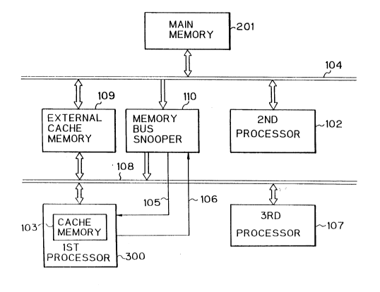
Fig. 5 is a structural diagram of a system for
explaining an operation for maintaining coherency of memory
4 ~ ~
--10--
data in a data processor having a cache memory, according to
the present invention. In this figure, elements similar to
those in Fig. 1 and Fig. 3 are designated by the same
reference numerals and explanations about these elements
will be omitted here.
A data processor of the present invention further
comprises a third processor 107 which executes data
processing using the main memory 201 in common with the
first processor 300 and the second processor 102; a
processor bus 108 which is used to pass memory address and
data when the first processor 300 and third processor 107
make access to the main memory 201 and to transmit memory
address information when the cache memory 103 is requested
to be invalidated; a store-through type external cache
memory 109 which is used by the first processor 300 and the
third processor 107 to store a copy of the main memory 201;
and a memory bus snooper 110 which monitors access from the
second processor 102 to the main memory 201 via the common
bus 104 and transmits, when a store request is generated, a
cache invalidation request signal 105 and an invalidation
request address to the first processor 300 through the
processor bus 108.
Fig. 6 is a logical diagram for invalidating the
store-through type cache memory 103 in the data processor
according to the present invention. In this figure, the
elements similar to those indicated in Fig. 2 and Fig. 4 are
denoted by the same reference numerals and these elements
will not be explained here.
The first processor 300 further comprises a
coherency operation mode flag (hereinafter referred to as
"flag") 20 for controlling an operation mode to maintain
coherency of memory data in the cache memory 103; a
selector 23 for selecting a kind of invalidation request
input to the cache memory 103 based on the content of the
flag 20; a cache invalidation completion input control
register 24 for controlling a cache invalidation completion
signal 106; and an invalidation completion control
i~ ~ 4 ~ 4 ~ ~
--11--
register 27 for controlling the cache memory controller 1 to
cause a cache invalidation completion signal 106 to be
output when the cache memory 103 is to be invalidated on the
basis of the content of the cache invalidation completion
input control register 24.
Next, the operation of this embodiment will be
explained. A logical structure within the processor 100
shown in Fig. 6 are applicable, depending on the content of
flag 20, not only to the system structure of Fig. 5 but also
to the system structure of Fig. 1 and to the system
structure of Fig. 3.
(1) Operation in the system structure I of Fiq. 1
In this case, the operation is similar to the
operation explained with reference to Fig. 1 and Fig. 2 and
therefore only a difference from the prior art will be
explained. Here, the memory bus 108 shown in Fig. 6
corresponds to the first system bus 104a in Fig. 1.
Prior to commencement of the system operation, an
operation mode corresponding to the system structure of
Fig. 1 is set in the flag 20. The preset content enables
selection of a cache invalidation request signal 105 as the
output of selector 23 and has such a value as to cause the
cache invalidation request signal 105 to be input to the
cache invalidation completion input control register 24.
After the commencement of the system operation
under this condition, when the second processor 102
transmits a store request to the main memory 101 through the
second memory bus 104b, the main memory 101 updates stored
data in response to the store request. With the update of
data, the main memory 101 sends a cache memory invalidation
request address to the main processor 100 through the first
memory bus 104a and drives the cache invalidation request
signal 105 to a logical 1. In the first processor 100, the
cache invalidation request signal 105 is sent to the
invalidation input register 3 and cache invalidation
completion input control register 24 through the
-12- ~ 4 ~ ~
selector 23. Simultaneously, the invalidation request
address in the first memory bus 104a is sent to the
invalidation address register 4. Thereafter, as explained
above, it is decided using the tag memory 2, invalidation
address comparator 5 and AND gate 6 whether a copy of data
of the main memory 101 at the address sampled to the
invalidation address register 4 is being held in the cache
memory 103 or not. If such a copy exists in the cache
memory 103, the invalidation request register 8 is set, and
thus the cache memory controller 1 executes such an
invalidating operation as explained previously. If it is
proved that a copy of data does not exist in the cache
memory as a result of decision made by reading the tag
memory 2 when the invalidation input register 3 is set, the
AND gate 9 opens. At this time, since a cache invalidation
input control register 24 is set with the cache invalidation
request signal 105 and outputs a logical 1 under the
control of the flag 20, the AND gate 10a opens and outputs a
logical 1. As a result, the cache invalidation completion
signal 106 is output through the OR gate 11 and the
completion of invalidation processing is informed to the
main memory 101.
When a copy of memory data to be invalidated
exists in the cache memory 103, the completion of
invalidation is reported such as explained hereunder. When
the output of the logic gate 6 is set to a logical 1, the
invalidation request register 8 is set to a logical 1
through the OR gate 7. Simultaneously, since the cache
invalidation completion input control register 24 is set to
a logical 1, the AND gate 25 opens and outputs a logical 1
whereby a logical 1 is set in the invalidation completion
control register 27 through the OR gate 26. The
invalidation completion control register 27 set to 1 is kept
at the level of logical 1 by the AND gate 28 and the OR
gate 26 until the cache memory controller 1 completes
invalidation of the cache memory 103.
The cache memory controller 1, receiving an
~4~47~
-13-
invalidation request from the invalidation request
register 8, outputs a logical 1 to execute invalidation
processing and opens the AND gate 29. Accordingly, a cache
invalidation completion signal 106 is output to the main
memory 101 through the OR gate 11. Simultaneously, the AND
gates 12, 28 are closed thereby clearing the invalidation
request register 8 and the invalidation completion control
register 27.
(2) Operation in the system structure II shown in Fig. 3
Among the operation of this case, what was already
explained with reference to Fig. 3 and Fig. 4 and the
operation already explained in the paragraph 1 as a part of
the operation of the present invention are not explained
here for simplicity. The memory bus 104 in Fig. 3
corresponds to the memory bus 108 in Fig. 6.
Prior to the start of system operation, an
operation mode corresponding to the system structure of
Fig. 3 is set in the flag 20. This preset content has a
value to select the output of the AND gate 21 as the output
of the selector 23 and control the cache invalidation
completion input control register 24 so that the main
memory 201 does not receive the cache invalidation request
signal 106. As explained above, when the flag 20 is set, a
logical 0 is always set in the cache invalidation completion
input control register 24, whereby, the AND gate 25 is
closed and the invalidation completion control register 27
is set to a logical 0 through the OR gate 26. Since the
cache invalidation completion input control register 24 is
set to a logical 0, the AND gate 10a is closed and outputs a
logical o. Moreover, since the invalidation completion
control register 27 is set to a logical 0, the AND gate 29
is closed and outputs a logical 0. Accordingly, the cache
invalidation completion signal 106 output through the OR
gate 11 remains set at a logical 0.
After the flag 20 has been set, a system operation
starts. The second processor 102 places a store request
2~ 4~4~
-14-
address to the main memory 201 in the common memory bus 104
and sets the W/R# signal to a logical 1. Next, the second
processor 102 drives an address strobe signal to a logical 1
in order to sample the store request to the main memory 201.
In this case, the main memory 201 receives the store request
address and W/R# signal from the memory bus 104 and starts a
storing operation. Simultaneously, in the first
processor 100, the AND gate 21 opens and outputs a
logical 1. This output is selected by the selector 23
depending on the value set in the flag 20, whereby a
logical 1 is set in the invalidation input register 3 and an
invalidation request address is set in the invalidation
address register 4. Thereafter, as explained previously, it
is decided whether a copy of memory data corresponding to
the invalidation request address has been registered to the
cache memory 103 or not. When the copy has been registered,
the registered data is invalidated. However, as explained
above, the only difference is that the flag 20 is set so as
to drive a cache invalidation completion signal 106.
(3) Operation in the sYstem structure of Fiq. 5
Prior to the start of a system operation, an
operation mode corresponding to the system structure of
Fig. 5 is set in the flag 20. This preset content has a
25 value to select the output of the OR gate 22 as the output
of the selector 23 and input a cache invalidation request
signal 105 to the cache invalidation completion input
control register 24.
After a system operation is started under this
30 condition, the following operations are executed for the
purpose of maintaining coherency of the cache memory 103 in
the first processor 300.
3-1 Operation when the second processor 102
makes an access to the main memorY 201
In the case the second processor 102 has issued a
store request through the common memory bus 104 to the
main memory 201, the external cache memory 109 and the
~ ~ ~ % 4 ~ 3
-15-
memory bus snooper 110 simultaneously monitor independently
the existence of a store request on the memory bus 104, and,
when the external cache memory 109 holds therein a copy of
the data of the main memory 201, the external memory 109
invalidates such copy. Meanwhile, the memory bus
snooper 110 transmits an interruption to the processor bus
108 and outputs a memory address corresponding to the store
request sent from the second processor 102 to the processor
bus 108 as a cache invalidation request address and sets a
cache invalidation request signal 105 to a logical 1. In
the first processor 300, since the cache invalidation
request signal 105 is a logical 1, the OR gate 22 opens and
outputs a logical 1. This output is selected by the
selector 23 depending on the value preset in the flag 20 in
accordance with the operation mode to set the invalidation
input register 3, and the invalidation address register 4
receives a cache invalidation request address from the
processor bus 108. Moreover, the cache invalidation request
signal 105 is input to the cache invalidation completion
input control register 24 to set it to a logical 1 under the
control of the value preset in the flag 20. Thereafter, as
was already explained in the paragraph (1), the cache
memory 103 is invalidated and the cache invalidation
completion signal 106 is output.
3-2 Operation executed when the third
processor 107 accesses the main memory 201
When the third processor 107 outputs a store
request to the external cache memory 109 through the
processor bus 108 for the purpose of making access to the
main memory 201, the first processor 300 opens the AND
gate 21 in accordance with the same operation as that
explained in the paragraph (2). The output of the OR
gate 22 sets the invalidation input register 3 through the
selector 23, and the invalidation address register 4
receives a store address as a cache invalidation request
address. The subsequent operations are the same as those
explained in paragraph (2). A cache invalidation completion
-16-
signal 106 is not output, because the cache invalidation
request signal 105 is not asserted in this case.
The operations explained in paragraphs 3-1 and 3-2
are serialized and do not compete with each other in the
main processor 300 because the right to use the processor
bus 108 is exclusively taken. Therefore, even in such a
system structure as shown in Fig. 1, coherency of memory
data can be correctly reserved.
In the above embodiment, a store-through cache has
been employed for the cache memory 103 in the main processor
300 and the external cache memory 109 for simplifying the
explanation, but even in the case the store-in cache is
employed, a similar advantage as that of this embodiment can
be obtained.
Moreover, a data processor using a cache memory is
disclosed in Japanese Patent Public Disclosure
No. 233537/lg89, but this processor is intended to provide
means for selectively setting/resetting an operation
corresponding to any one of application purposes (for data
and for instruction) of a cache memory, and is different in
operation and advantage from the apparatus disclosed in the
present invention in that a plurality of modes of operation
for maintaining a match between a copy of memory data
(regardless of data and instruction) in the cache memory and
memory data within the main memory, that is, an invalidation
of a buffer of maintenance of data coherency, and for
designating/cancelling an operation more selectively or in
combination.
Japanese Patent public Disclosure No. 21783/1984
also discloses an apparatus which is intended to enhance
utility of system by enabling a change in structure of a
memory system by providing means for setting/resetting a
processing mode of memory storing operation (store) in a
store-in type cache memory which is used in common by a
plurality of access request apparatus (for example, CPU),
but such a disclosed apparatus is different from the present
invention in object, construction and advantages.