Note: Descriptions are shown in the official language in which they were submitted.
CA 02048564 2001-04-12
OPTICALLY VARIABLE INTERFERENCE DEVICE
WITH PEAK SUPPRESSION AND METHOD
This invention relates to an optically variable
interference device having peak suppression and a
method.
In U.S. Patent Nos. 4,705,300; 4,705,355 and 4,779,898
there are disclosed thin film optically variable
articles and a method for which provides a limited range
of optically shifting colors in the interference
designs. These colors are based on an interference
phenomenon which resulted by tilting the thin film
coating to change the effective light interference path.
These designs in combination with blocking dyes have
made it possible to achieve additional colors by
subtracting a col.o:r ar modifying a color or blocking
colors at high angles. Such approaches, however,
provide only a limited range of optically shifting
colors. There is a need for additional colors which can
be utilized in optically variable interference devices
or optical shifter~~ of a thin film design.
CA 02048564 2001-04-12
-2-
In general it is an object of the present invention to
provide an optica:Lly variable interference device and
a method in which additional colors can be provided.
Another object of t:he invention is to provide a device
and method of the above character in which peak
suppression is utilized.
Another object of t:he invention is to provide a device
and method of the above character in which two or more
periods are utilized.
Another object of the invention is to provide a device
and method of the above character in which at least one
color is suppressed'..
Another object of the invention is to provide a device
and method of the above character in which multiple
colors are suppres~~ed.
Another object of the invention is to provide a device
and method of the above character which provides a
higher color saturation and purity.
Another object of the invention is to provide a device
and method of the above character in which a wide
suppression range i.s utilized.
Another object of the invention is to provide a device
and method of the above character in which there is
suppression in the infrared.
CA 02048564 2001-04-12
-3-
Additional objects and features of the invention will
appear from the fol:Lowing description of the preferred
embodiments as set forth in detail in conjunction with
the accompanying drawings.
FIG. 1 is a cross-sectional view showing an asymmetric
design of an optically variable interference device with
periodic peak suppression incorporating the present
invention.
FIG. 2 is a cross-;sectional view showing a symmetric
design of an optically variable interference device with
periodic peak suppression incorporating the present
invention.
FIG. 3 is a graph showing a red to green optical
variable interference device.
FIG. 4 is a graph showing a comparison from red to green
and magenta to green optically variable interference
device.
FIG. 5 i.s a graph similar to FIG. 3 but showing the
reflectance by wave number rather than by wave length.
FIG. 6 is a graph showing a blue to black optically
variable interference device.
FIG. 7 is a graph showing a gray to red optically
variable interference device.
FIG. 8 is a graph showing a prior art green to blue
optically variable interference device.
CA 02048564 2001-04-12
-4-
FIG. 9 is a graph showing a blue to green optically
variable interference device with suppression.
FIG. 10 is a graph showing curves for single, two, three
and four period designs.
In general, the optically variably interference device
having peak suppre:~sion is comprised of a substrate
having first and second surfaces. A thin film
multilayer interference coating is disposed on the first
surface . The interference coating is comprised of a
metal reflector layer having a surface and at least two
periods formed on t:he surface of the metal reflector
layer with each period being comprised of a metal
absorber layer and a spacer dielectric layer. The
reflector interacts with the at least two periods of the
interference coating to cause peak suppression at a1:1
angles in the design due to inteference effects in the
design by itself of at least two periods.
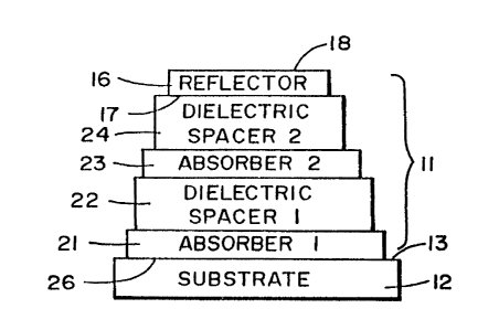
As more particularly shown in FIG. 1 of the drawings,
the optically variable interference device 11 of the
present invention is disposed on a substrate 12. The
substrate 12 can be :Formed of any suitable material such
as a flexible web, formed of a suitable plastic such as
PET and of a suitable thickness as for example ranging
from two to seven. mils. The optical variable
interference of device 11 is in the form of a multilayer
thin film stack which is comprised of a reflector layer
16 having surfaces :17 and 18 with at least two periods
being disposed on c>ne of the surfaces as for example
surface 17 to provide an asymmetric device . Each of the
periods is formed of a metal absorber layer and a spacer
CA 02048564 2001-04-12
-5-
dielectric layer. In order to form the thin film
interference stack 11 on the substrate to provide the
asymmetric optical. variable interference device 11, the
thin film layers forming the periods are deposited in
reverse order upon the surface 13 of the substrate 12.
Thus absarber layer 1 is first deposited on the surface
13 of the substrate 12 and is followed by a dielectric
spatial .Layer 1 identified as 22 to provide the first
period and this is followed by an absorber layer 2
identified as layer 23 and a dielectric spacer layer 2
identified as 24 for the second period, after which
there is deposited thereon the reflector layer 16.
Thus, it can be seen that a two period interference
stack is provided with two dielectric spacers and two
absorbers in alternating order.
It has been found to achieve the best color in a two
period multilayer interference stack, the outer absorber
layer 1 should be between one third and one half the
thickness of the innermost absorber layer. For best
results it has been found that absorber layers should
be made of a grey metal such as chrome, nickel,
palladium, etc. The desired characteristics of the grey
metal are described in U. S. Patent No. 4,705,356.
The reflector layer 16 should be made of a highly
reflective material such as silver or aluminum.
However, lower reflecting materials such as chromium,
nickel and palladium can be used. Even copper and gold
can be utilized, however, they are not as desirable
because they are highly dispersive and have less
reflectance at the blue end of the spectrum and thus
tend to distort color and to limit the ability to
CA 02048564 2001-04-12
-6-
suppress peaks as hereinafter described in accordance
with the present invention. The reflector layer 16
should be thick enough so that it is substantially
opaque. For example, for aluminum this means that the
aluminum should be approximately 400 Angstroms thick but
can range in thickness to 1,000 Angstroms if desired.
However, the increased thickness does not add to the
performance of the interference device and only serves
to increase the co~;t:. It should be appreciated that
there are applications of the present invention in which
a semi-transparent z-eflective layer 16 can be provided.
In order to permit separation of the optically variably
interference device 11 from the substrate 12, it may be
desirable to deposit. a release coat upon the surface 13
prior to deposition of the layers forming the dielectric
stack onto the ubstrate 12. The multilaye:r
interference stack. 11 can be deposited in the
conventional manner by the use of a conventional vacuum
chamber. Thus, absorber layer 21 is first deposited on
the surface 13 and is formed of a suitable grey metal
such as chromium wil~h a thickness range from 20 to 150
angstroms and typically about 35 angstroms. The
dielectric or spacer layer 22. is deposited on the
absorber layer 21 at two quarter waves of optical
thickness at a design wavelength range of 400 nanometers
to 1500 nanometers depending on the color desired. This
spacer layer is formed of a suitable low index material
such as magnesium fluoride (MgF?) or silicon oxide (Si02)
where the index refraction N is less than or equal to
1.65 for effective results. The absorber layer 23 is
then deposited tc> a thickness of approximately 100
angstroms and of the same material as absorber layer 21.
CA 02048564 2001-04-12
_7_
This is followed by spacer layer 24 which is formed to
the same thickness a.nd of the same material as spacer
layer 22. After the two periods have been deposited,
the reflector layer 16 is deposited on the dielectric
spacer layer 24 to a thickness which is substantially
opaque as hereinbefore described.
Although only two periods have been shown for the
multilayer interference stack, additional periods can
be formed of the same material and thicknesses as the
periods hereinbefore described to achieve different
results as can be seen from the graphs set forth in
FIGS. 3-:10.
Because the optical and variable interference device 11
shown in FIG. 1 is asymmetric, it is most useful when
only one surface of: the device is to be viewed. This
is true in many appl_3cations as, for example, hot stamp
foil applications. Such use as a suitable adhesive is
applied to the surface 18 of the reflector layer 16 in
the device transferred to a new surface and in so doing
exposing 26 of the absorber layer 21 when the multilayer
interference stack 11 is separated from the substrate
12.~ This makes the optically variable stacks visible
from the direction of the surface 26.
Although an asymmetric device has been shown in FIG. 1,
it should be appreciate that symmetrical devices can be
readily prepared a~~ shown in FIG. 2. Such symmetrical
designs are particularly desirable when the thin film
multilayer interference device is broken into flakes
which are incorporated into pigments. In such an
application it is particularly desirable to have a
CA 02048564 2001-04-12
_g_
multilayer interference coating on each side of the
reflector. Symmetric optically variable interference
device 29 is shown. in FIG. 2 and is disposed on a
substrate 31 having a surface 32. The substrate 31 can
be of the same type as substrate 12. The optically
variably interference device 29 is comprised of
reflector 36 having surfaces 37 and 38 in which
asymmetrical multilayer interference stacks are provided
on both surfaces 37 and 38 with each stack being
comprised of at least two periods with each period being
comprised of a metal absorber layer and a dielectric
spacer layer. In order to facilitate fabrication of the
optical variable interference device 29, it can be
formed in a conventional manner in a conventional vacuum
chamber. As described in connection with FIG. 1, the
surface 32 of the ~;ubstrate 31 can be provided with a
release layer to facilitate separation of the optically
variable device from substrate 31.
The optical variable device as shown in FIG. 1 when
viewed from the direction of the substrate 12, t:he
device would appear colored assuming that the substrate
12 is clear and sub~~tantially uncolored. However, when
viewed from the direction of the surface 26, the device
would have the uniform reflection of the reflector layer
16 and would have no color.
The absorber layer 41 would be first deposited on the
surface 32 followedu by the dielectric spacer layer 42,
the absorber layer 43 and the spacer layer 44.
Thereafter, the reflector layer 36 is deposited on the
dielectric spacer layer 44. The reflector layer i.s
followed by the cLielectrical spacer layer 46, the
CA 02048564 2001-04-12
-g_
absorber layer 47, a dielectrical spacer layer 48 and
an absorber layer 49 to provide an optical variable
interference device i.n which two period metal dielectric
stacks are provided on the opposite surfaces 37 and 38
of reflector layer 36 to provide surfaces 51 on the
absorber layer 49 and surface layer 52 on the absorber
layer 41. As pointed out previously, although only two
periods have been shown for the multilayer interference
stack provided on each side of the reflector 36,
additional periods can be provided if desired. The
absorber layers arid. the dielectric spatial layers c:an
be formed of the same material and thicknesses as
described for the optical variable interference device
11 as shown in FIG. 1. By depositing the layers in the
manner shown in FIG. 2 it can be seen that when the
device 29 is separal~ed from the substrate 31 the device
29 can be broken apart and formed into flakes which are
symmetrical with the layers on each side of the
reflector 36 being :Formed of the same materials and the
same thickness to provide the same interference stacks
for coating on both sides of the opaque reflector 36.
By way of example in accordance with the present design
as hereinafter explained, a red-to-green optically
variable interference device or shifter 11 or 29 can be
provided by util.i-ring dielectric layers or spacers
having a thickness of two quarter waves at a design
wavelength such as approximately 595 nanometers. For
a grey-to-red devi.c~~ or shifter 11 or 29, the dielectric
layers have a thickness of two quarterwaves at 750
nanometers. For a blue-to-red device or shifter, the
dielectric layers have a thickness of two quarter waves
at approximately 800 to 850 nanometers.
CA 02048564 2001-04-12
-10-
In FIG. :3 there is shown a graph which shows new colors
which can be achieved with the new optically variable
interference device incorporating the present invention.
A red-to-green co:lo~r shift is shown in FIG. 3 in which
the curve 56 represents the two-period design of FIG.
1 at a viewing angle of 0° to provide a red color and
in which the dashed-:line curve 57 viewed at 45° to
provide a green color. As can be seen very intense
reflectance peaks are obtained at 56a and 57a. This
approaches 90% reflectance when using aluminum for t:he
reflector layer 16 or 36. The graph of FIG. 3 also
shows that there is no reflectance peak in the blue
region which is the 400 to 450 nanometer region. Thus,
the graph in FIG. 2 shows there has been a suppression
of the blue color. Without the additional period, a
single period design provides a magenta-to-green color
shift is provided rather than a red-to-green color shift
provided by a two--period design.
Although the curves shown in FIG. 3 represent computer-
generated data, it:lzas been found that there is a high
degree of correspondence between the computer-generated
curves and the curves obtained from actual foils and
pigments made in accordance with the present invention.
Thus there are prov_Lded very saturated high reflective
peaks with low re:E:lectance in between to indicate
suppression of the in between color peaks .
In FIG. 4 there is shown a graph which compares the red-
to-green color shift which can be obtained from the two-
period design shown in FIGS. 1 and 2 to that obtained
from the single per_Lod design of the prior art. Thus,,
solid cux-ve 61 represents a single period design with
CA 02048564 2001-04-12
-11-
no color suppression whereas the dashed-line curve 62
represents a two-period design with alternate or
periodic peak suppression. Thus it can be seen that
there has been provided alternate peak suppression at
62a, 62b and 62c. The suppression is at 1.3 microns,
at .38 microns or 380 nanometers and at .25 microns or
25 nanometers.
In FIG. 5 there is shown another graph which plots the
same curves as shown in FIG. 4 but in wavenumber
centimeters (cm-1) rather than wavelength in nanometers.
Among those skilled :in the art wavelength is defined as
10,000 divided by t:he wavenumber. By plotting the
reflectance curves against wavenumber as shown in FIG.
5 it can be seen that the peaks are equidistant in wave
number space making .it much easier to see the effect of
peak suppression made in accordance with the present
invention. Thus curve 64 corresponds to the curve 61
and the dashed-line curve 66 corresponds to the curve
62. Thus it can be seen in FIG. 5 that peaks are
suppressed at 66a, ~66b and 66c and respectively at 1.:3
microns which corre;~ponds to approximately 7690 (cm-1) .
The peak is also suppressed at approximately 26, 000 (cm-
which correspond; on the other curve 62 to the peak
at approximately 380 nanometers. Still another peak is
suppressed at 66c at approximately 40,000 (cm-1) which
is almost: impossible to see in the curve 62 in FIG. 4
at 0.25 microns at 62c. Thus it can be seen that by
depicting the reflectance in wave numbers it is much
easier to see the periodic suppression of colors.
CA 02048564 2001-04-12
-12-
FIG. 6 shows another graph which is made possible by the
two-period design of the present invention which is not
possible using a single period design of the prior art .
A blue-to-black calor shift is provided. The solid line
curve 68 represents the reflected color at a normal
viewing angle of 0° and the dashed-line curve 69
represents the reflected color at 45°. The reflected
color at 0° is blue and the reflected color at 45° is
black.
FIG. 7 is a graph which shows another color shift from
grey to red. The solid line curve 71 shows t:he
reflectance at 0° and the dashed-line curve 72 shows the
reflectance at 45°. The rightmost peak 71a of the 0°
curve 71 at 780 nanometers shows a color grey whereas
the rightmost peak '72a of the curve 72 at approximately
650 nanometers shows a color red. Thus, there is
provided a color shift from a grey effect to
substantially a red. color in shifting from 0° to 45°.
In FIG. 8 there is a graph showing a prior art green-to-
blue color shifter using a single period design. Solid
line curve 76 and a dashed-line curve 77 show the
reflectance at 0° and 45° respectively. The peaks 76a
and 77a of the curves 76 and 77 are in the leftmost
portion of the graph which encompasses the visible
spectrum at approximately .4 to .7 microns and show the
green-to--blue color shift in moving from 0° to 45° . In
changing the viewing angle from 0° to 45°, the peak at
1.1 microns (peak '76b) shifts to 0.95 microns (peak
77b) .
CA 02048564 2001-04-12
-13-
FIG. 9 is a graph showing a green-to-blue color shifter
utilizing the two period design of the present
invention. Solid 7_ine curve 81 and dashed-line curve
82 are shown for reflections at 0° and 45° respectively.
It can be seen that the peaks in the 400 to 700
nanometer region that give the blue-to-green color shift
remain whereas the reflectance curve in the infrared
shown in FIG. 8 have been suppressed as shown in FIG.
9 so that there i.s no substantial reflectance in the
near infrared region.
Even though both de:~.igns shown in FIGS . 8 and 9 provide
a green-t:o-blue color shift, the two designs can be u:~ed
in conjunction with each other to provide novel effects.
For example, one-half of the pattern could be provided
from a single period green-to-blue shifter of the type
shown in FIG. 8, whereas the other half of the pattern
could be provided as a two-period green- to-blue shifter
shown in FIG. 9. Under the naked human eye both
shifters would appear the same, whereas if the same
pattern is examined in an infrared light, the
differences in the pattern provided by the two color
shifters are readily apparent and would be machine
readable. Thus, the pattern could be in the form of an
encoded message oz- a simple bar code to provide
additional authenti~~ating means in the infrared region
in addition to the authentication means provided by the
green-to--blue shifter in the visible region.
In accordance with the present invention, it has been
found that additional effects are created when
additional periods are utilized. Thus as it is shown
in FIG. 10 curves :have been given for single period
CA 02048564 2001-04-12
-14-
through four period designs with the single period curve
being identified a~> 86, the double or two-period curve
being identified as 87. The three-period curve is
identified as 88 and the four-period curve is identified
as 89. The reflectance curves 86, 87, 88 and 89 are
shown in wavenumbe:rs (cm-1). The curve 86 is in the
region of 100 to 1.00,000 wavenumbers at 0° reflectance
for a single period design with no suppression shows a
total of sixteen peaks not including the rightmost peak
which goes up and stays there. The curve 87 represents
a double or two~period design and as can be seen
suppresses every other peak so that only eight peaks
remain. When three' periods are utilized as shown by
curve 88 it can be seen that three out of every four
peaks are suppressed so that there are only four peaks .
The curve 89 for the :Four-period design shows that seven
out of every eight peaks are suppressed so that only two
peaks are present in the graph shown in FIG. 9.
From the foregoing it can be seen that when two
dielectric-absorber pairs are utilized, one wavelength
or color is suppressed. It can be seen as additional
periods are added additional colors are suppressed to
provide a broader suppression range between reflectance
peaks. With additional or a broader suppression range
the remaining pea:k:~ have a slightly lower purity in
color and the intensity may be less. By the utilization
of additional periods it can be seen that additional
colors can be obtained by utilizing wider suppression
range. For example, black to red and black to gold
color shifts should. be achievable. With the present
design it is possible to suppress peaks appearing in the
infrared.
CA 02048564 2001-04-12
-15-
In examining the widths of the curves 86, 87, 88 and 89
in FIG. 10 it can be seen that the reflectance peaks
become slightly wider as the number of periods are
increased. Thus, a peak for a three-period design is
slightly wider than a peak for the two-period design.
Similarly, the four-period design has a peak with a
width greater than that of a peak for a three-period
design. As the peaks become wider there is a slight
decrease in color purity.
It appears there is no significant advantage in
providing additional. periods beyond four periods. The
additional periods nnerely decrease the color purity with
added costs for deb>ositing the additional periods.
In general it can be seen that in accordance with the
present invention by utilizing two or more or multiple
periods it is possible to suppress peaks in a wave form
to achieve different color shifting effects other than
those that can be achieved in a single period design.
In addition it :i~~ possible to provide additional
features which make it possible to give supplemental or
additional security capabilities.