Note: Descriptions are shown in the official language in which they were submitted.
W O 90/10979 2 ~ ~ 8 6 I BCT/GBgo/00406
. -- 1 --
OPTICAL TRAN~NISSION SYSTEN
This invention relates to an optical transmission
system, and in particular to a system which provides for
transmission of synchronous digital data over a
continuously variable range of clock frequencies.
As optical fibre transmission systems increasingly
find applications in local area networks (LANs) and
in-building environments, techniques to improve the
network flexibility are increasingly being sought after by
system planners. One such improvement would be to connect
a number of different types of terminal equipment, such as
telephones, fax machines, computers etc., to the same
transmission line, which would result in a simpler and
cheaper network. Additionally, such a system would be
easier to maintain, and be physically smaller at the
desk. Potentially, a single, optical terminal could
provide ports for many different types of office equipment.
A positive step towards this goal is a transmission
system which transports clock and data over a range of
data rates, without the need to change any of the system
~ parameters. Known synchronous optical transmission
systems, however, generally operate at one specific data
rate, since clock recovery from the transmitted data
stream is usually required to regenerate the data itself.
Thus, a standard synchronous transmission system requires
a narrow band-pass fiiter to extract the component at the
clock frequency. However, a system operating at a
different rate, would require a different band-pass filter
to extract a clock component from the transmitted signal.
Each conventional synchronous system is, therefore,
restricted to operate at one data rate only.
~L
20486 1 6
-- 2
The problem preventing variable rate transmisslon
systems originates through the requirement for a flxed
narrow bandpass (high Q) filter to extract a component at
the clock frequency from the data. Although phase locked
loops can be used to track the frequency of the incoming
signal, they are limited to a narrow spread of data rates
by their tracking range.
The present invention provides an optical
transmisslon system comprising an optical transmitter for
launching optical signals into an optical fibre, and
drive means for driving the optical transmitter
independently with first and second electrical signals,
the drive means being such that the optical transmitter
transmits first and second optical signals corresponding
to the first and second electrical signals, wherein the
first electrical signals are clock signals, and the
second electrical signals are data signals.
In a preferred embodiment, the first and second
electrical signals are in separate regions of the radio
frequency (RF) spectrum. Preferably, one of the optical
signals in a baseband signal, the other optical signal
being a sub-carrier multiplexed signal.
Advantageously, each of the electrical signals is
passed through a respective filter positioned upstream of
the optical transmitter. Each of the filters may be a
3rd order Butterworth low-pass filter. Conveniently,
said one optical signal corresponds to the first
electrical signal, and a modulator is positioned between
the filter for the second electrical signal and the
optical transmitter. In this case, the system may
further comprise and oscillator for supplying a carrier
frequency to the modulator, the modulator using coherent
FSK to modulate the second electrical signals onto the
carrier.
W O 90/10979 P ~ /GB90/00406
~ ~ 3 ~ '2~48616
In a preferred embodiment, the clock signals and the
data signals are provided by an externally-clocked data
set providing clock signals and NRZ PR8S data signals over
the range lOOkHz to 2.5mHz.
The optical transmission system may be combined with
an optical receiver system, the optical receiver system
including an optical receiver for converting the first and
second optical signals received from the optical
transmission system into third and fourth electrical
signals corresponding thereto.
This combination may further comprise means for
retiming the fourth electrical signal with respect to the
third electrical signal. Conveniently, a D-type flip-flop
constitutes the means for retiming the fourth electrical
signal with respect to the third electrical signal.
Advantageously, the combination further comprises
respective filters positioned in respective parallel paths
from the optical receiver to the flip-flop, each filter
being effective to filter out a respective one of the
- third and fourth electrical signals.
Preferably, the filter for the third electrical signal
is a 3rd order Butterworth low-pass filter, and the filter
for the fourth electrical signal is a 4th order
Butterworth band-pass filter. A demodulator may be
~5 positioned between the filter for the fourth electrical
signal and the flip-flop.
Advantageously, the third electrical signal is applied
to the clock input of the D-type flip-flop, and the output
signal of the demodulator is applied to the data input of
the flip-flop. Thus, the output signal of the demodulator
constitutes a demodulated fourth electrical signal, so
that the output from the flip-flop corresponds to the
retimed demodulated fourth electrical signal which has a
well-defined phase relationship to the third electrical
signal.
20486 1 6
-- 4
The invention also provides an optical receiver system
comprising an optical receiver for receiving independently
transmitted first and second optical signals from an optical
fibre, the optical receiver being effective to convert the
first and second optical signals into first and second
electrical signals corresponding to the first and second
optical signals, and means for retiming the second electrical
signal with respect to the first electrical signal.
The invention further provides an optical transceiver
system comprising an optical transmitter aparatus and an
optical receiver apparatus, the optical transmitter apparatus
compising an optical transmitter for launching optical signals
into an optical fibre, and drive means for driving the optical
transmitter independently with first and second electrical
signals, the drive means being such that the optical
transmitter transmits first and second optical signals
corresponding to the first and second electrical signals, and
the optical receiver apparatus comprising an optical receiver
for receiving third and fourth optical signals from an optical
fibre, the optical receiver being effective to convert the
third and fourth optical signals into third and fourth
electrical signals corresponding to the third and fourth
optical signals, and means for retiming the fourth electrical
signal with respect to the third electrical signal.
The invention also provides a method of transmitting
clock signals and data signals over an optical fibre by
launching optical signals corresponding to the clock signals
and the data signals into the optical fibre using an optical
transmitter, the method comprising the step of launching the
optical signals into the fibre by driving the optical
transmitter independently with clock signals and data signals.
Preferably, one of the optical signals is launched as a
baseband signal, the other optical signal being launched in
the form of a sub-carrier multiplexed signal.
W O 90/10979 PCT/GB90/00406
~ ~ 5 ~ 2048616
An optical fibre transmission system constructed in
accordance with the invention will now be described in
- greater detail, by way of example, with reference to the
accompanying drawings, in which:-
Fig. 1 is a schematic circuit diagram showing the
transmitter of the system;
Fig. 2 is a schematic circuit diagram showing the
receiver of the system; and
Fig. 3 is a graph showing the sensitivity of the
o system at various data rates.
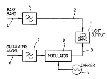
Referring to the drawings, Fig. 1 shows the
transmitter of the optical fibre transmission system, the
transmitter including an LED 1 for launching optical
signals into an optical fibre (not shown). The optical
transmission system operates at 850nm and has a power
reduction of 3dB at 18MHz. The LED 1 is driven by clock
signals (via an input line 2) and by modulated data
signals (via an input line 3), the clock signals and the
data signals being in separate regions of the RF
~0 spectrum. The clock signals and the data signals are
provided by an externally-clocked data test set providing
clock signals and non return to zero (NRZ) data signals as
a pseudo random bit sequence (PRBS) over the range lOOkHz
to 2.5MHz. The clock signals are fed to the line 2 from
~5 an input line 4 via a 3rd order Butterworth low-pass
filter 5 rated at 3 NHz. The data signals are fed to the
line 3 from a data input line 6 via a 3rd order
Butterworth low-pass filter 7 rated at 3 NHz and a Philips
NE 564 modulator 8. The modulator 8 uses coherent
frequency shift keying (coherent FSK) to modulate the data
signals onto a carrier of frequency 7.35 MHz which is
input to the modulator by an oscillator ~. Thus, by
modulating the data signals onto the carrier, and
transmitting the clock signals as a baseband signal, clock
W O 90/10979 PCT/GB90/00406
i ~ 4~ 6 ~ 6 - 6 -
and data are transported independently. The filters 5 and
7 limit the frequency content of the modulated transmitted
optical signal, which leads to a reduction in the sideband
signal and hence helps prevent crosstalk.
The receiver (see Fig. 2) includes an optical receiver
10 which converts optical signals carried by the optical
fibre into electrical signals on a line 11. These
electrical signals are amplified by a National LN733
amplifier 12. The output of the amplifier is fed, in
parallel, to a 3rd order Butterworth low-pass filter 13
rated at 3 MHz, and to a 4th order Butterworth band-pass
filter 14 having a pass range of from 5 MHz to 11 NHz.
The filter 13 extracts the clock signals, and the filter
14 extracts the carrier modulated by the data signals.
The extracted clock signals are amplified by a National
LM733 amplifier 15 whose output is fed to one input of a
D-type flip-flop 16. The extracted carrier/data signals
are passed to a Philips NE564 demodulator 17 which
extracts the data signals from the carrier and feeds them
~ to the other input of the flip-flop 16. The flip-flop 16
synchronises the clock and data signals at its outputs 18.
By modulating the carrier with the data signals, and
transmitting the clock signals as a baseband signal, the
two types of signal are transported independently.
'5 Consequently, there is no requirement for narrow band-pass
filters for extracting the clock components at different
operating rates, so that the system described above
provides simultaneous clock and data transport at variable
transmission rates.
Fig. 3 is a graph showing the optical sensitivity
(which is a measure of the received optical power) against
data rate. For each data rate, the received optical power
is adjusted to obtain a bit error rate (B B ) of
1 x 10 5). The graph shows a generally constant system
W O 90/10979 P ~ /GB90/00406
_ 7 ~ 6 1 6
sensitivity of -42 dBm up to a data rate of about lMb/s.
At higher data rates, a roll-off in sensitivity occurs as
a result of a combination of performance - limiting
factors, a rapid deterioration occuring after the data
rate reaches about 2 Mb/s.
The performance - limiting factors referred to above
are:-
a) Crosstalk
As the transmitted data rate is increased, the
bandwidths of the baseband and modulated signals
increase. At some rate, they will have bandwidths that
begin to overlap. It will then be impossible to separate
the two channels, without observing some degree of
interference between them. This interference manifests
5 itself as jitter, and causes system errors. Crosstalk is
reduced by the use of the low pass filters 5 and 7.
b) Modulated bandwidth
Using FSK for modulation, the ratio fd/r (where fd
is the frequency deviation and r is the data rate) is a
O useful parameter when discussing the bandwidth and power
spectral density (psd) of the modulated signal. For low
values of fd/r (e.g. 0.3), the FSK psd has a peak at the
carrier frequency (fc) with smooth roll-off. The
bandwidth is of the order of 2r. As fd/r increases, the
~5 bandwidth extends beyond 2r, and the psd displays two
peaks at the deviated frequencies fc~fd and fC+fd-
By pre-filtering the transmitted signals, these rates
are attenuated on the band edge of the filter. This leads
to a reduced sensitivity at higher rates, with a roll-off
related to the filters 5 and 7 in the transmitter, as well
as to the filters 13 and 14 used to separate the channels
in the receiver.
W O 90/10979 ~ PCT/GB90/00406
,~,~"~6~ - 8 -
c) Phase relationship
8ecause the clock is not recovered from the same
signal as the data, but is transported independently, it
will suffer delays through the various filters and
recovery processes from those experienced by the data, and
this relative delay varies as the data rate is changed.
Clock edges occuring too soon or too late relative to the
centre of the data 'eye' will result in a sensitivity
penalty, if set up and hold times of any re-timing element
are not met.
A technique, such as automatically inverting the
clock, could be used to overcome this problem. Thus, when
one edge of the clock is too close to the data cross-over,
inverting the clock shifts its phase, by n radians,
towards the centre of the data 'eye'. Either inverted or
non-inverted clock should ensure no noticeable errors due
to poor relative phase of the data and clock.
The penalty paid in using higher order filters with
steeper roll-offs to limit or recover the channels, is the
effect on the group delay of the filters; a higher order
filter having, in general, a larger peak in the group
delay, where the filter begins to roll-off. This leads to
large variations in the phase difference of the data and
clock at the re-timing D-type flip flop 16.
d) Linearity
It is essential that, once the two signals are
combined, the transmission system is linear, until after
the signals are split in the receiver. This avoids
interference between the two channels, due to changes in
their frequency spectra caused by non-linearities. The
optical transmitter and receiver are designed to be
linear, to have no notireAhle affect on the transmitted
spectrum.
W O 90/10979 PCT/GB90/00406
- 9 - 2048616
e) Nodulation/demodulation
The abilities of the modulator 8 and the demodulator
17 to transmit and recover the modulating signal
eventually imposes a restriction on the maximum data rate
r, due to r being too high a percentage of fc- This is
an inherent limitation of the system.
f) Carrier/frequency
A major source of impairment as the transmission rate
is increased is the interference between the baseband and
carrier signals.
The modulation index of the carrier signal is,
therefore, chosen to yield optimum error performance at
the approximate maximum rate. Thus, if T is the period of
the modulating signal, Wc is the carrier frequency, and
Wd is the single-sided frequency deviation, it can be
shown that the minimum probability of an error occurs when:
2WdT = 3n/2,
assuming that WCT>> 1 and Wc>>Wd
For a system operating at maximum rate of 2Nb/s, a
frequency deviation, fd, of approximately 750 kHz is the
theoretical optimum. To maintain the validity of the
assumption that Wc>> Wd, the optimum carrier
frequency for 2Mb/s operation is in the region of 7.5 NHz,
this leading to the choice of 7.35 NHz for the carrier
frequency in the system described above.
The major contributor to the system limitation is the
crosstalk between the ch~nnel~. The crosstalk from the
baseband channel (clock) to the carrier channel, has a
slightly greater effect than that from the carrier channel
to the baseband channel, probably because the clock
harmonics in the region of the carrier frequency are of
larger amplitude than that of the modulated signal at the
clock frequency.
W O 90/10979 P ~ /GB90/00406
204861~ - lO-
The modulation/demodulation process operates
successfully at data rates beyond 2 Mb/s. For example, a
bit error rate less than 1 x 10 8 is achieved at a data
rate of 2.2 Mb/s, when the received optical power is -34
dBm.
The system shown in Figs. 1 and 2 is a simplex system
which could be used in an information - providing
service. In this case, a single transmitter would service
a plurality of receivers via a passive optical network
(PON). Alternatively, where duplex operation is required,
transceivers would be coupled to a PON, each transceiver
being consituted by a combination of the transmitter of
Fig. 1 and the receiver of Fig. 2.
The system described above could be modified in a
number of ways. For example, the data signals could be
the baseband signal, and the clock signals could be
modulated onto the carrier. The 'clock on carrier' system
exhibits similar characteristics to the 'data on carrier~
system, the overall sensitivity being -38dBm. In addition
~O to the crosstalk between channels, however, the
modulation/demodulation process limits the system
performance. This is because of the nature of the
spectrum of a clock signal, and that of a signal when
modulated by the clock. Thus, the clock information is
~5 mainly contained in a single frequency at the clock rate;
and, when this is used to modulate the carrier, the
bandwidth of the modulated signal is wider than in the
case of data modulating the carrier. Clock information is
then lost when the carrier channel band-pass filter 14
attenuates important components of the modulated signal,
resulting in reduced sensitivity. In order to achieve
similar performance to the Idata on carrier' technique,
the 'clock on carrier' system would require a higher
carrier frequency, and a wider band-pass filter in the
receiving circuitry, leading to overall wider system
bandwidth.
W O 90/10979 P ~ /GB90/00406
~ - 11 - 20~8616
Although FSK is the prefered modulation technique,
other methods of sub-carrier multiplexing (frequency
division multiplexing) could be used instead. Moreover,
the technique of sub-carrier multiplexing could be
extended to provide LAN users with a series of flexible
networks, using the same transmission system, by
transmitting the signals from various items of office
equipment on different carrier frequencies. The use of
optical fibre in the LAN, and in the in-building
environment, can thus be made more economical.
It will be apparent that the system described above
enables simultaneous transport of clock and data signals
at variable rates of transmission. This is particularly
advantageous in LANs which exploit the potentially
enormous bandwidth of an optical fibre transmission
system. Thus, using the system described above, many
different signals from different sources could each be
assigned a carrier frequency, and transported through the
same optical fibre. At the receiver, various filters
~0 could pick off the desired carriers, which would undergo
a demodulation process, to provide the user with the
associated data signal. The system could also be used to
provide an upgrading facility, allowing extra transmission
capacity to be provided, without the need to change an
existing transmission network.
Faster electro-optic devices will, in general be
required for the variable rate system described above, as
compared to the electro-optic devices used in conventional
systems operating at the maximum data rate of the variable
system. As demand for suitable electro-optic devices for
LANs increased, so the cost penalty for the extra speed
should reduce, meaning greater network flexibility at
little extra cost.