Note: Descriptions are shown in the official language in which they were submitted.
- ~ 2048933
CARRIER AQUISITION APPARATUS FOR
DIGITAL SATELLITE COMMUNICATION SYSTEM
BACKGROUND OF THE INVENTION
The present invention relates to a carrier aquisition
apparatus for recovering the carrier from a received
burst in a digital satellite communicatlon system, and
more particularly to a carrier recovery apparatus for
recovering the carrier at high speed from the receive
burst having undergone a significant frequency offset
relative to the transmission speed of digital signals.
In a burst mode digital satellite communication
system, it is necessary to promptly synchronize the
reference carrier with the carrier component of the
receive burst transmitted from another ground station
via a satellite, and recover data from modulated digital
data, for instance phase shift keying modulated data,
contained in the received burst. For this reason, there
are arranged in the received burst, preceding the transmit
data section, a carrier recovery sequence for recovering
the carrier, a bit timing recovery sequence for recovering
the bit timing and a~unique word for indicating the
beginning of the transmitted data. In order to correctly
recover the unique word and the data sequence from the
receive burst, it is necessary not only to correctly
extract a bit timing signal from the bit timing recovery
- 2 - 20~893~
sequence but also to promptly synchronize the reference
carrier with the frequency and phase of this carrier
recovery sequence while the carrier recovery sequence
is being received.
A phase-locked loop (PLL) is used for this carrier
recovery. For examples of this PLL, reference may be made
to Namiki, Otani and Yasuda, "0 dB Eb/No Burst Mode SCPC
Modem with High Coding Gain FEC" in the 1986 INTERNATIONAL
CONFERENCE ON COMMUNICATION, and F.M. Gardner, Phaselock
Techniques (1979, John Willey & Sons, Inc.) among others.
In a communication process in which signals are
transmitted via an artificial satellite, a frequency
offset occurs from the remaining effect of automatic
frequency control (AFC) or the drift of the oscillator
on the transmitting side. The maximum frequency offset
can be typically in a usual satellite communication
system. In low modulation rate burst signal t~ansmission,
however, the carrier offset becomes a serious problem
for carrier recovery, as will be described below.
Here is supposed a case where a first order PLL is
used which comprises a phase detector, a voltage controlled
oscillator, and a loop filter whose transfer function
F(s) = 1. This first order PLL is characteristic in
that the acquisition time is short even when the carrier
power-to-noise ratio is low. Then suppose a case in
which there is a frequency difference ~w (= 2~f) between
- 3 - 2048933
the carrier component of the received burst and the
reference carrier. For the first order phase lock loop
with a sinusoidal characteristic phase detector, the
equation representing the response of a phase error
~e(t) between the input carrier phase and the reference
carrier phase is:
d~ (t)
det = ~w - K sin~e(t) .... (1)
where K is the loop gain. In order to achieve a steady
d~e(t)
state of ( dt = ) In order to achieve phase lock,
the relationship of
¦ K ¦ ¦ K ¦ < 1 .... (2)
is required as derived from Equation (1). Therefore, if
the frequency offset ~f exceeds 2K~ , the PLL will become
unable to be phase-synchronized with the input signal,
making it difficult for the carrier to be recovered.
Although the permissible frequency deviation ~w can be
increased if the loop gain K is enlarged, a greater K
would invite an increase in the phase jitter of the
reference carrier, and therefore there is a certain
limit to the enlargement of K. Accordingly, a wide
frequency range for carrier acquisition cannot be
covered by a single PLL. If the loop gain of the first
order PLL is made 0.1-2~fb when the modulation rate is
fb (baud), the frequency offset which permits pull-in
2048933
4 66446-511
by a PLL will bel~f¦ ~ 0.1 fb. Then, in low rate transmission of
fb = 1200 to 9600 (baud), the upper limit of the frequency offset
synchronizable by a phase synchronizing circuit will be 120 to 960
Hz. Therefore, it would be difficult to recover, with a single
phase synchronizing circuit, the carrier from a received burst
having a frequency offset of as great as 2 kHz.
A conceivable solution to this problem is parallel
processing, i.e. a method using a plurality of demodulators having
a different pull-in range from each other and obtaining
demodulated signals from the demodulator having detected the
greatest carrier component. This method, however, requires large
hardware, because of the need for a plurality of demodulators, and
accordingly is uneconomical.
SUMMARY OF THE INVENTION
An object of the present invention, therefore, is to
provide a carrier acquisition apparatus capable of promptly
recovering the carrier from the received burst without requiring
large hardware even in burst transmission in a satellite
communication system in which exists a frequency offset of a
magnitude surpassing the data modulation rate.
According to the invention, there is provided an
apparatus for carrier acquisition, from receive burst signals in a
digital satellite communication system, comprising:
demodulating means for demodulating said receive
burst signals on the basis of a reference carrier and supplying
demodulated signals;
~;',~`'
_ 5 2 ~ 4 8 9 33 66446-511
phase difference detecting means for detecting a
phase difference between a carrier component of said receive burst
signals and said reference carrier on the basis of said
demodulated signals, and supplying a phase difference signal;
first filtering means for filtering said phase
difference signal from said phase difference detecting means, and
supplying a phase control signal;
frequency control signal generating means for
generating a frequency control signal on the basis of a first
control signal;
reference carrier generating means for generating
said reference carrier on the basis of said phase control signal
and said frequency control signal, said reference carrier
generating means having built-in memory means for storing a
control value of said phase control signal and said signal
frequency control signal, said control value being stored at an
address defined by said first control signal;
second filtering means for filtering said
demodulated signals, and supplying filtered demodulated signals;
D.C. value calculating means for calculating a D.C.
value contained in said filtered demodulated signals;
unmodulated carrier component detecting means for
detecting the greatest value of said D.C. value calculated by said
D.C. value calculating means; and
control means for circulatively controlling said
first control signal to change said frequency control signal in
part of the period of a carrier recovery section of said burst and
,~,t,l
20~8933
6 66446-511
when no burst has been received yet, and for supplying an optimal
control signal of said first control signal associated with said
greatest value of said D.C. value, wherein said digital satellite
communication system operates by a reference carrier generated by
said reference carrier generating means in accordance with said
optimal control signal.
BRIEF DESCRIPTION OF THE DRA~INGS
Figure 1 is a block diagram illustrating the
configuration of a preferred embodiment of the present invention.
Figure 2 is a timing chart roughly illustrating the
operations of the configuration of Figure 1, wherein:
Figure 2A shows the composition of the receive burst;
Figure 2B, the data clock which is the timing signal of
data in the receive burst;
Figure 2C, clock periods and split periods in the time
division PLL processing according to the invention;
Figure 2D, operational clock;
Figure 2E, a data reception end (DEND) signal; and
Figure 2F, a control signal START.
Figure 3 is a block diagram illustrating the
configuration of a complex multiplier.
, ~,tj
~'
7 2048933
FIG. 4A is a block diagram illustrating a digital
VCO circuit and a memory accompanying it.
FIG. 4B is a timing chart for describing the
operation of the circuit of FIG. 4A.
FIG. 5 is a block diagram illustrating the
configuration of a low-pass filter.
FIG. 6 is a block diagram illustrating the
configuration of an unmodulated carrier detecting
circuit.
FIG. 7 is a flow chart for describing the operation
of the control circuit.
DESCRIPTION OF THE PREFERRED EMBODIMENT
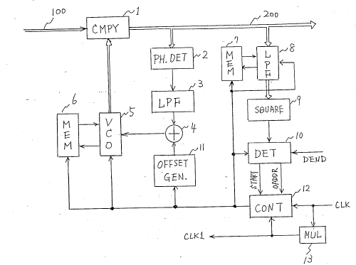
FIG. 1 is a block diagram illustrating the
configuration of a preferred embodiment of the present
invention. This embodiment is provided with a complex
multiplier 1 for detecting a quasi-coherent detected
receive burst signal 100 with a reference carrier
supplied from a digital VCO 5 and supplying an in-phase
signal I, which is the in-phase component of a demodulated
signal 2Q0, and an quadrature signal Q, which is the
quadrature component of the demodulated signal 200; a
phase difference detector 2 which is supplied with the
demodulated signal 200 and obtains the phase difference
between the carrier component of the receive burst
signal 100 and the reference carrier supplied from the
- 8 - 20~8933
digital VCO 5; and a low-pass filter for filtering this
phase difference to obtain a phase control signal.
The preferred embodiment of the invention is also
provided with an offset generator 11 for supplying a
frequency control signal on the basis of an address
signal (ADDR) supplied from a control circuit 12; an
adder 4 for adding the phase control signal and the
frequency control signal to supply a frequency-phase
control signal; the digital VCO 5 for supplying the
in-phase component and the orthogonal component of
the reference carrier on the basis of the frequency-
phase control signal; and a memory 6 for storing the
internal value of the digital VCO 5 or setting the
internal value on the basis of a control signal from
the control circuit 12.
The embodiment is further provided with a low-pass
filter 8 for filtering the in-phase signal I and the
quadrature signal Q, and supplying a filtered in-phase
signal I' and a filtered quadrature signal Q'; a memory
7 for storing the internal value of the low-pass filter 8
or setting a stored value in the low-pass filter 8 on the
basis of a control signal from the control circuit 12;
a square-sum circuit 9 for calculating a sum (I~2 + Q~2)
of the squares of the filtered in-phase signal I' and
the filtered orthogonal signal Q', and supplying the
sum as a calculated value indicating the magnitude of
9 2048933
the digital VCO output frequency component contained in
the receive burst; and an unmodulated carrier detecting
circuit 10 which is supplied with the calculated value
and an address corresponding to this calculated value,
holds the address at which this calculated value reaches
its maximum (OADDR), and supplies a control signal START
indicating the end of data reception and the start of
the reception of the carrier recovery section of the
receive burst.
Still further, the embodiment of the invention is
provided with a control circuit for generating control
signals including the control signal ADDR on the basis
of the control signal START supplied from a squaring
circuit 9, a data clock and an operational clock, both
to be explained later, and controlling the operations
of the digital VCO 5, the memory 6, the offset generator
11 and the low-pass filter 8. -
In addition to the foregoing, the embodiment isprovided with a multiplier 13 for multiplying the clock
of the data in the receive burst, i.e. data clock (CLK),
and generating operational clock (CLKl) for operating
the digital VCO 5, the low-pass filter 8 and the control
circuit 12 etc.
The configuration of the preferred embodiment of the
present invention illustrated in FIG. 1 has been summarized
above. Before describing internal embodiments of elements
2048933
-- 10 --
in Fig. i, the principle of the invention will be explained
below with reference to FIGS. 2A through 2F.
FIG. 2A shows the composition of the receive burst;
FIG. 2B, the data clock; FIG. 2C, the control signal ADDR;
FIG. 2D, the aforementioned operational clock (CLK1);
FIG. 2E, the DEND signal indicating the completion of
the demodulation of the receive burst; and FIG. 2F, the
control signal START.
As illustrated in FIGS. 2A to 2C, according to the
present invention, the period of receiving the carrier
recovery section of the receive burst is split into a
time division phase locked loop (PLL) operation period
(TD.PLL.OP. in FIG. 2C) and a conventional PLL operation
period (PLL.OP. in FIG. 2C), both to be explained later.
The period in which the bit timing recovery sequence,
unique word and data section are entered is the
conventional PLL operation period, and time di~ision PLL
operation takes place in the period after the completion
of data reception, during which no burst is received.
The time division PLL operation period, while the
carrier recovery section of the burst is received, is
divided into M clock periods each of which is either
one data clock or one cycle of modulated clock (the 1st
throu~h Mth clock periods in FIG. 2C), and each clock
period is further divided into N subperiods #0, #1, ....
#N-l.
11- 2048933
Now, the digital VCO is so set as to make the
frequency lead-in range of the PLL in the subperiod
2 0 - ( 2 + 1) ~f + fO, where + N2 ~f is
the maximum frequency offset, which may be +2 kHz
for instance, and fO is the carrier frequency at a
frequency offset of 0 Hz. It also is so set as to
make the frequency lead-in range in the subperiod
#i (~ 2 + i) ~f + fo ~ f ~ (- 2 + i + 1) ~f + fO, and
that in the subperiod #(N-1) (N2 - 1) ~ f ~ f < N2 ~f + fo'
with the result that a maximum frequency offset range
f ~ 2 ~f + fo -< f < 2 ~f + fo~ i-e- If ~ fO¦ < 2 kHz,
is covered in the subperiods #0 through #(N-l).
When a burst signal having a frequency offset is
supplied to the carrier acquisition apparatus of the
lS invention, the closer the subperiod to which a frequency
pull-in range is allocated to the carrier frequency of
the burst, the sooner the carrier phase synchr-onization
is performed. Whereas a D.C. component is generated
when the carrier recovery section of the receive burst
is orthogonally detected with the output of the VCO,
the magnitude of this D.C. component reaches its maximum
when the unmodulated carrier of the carrier recovery
section in the receive burst and the recovered carrier
supplied from the VCO become synchronized in phase.
According to the invention, the magnitude of this
D.C. component is monitored for each subperiod, and the
- 12 - 20189~3
subperiod in which the D.C. component takes on its greatest
magnitude (the optimum subperiod) is detected in the Mth
clock period, i.e. the final clock period of the time
division PLL operation period. Further according to the
invention, the frequency pull-in range of the VCO is set
to that of optimum subperiod upon entrance into the
convention PLL operation pull-in range, and the process
shifts to the conventional PLL operation. In this way,
there can be realized a carrier acquisition apparatus
which promptly establishes carrier synchronization even
for the carrier of a burst signal of a large frequency
offset and a low bit rate without having to enlarge the
hardware dimensions extremely.
Now will be described, referring back to FIG. 1,
the operation of the preferred embodiment of the present
invention.
A quasi-coherently detected receive burst~-is
multiplied in the complex multiplier 1 by the in-phase
component and the quadrature component of a recovered
carrier supplied from the digital VCO 5 to give the
in-phase component I and the quadrature component Q
of a demodulated signal 200, respectively. The
demodulated signal is supplied to the phase difference
detector 2 and the low-pass filter 8.
The phase difference detector 2 detects the phase
difference between the reference carrier supplied from
_ - 13 - 2048933
the digital VCO 5 and the carrier component of the receive
burst 100 on the basis of the in-phase signal I and the
quadrature signal Q. For the configuration of this phase
difference detector, reference may be made to, for instance,
F.M. Gardner, Phaselock Techniques (1979, John Willey &
Sons, Inc.), Fig. 11.9 and elsewhere.
The phase difference detected by the phase difference
detector 2 is filtered by the low-pass filter 3 to give
a phase control signal, which is added to a frequency
cor.trol signal supplied from the offset generator 11,
and the resultant frequency-phase control signal is
supplied to the digital VCO 5.
In the offset generator 11, composed of a read only
memory (ROM) for instance, is written in advance the
frequency control signal corresponding to a subperiod-
indicating address ADDR (#0 to #N-l) supplied from the
control circuit 12. This ROM outputs a stored~-value as
the frequency ccntrol signal corresponding to the address
ADDR supplied from the control circuit 12 (this address
indicates a subperiod), and supplies the frequency
control signal to the adder 4.
The digital VCO 5 generates the in-phase component
and the quadrature component of the reference carrier
on the basis of the frequency-phase control signal, and
supplies them to the complex multiplier 1. The internal
configuration and operation of this digital VCO 5, which
- 14 - 2048933
will be described in more detail below, differ from those
of a conventional digital VCO in that the internal value
is updated at the beginning time of each of the subperiods
#0 through #N-l to the internal value at the ending time
of the same subperiod of the preceding cycle (this value
is stored in the memory 6), so that continuous operation
apparently takes place at the same subperiod. Thus the
digital VCO 5, based on a value stored from the memory 6
at the beginning time of each subperiod, outputs the in-
phase component and the orthogonal component of therecovered carrier, within the frequency pull-in range
assigned to each subperiod, in accordance with the
frequency-phase control signal entered from the adder
circuit 5.
In the aforementioned conventional PLL operation
period, at the beginning time of the period, the internal
value of the digital VCO is set, in accordance~with a
control signal from the control circuit 12, to the
internal value at the ending time of the period determined
to be the aforementioned optimum subperiod in the Mth
clock period. The offset generator 11, supplied with
an address indicating this optimum subperiod from the
control circuit 12, generates a frequency control signal
in the optimum subperiod. In this way, this embodiment
of the invention performs operation, after the completion
of time division PLL operation and until that of the
_ - 15 - 2048933
-
reception end of the data section in the receive burst,
in the conventional PLL operation period.
As described above, the loop consisting of the complex
multiplier 1, phase difference detector 2, low-pass filter 3,
adder 4 and digital VCO 5 performs time division PLL and
conventional PLL operations in accordance with the control
signal from the control circuit 12.
Meanwhile, the in-phase signal I and the quadrature
signal Q outputted from the complex multiplier 1 are
supplied to the low-pass filter 8, cleared of their
respective high frequency ccmponents, and converted into
the filtered in-phase signal I' and the filtered quadrature
signal Q'. They are supplied to the squaring sum circuit 9,
which calculates the sum of squares (Il2 + Ql2). As is
well known to those skilled in the art, this calculated
value serves as the D.C. value to indicate the magnitude
of the digital VCO's output frequency component in the
carrier of the carrier recovery section of the burst.
This calculated value is almost zero except in the carrier
recovery section of the receive burst or in a period in
which no burst is received.
The unmodulated carrier detecting circuit 10 is
supplied with the aforementioned calculated value and
the data reception end signal (DEND). The signal (DEND)
indicates the completion of the operation to receive
the data section of the received burst, and is supplied
_ - 16 - 2048933
from a receive data processing circuit (not shown) arranged
downstream in this preferred embodiment. The internal
configuration of this unmodulated carrier detecting circuit
10 will be described later.
Upon arrival of the DEND signal (see FIG. 2E), the
unmodulated carrier detecting circuit 10 supplies the
control circuit 12 with the control signal START to
instruct ending of the conventional PLL operation then
under way and shifting to the time division PLL operation
(see FIG. 2F). When the output of the squaring circuit 9
exceeds a prescribed threshold for the first time during
the period of time division PLL operation, the unmodulated
carrier detecting circuit 10 reverses the polarity of
the aforementioned control signal START and notifies
the control circuit 12 that the time division PLL
operation should be ended M clock periods later. What
is to be noted here is that the first surpassing of the
prescribed value by the output of the squaring circuit 9
during the period of time division PLL operation means
that the leading part of the carrier recovery section of
the receive burst has been received. The operations
according to the present invention assume this detection
time to be the time of burst reception.
The unmodulated carrier detecting circuit 10 is
supplied with calculated values successively coming from
the squaring circuit 9, i.e. D.C. values indicating the
- 17 - 20~8933
magnitudes of components in the receive burst synchronized
with the recovered carrier. The unmodulated carrier
detecting circuit 10 holds the address indicating the
subperiod at which the D.C. value fed after the completion
of the data reception of the previous receive burst was
at its greatest among the subperiods of time division PLL
operation, i.e. the optimum address (OADDR). Thus the
optimum address is held within the unmodulated carrier
- detecting circuit 10 at the ending time of time division
PLL operation, i.e. that of the Mth clock period and of
the final subperiod in FIG. 2C, and this optimum address
(OADDR) is supplied to the control circuit 12.
The control circuit 12 starts time division PLL
operation upon transition of the control signal START
(FIG. 2F), supplied from the unmodulated carrier detecting
circuit 10, to a low level. It generates control signals
to control the operations of the digital VCO 5,~ memories
6 and 7, low-pass filter 8 and unmodulated carrier
detecting circuit 10 on the basis of the data clock CLK
(see FIG. 2B) from a data clock regenerating circuit
arranged downstream in this embodiment and the operational
clock CLKl (see FIG. 2D) generated by multiplying the
data clock with the multiplier 13.
When the control signal and the START signal shown
in FIG. 2F come down to a low level, the control circuit 12
successively generates control signals ADDR to designate
_ - 18 - 2048933
subperiods #0, #1, ..., #(N-l) on the basis of the data
clock CLK and the operational clock CLKl to cause the
digital VCO 5, offset generator 11 and low-pass filter 8
to perform time division operation for each subperiod.
Thus the offset generator 11 is caused to output a
frequency control signal corresponding to the pertinent
subperiod, and the digital VCO 5 to oscillate in the
frequency pull-in range allocated for the subperiod.
The control circuit 12 further causes the internal values
of the digital VCO 5 and of the low-pass filter 8 to be
stored in the memories 6 and 7, respectively, at the final
operational clock time of each subperiod. This operation,
as will be explained later, is accomplished by raising a
control signal R/W to a high level.
In addition, the control circuit 12 causes the
internal values of the digital VCO 5 and of the low-pass
filter 8 at the ending time of the same subper~od in the
immediately preceding clock period, which are stored in
the memories 6 and 7, to be stored in the digital VCO 5
and the low-pass filter 8 at the beginning time of each
subperiod. In this way, the initial value of each circuit
at the first operational clock (CLKl) time of each
subperiod is determined so that the time division
operation can be smoothly performed.
When the control signal rises to the high level,
i.e. when the carrier recovery section of the receive
20~8933
burst is detected, the control circuit 12 ends the time
division PLL operation M clock periods later. The
operation of the control circuit 12 during these M clock
periods is the same as that during the period when no
burst is received as yet.
At the end of the final subperiod of the time division
PLL operation, i.e. at the end of the #(N-l) subperiod of
the Mth clock period in FIG. 2C, the control circuit 12
sends the address signal (OADDR) indicating the optimum
subperiod supplied from the unmodulated carrier detecting
circuit 10 to the offset generator 11 to cause it to
supply the frequency control signal corresponding to the
optimum subperiod. This address signal is also sent to
the memories 6 and 7, and the internal values of the
digital VCO 5 and the low-pass filter 8 at the final
operational clock time in the Mth clock period are set in
the digital VCO 5 and the low-pass filter 8, respectively.
After that, conventional PLL operation takes place within
the frequency pull-in range corresponding to the address
OADDR until the reception of all the data in the data
section of the receive burst is completed, i.e. until the
aforementioned DEND signal is supplied to the unmodulated
carrier detecting circuit 10.
What should be noted here is that, when no burst
has been received as yet and at the time of receiving
the carrier recovery section of the burst, the bit timing
- 20 - 204~9~3
recovery section of the receive burst has not yet been
received, so that the data clock (CLK) supplied from the
data clock regenerating circuit (not shown) arranged down-
stream in this embodiment is not in phase-synchronism with
the data timing signal of the data section in the burst.
However, as the output of the data clock regenerating
circuit, though no in synchronism with the data timing
signal of the data section in the burst, is freely
oscillating at a frequency very close to its frequency,
accordingly there is no obstacle to practical use.
Although the foregoing description assumed that a
quasi-coherently detected receive burst was entered, the
present invention can be similarly executed even if a
receive burst which is frequency-converted into the IF
band is entered.
FIG. 3 illustrates the configuration of the complex
multiplier 1. The in-phase component x(t) of t-he quasi-
synchronously detected receive burst is supplied to
multipliers 21 and 22 via a signal line 100-1, while the
quadrature component y(t) of the quasi-coherently detected
receive burst is supplied to multipliers 23 and 24 via a
signal line 100-1.
Meanwhile, the multipliers 21 and 24 are supplied
with the in-phase component cos 2~ ft of the recovered
carrier, while the multipliers 22 and 23 are supplied
with the quadrature component sin 2~ ft of the recovered
- 21 - 2Q~8933
carrier. The outputs of the multipliers 21 and 23 are
added by an adder 25 to give x(t) cos 2~ ft + y(t) sin2~ ft,
which represents the in-phase component I of the demodulated
signal and is outputted to a signal line 200-1.
A subtracter 26 subtracts the output of the
multiplier 22 from that of the multiplier 24, resulting
in - x(t) sin2~ ft + ~(t) cos 2~ ft, which represents the
quadrature component Q of the demodulated signal and is
outputted to a signal line 200-2.
Next will be described the configurations and
operations of the VCO 5 and the memory 6 with reference
to FIGS. 4~ and 4B. The frequency-phase control signal
supplied from the adder 4 is multiplied by KV in a
multiplier 30, where Kv is a constant which determines
the modulation sensitivity of the VCO. The Kv-multiplied
frequency-phase control signal is accumulated by an
accumulator consisting of an adder 31 and a register-
equipped multiplexer (REG) 32. The result of accumulation
is supplied as an address to read only memories (ROM s)
33 and 34.
In the ROM'S 33 and 34 are stored a one-cycle
equivalent each of cosine and sine waves, respectively.
When the address is fed to the ROM's, the cosine wave is
outputted from the ROM 33, and the sine wave, which has
a phase lag of ~/2 from the cosine wave, from the ROM 34,
both being fed to the complex multiplier 1 of FIG. 1.
- 22 - 20~8933
The hitherto described are the operations which take place
in each subperiod and when the time division PLL has
shifted to a single-channel operation after the completion
of time division operation. At this time, a control signal
SEL from the control circuit 12 of FIG. 1 so effects
control as to make the register-equipped multiplexer 32
take in the output of the adder 31.
Now will be described the operations at the end and
beginning of each subperiod with reference to the timing
chart of FIG. 4B. To the memory 6 are supplied an address
signal ADDR indicating the subperiod (FIG. 4B(a)) and a
R/W signal which has entered into a write instructing
state (high level) (FIG. 4B(c)), and the value of the
register-equipped multiplexer 32 is written into the
memory 6.
At the beginning time of each subperiod, the R/W
signal is in a read state (low level), and the~-value of
the register-equipped multiplexer 32 at the ending time
of the same subperiod in the preceding cycle is outputted
from the memory 6. At this beginning point of a subperiod,
the control signal SEL from the control circuit 12 is at
a high level, and the register-equipped multiplexer 32
takes in the value outputted from the memory 6. In this
way, the initial phase of the VCO 5 at the beginning point
of each subperiod is determined.
At the time when the operation as time division PLL
- 23 - 20~8933
has ended, i.e. at the first operational clock time of
conventional PLL operation, the address indicating the
optimum subperiod (OADDR) is fed from the control circuit
12 to the memory 6, which outputs the value of the
register-equipped multiplexer 32 at the final operational
clock time of the optimum subperiod of the final cycle of
time division PLL. At this operational clock time of
conventional PLL operation, the control signal SEL from
the control circuit 12 again rises to the high level,
and the output of the memory 6 is taken in by the register-
equipped multiplexer 32. After that, the control signal
SEL again falls to the low level, and the register-equipped
multiplexer 32 again takes in the output of the adder 31.
The value of the control signal ADDR is fixed at the
address indicating the optimum subperiod. In this manner,
the PLL shifts to the operation of the VCO similar to
conventional PLL operation. ~
Next will be described the configurations and
operations of the low-pass filter 8 and the memory 7
with reference to FIG. 5. As shown in FIG. 5, the
low-pass filter 8 is composed of an in-phase signal
filter 8-1, to which an in-phase signal is supplied, and
an quadrature signal filter 8-2. The in-phase signal
filter 8-1 and the quadrature signal filter 8-2 are
supplied with the in-phase component I and the quadrature
component Q of the demodulated signal, outputted from the
- 24 - 20~893~
complex multiplier 1 of FIG. 1, via signal lines 200-1
and 200-2, respectively. The memory 7 is divided into
memory 7-1 and 7-2 respectively matched with the in-phase
signal filter 8-1 and the quadrature signal filter 8-2.
Since the configurations and operations of the in-phase
signal low-pass filter 8-1 and the memory 7-1 are
respectively the same as those of the quadrature signal
low-pass filter 8-2 and the memory 7-2, only the former
will be described here.
FIG. 5 illustrates an example in which a transversal
filter is used as the in-phase signal low-pass filter 8-1,
which differs from a conventional transversal filter in that
register-equipped multiplexers 41 and 42 are used as delay
elements. Whereas the in-phase signal low-pass filter 8-1
is supplied with a control signal SEL, and the memory 7-1,
with a control signal ADDR and a control signal R/W, these
signals are the same as the signals to which ~espectively
the same symbols are assigned in FIG. 4.
First, while both the control signal SEL and the
control signal R/W are at the low level, i.e. during
each subperiod of time division PLL operation except the
beginning and ending times, or after time division PLL
has ended and shifting to convention PLL operation has
taken place, the register-equipped multiplexer 41 takes
in the in-phase signal I from the signal line 200-1, and
the register-equipped multiplexer 42 takes in the output
- 25 - 2048933
value of the register-equipped multiplexer 41, the in-phase
signal low-pass filter 8-1 operates in the same way as a
conventional transversal filter. Thus a signal on the
signal line 200-1, the output of the register-equipped
multiplexer 41 and that of the register-equipped
multiplexer 42 are multiplied by weight coefficient wl,
w2 and w3 in multipliers 43, 44 and 45, respectively, and
the outputs of the multipliers 43, 44 and 45 are added by
an adder 46, the sum being supplied as the filtered in-
phase signal.
Next will be described the operation which takes placewhen the control signal SEL from the control circuit 12
is at the low level and the control signal R/W is at the
high level, i.e. at the ending time of each subperiod of
time division PLL operation. As the control signal R/W
is at the high level, memory units 47 and 48 are in the
write mode, and the values of the register-eq~ipped
multiplexers 41 and 42 are written into the memory units
47 and 48 at the address indicated by the control signal
ADDR. These written values are read out at the beginning
time of the same subperiod of the next data clock period.
Now will be described the operation taking place when
the control signal SEL from the control circuit 12 is at
the high level and the control signal R/W is at the low
level, i.e. at the beginning time of each subperiod of
time division PLL operation. At this time, as the memory
- 26 - 20~89~3
units 47 and 48 are in the read mode and the address
indicating the subperiod is given as the control signal
ADDR, the values of the register-equipped multiplexers
41 and 42 of one cycle beofre, i.e. at the ending time of
the same subperiod one modulation clock time before, are
supplied from the memory units 47 and 48. At this time,
as the control signal SEL is at the high level, the
register-equipped multiplexers 41 and 42 take in the
output values of the memory units 47 and 48, respectively.
In this way, in spite of the time division operation of
the in-phase signal filter, continuous operation is taking
place with respect to the same subperiod alone.
At the time immediately after the end of time division
PLL operation, the control signal SEL again rises to the
high level. At this time, as the address indicating the
subperiod judged to be the optimum in the final period
of time division PLL operation is supplied as the control
signal ADDR, the values of the register-equipped
multiplexers 41 and 42 are read out of the memory units
47 and 48, respectively, and taken into the register-
equipped multiplexers 41 and 42. Immediately after this,
the control signal SEL again falls to the low level, and
the control signal ADDR is fixed to the value indicating
the optimum split time, with the filter shifting to
conventional PLL operation.
Although the foregoing description, for the sake of
- 27 - 2048933
simplicity, supposed a case in which three-tapped
transversal filters were used as the low-pass filters
8-1 and 8-2, they are not limited to three-tapped filters.
Next will be described the configuration of the
unmodulated carrier detecting circuit 10 with reference
to FIG. 6. The unmodulated carrier detecting circuit 10
is provided with a register 60 for sampling the calculated
value supplied from the squaring circuit 9 with the
aforementioned control signal R/W; a threshold circuit
comprising a gate 61 and a comparator 62; a maximum value
detecting circuit consisting of a comparator 64, an AND
gate 65 and a register 66; a register 67 for holding the
address corresponding to the maximum value detected by
the maximum value detecting circuit; and a set/reset
flip-flop 63 reset by the control signal DEND supplied
from outside this embodiment and set by the output of the
comparator 62. i~
When the control signal DEND shown in FIG. 2E rises
to the high level, i.e. when the receive data processing
circuit arranged downstream in this embodiment completes
the reception of all the data, the set/reset flip-flop 63
is reset. The output of this set/reset flip-flop 63 is
sent to the control circuit 12 as the aforementioned
control signal START. The control circuit 12 can know
the timing at which the conventional PLL operation
currently under way is to be ended and a shift to time
- 28 - 20~8933
division PLL operation should take place by detecting the
high to low transition of this control signal START from
the high to the low level. As will be described later,
the set/reset flipflop 63 is set by the output of the
comparator 62 at the timing of the leading part of the
carrier recovery section of the receive burst. At this
time, the control signal START undergoes transition from
the low to the high level, and the control circuit 12
can know from this transition that the time division PLL
operation currently under way is to be ended in M more
clock times. This control signal START is also supplied
to the clear terminal of the register 66, which is cleared
while the control signal START is at the low level, i.e.
after the completion of burst reception until the entry
of the leading part of the carrier recovery section of
the next burst.
The value supplied from the squaring circuit 9, i.e.
the calculated value indicating the recovered carrier
frequency component of the receive burst (or the
oscillating frequency component of the digital VCO 5)
is sampled by the register 60 with the control signal
R/W, and fed to the gate 61 and the comparator 62.
The comparator 62 compares the calculated value
supplied from the register 60 with a fixed threshold (TH).
If the calculated value is greater than the threshold,
the comparator 62 will output a high level, or if not,
20~8933
_ - 29 -
a low level. The gate 61 lets the entered calculated value
as it is when the output of the comparator 62 is at the
high level or, when it is not, supplies a value 0 to the
first input of the comparator 64.
The output of the comparator 62 is also supplied to
the set terminal of the set/reset flipflop 63, which is
set when the output of the comparator 62 is at the high
level. Here, the time when the output of the comparator
62 rises to the high level for the first time is at the
leading part of the carrler recovery section of the receive
burst, because it is only when the carrier recovery section
is entered that the output of the squaring circuit 9 can
surpass the threshold (TH). In other words, the threshold
(TH) is so set that the square sum may not surpass it in
any other part of the receive burst or when no burst has
been received yet. If, however, too great a value is
given to this threshold, it will become impossible to
detect the carrier recovery section. Therefore, it is
so selected as to equalize the probability of the square
to be below the threshold in the carrier recovery section
and its probability to surpass the threshold in other
periods.
The operations of the maximum value detecting circuit
consisting of the comparator 64, AND gate 65 and register
66 and of the register 67 are described below. In the
register 66 is stored the greatest among the values entered
_ - 30 -
2o~89~3
in the pàst into the maximum value detecting circuit from
the gate 61. The comparator 64 compares the output of
the gate 61 and that of the register 66. If the output
of the gate 61 is found greater, the output of the
comparator 64 will rise to the high level or, if not,
fall to the low level. The output of this comparator 64
is supplied to the first input terminal of the AND gate 65.
The second input terminal of the AND gate 65 is
supplied with the control signal R/W (see FIG. 4B(c))
from the control circuit 12. Whereas this control signal
R/W, as stated above, rises to the high level only at
the final operational clock time of each subperiod, the
unmodulated carrier detecting circuit 10 generates with
the AND gate 65 timing signals for operating the registers
66 and 67 on the basis of the control signal R/W. The
AND gate 65 lets the control signal R/W pass as it is
when the output of the comparator 64 is at the~-high level.
When it is not, the output of the AND gate 65 is at the
low level. Thus, timing signals are supplied to the
registers 66 and 67 only when the output of the gate 61
is greater than the former maximum value stored in the
register 66. Only when its timing signal is supplied,
the maximum value of the register 66 is updated to the
output value of the gate 61.
Meanwhile, the input of the register 67 is supplied
with the address signal ADDR indicating the subperiod
_ - 31 - 2048933
corresponding to the calculated value supplied from the
squaring circuit 9, and this address signal ADDR is stored
in the register 67 in response to the timing signal from
the AND gate 65. In this way, the address (OADDR)
indicating the subperiod whose calculated value has
become the greatest is held in the register 64. This
address OADDR is read out by the control circuit 12 at
the ending time of the tiem division PLL operation period.
Next will be described the control circuit 12, which
consists of a microprocessor or the like. FIG. 7 is a
flow chart showing the program to be stored in the micro-
processor. The operation of the control circuit 12 will
be described below with reference to this flow chart.
When the power supply to the apparatus is turned on,
the operation of the control circuit begins with time
division PLL operation before any burst has been received,
as shown in steps Sl through S6. The operation from
step Sl through step S6 is repeated until the detection
at step S5 of the transition of the control signal START
from the unmodulated carrier detecting circuit 10 from
the low to the high level.
First at step Sl, the control signal ADDR is set to 0.
Then at step S2, the control signal ADDR is supplied to the
memories 6 and 7, unmodulated carrier detecting circuit 10
and offset generator 11 of FIG. 1. The processing at
this step S2, as stated above, takes place at the first
2048933
- - 32 -
operational clock time of each of the subperiods
#0 through #(N-l). At step S2, the control signal SEL
is raised to the high level, and supplied to the memories
6 and 7, and the internal values of the digital VCO 5 and
the low-pass filter 8 at the final operational clock time
of the same subperiod in the preceding data clock cycle,
stored in these memories, are caused to be stored into
register-equipped multiplexers, in which are stored
internal values, in the digital VCO 5 and the low-pass
filter 8. Upon completion of this processing, the control
signal SEL again falls to the low level.
The~, at the final operational clock time of each
subperiod, the control signal R/W is raised to the high
level at step S3, and the internal values of the digital
VCO 5 and the low-pass filter 8 are stored into the
memories 6 and 7. Upon completion of this processing,
the control signal R/W is again set to the low~level.
At step S4, the value of the control signal ADDR is
increased by 1.
At step S5, upon detection of the transition of the
control signal START from the unmodulated carrier detecting
circuit 10 from the low to the high level, the operation
from step Sl through step S6 is ended, followed by shifting
to the processing of step S7 and thereafter. If this
transition of the control signal START is not detected,
the control moves on to step S6, and it is judged whether
~ ~ 33 ~ 2048933
or the ADDR is N or above. If it is, the control will
return to step Sl, and the processing of one clock period
will be completed. If not, it will return to step S2.
In this way, if the transition of the control signal
START from the low to the high level is not detected,
the processings from step Sl through S6 will be repeated.
Meanwhile, if the transition of the control START
from the low to the high level is detected at step S5,
time division PLL operation from step S7 through step S12
will take place. The processings at steps S8, S9, S10,
Sll and S12 are the same as those at steps Sl, S2, S3, S4
and S6, respectively. By repeating the processings from
step S8 through step S12 M times, control signals required
from time division PLL operation from the first through
Mth clock periods in FIG. 2 are generated.
Upon completion of the processings from step S7
through step S12, there will take place shifti~ng to
conventional PLL operation. First at step 13, the address
(OADDR) indicating the optimum subperiod, supplied from
the unmodulated carrier detecting circuit 10, is directly
outputted as the control signal ADDR. Then at step S14,
the control signal SEL is raised to the high level at
only one operational clock time, and the internal values
of the digital VCO 5 and the low-pass filter 8 at the
final operational clock time of the optimum subperiod
in the Mth clock period are transferred to the register-
_ - 34 -
2048933
equipped multiplexers in the digital VCO 5 and the low-pass
filter 8. In this way, the control circuit 12 moves on
to the control of conventional PLL operation in FIG. 2.
This conventional PLL operation continues until the
transition of the control signal START from the unmodulated
carrier detecting circuit lO from the high to the low
level takes place at step S15, i.e. until the set/reset
flipflop 63 in the unmodulated carrier detecting circuit
10 is reset.
Upon detection of the transition of the control
signal START to the low level at step 15, i.e. upon
completion of the demodulation of the data section of
the receive burst, the control circuit 12 will return
to the processings from step Sl through step S6.