Note: Descriptions are shown in the official language in which they were submitted.
20~9~
REMOTE CONTROL OF FLUORE8CENT LANP R~T-T ~ RT
U~ING POWER FLOW ~ ~KKUPTION CODING WITH MEAN8 TO
MAINTAIN FTT~M~NT VOLTAGE 8UB8TANTIALLY CO~ ANT
A8 THE LAMP VOLTAGE DEC~T~
BACKGROUND OF THE INVENTION
1. Field of the Invention
The present invention relates to remotely controlled
dimmable electronic ballasts for powering gas discharge lamps
and, in particular, to a ballast system which utilizes a power
line interruption coding system and means for controlling the
lamp filament voltage such that as the lamps are dimmed, the
filament voltage is increased.
2. Description of the Prior Art
The fluorescent lamp is designed to be a replacement
for the incandescent lamp. The fluorescent lamp offers very
large energy savings as compared to incandescent lamps. For
example, a 28 watt fluorescent lamp offers the same light as
a 100 watt incandescent lamp. This tremendous energy savings
has been ignored in some applications because of the
nonavailability of appropriate ballasts and control systems.
For example, special lighting in restaurants, hallway lights,
and other areas wherein the light level needs to be controlled
for either energy savings or special effects has in the past
used incandescent lamps with energy-wasteful dimming systems
to obtain the desired effect. Incandescent dimming systems
utilize either variable transformers, triacs or electronic
means. The electronic means are the most cost-effective but
have serious drawbacks in the form of a very low power factor,
low efficiency and increased harmonic generation. The energy
that may be saved by reducing the kilowatts delivered to the
2049075
lamp load is utilized because of a low power factor and high
harmonic generation. Since low power factor and high
harmonics are harmful to the power system, power companies
continue to search for ways to give their customers the
lighting aesthetics they desire while still saving energy.
A dimming system would require adding extra wires in
the wall to connect the controls and switches to the dimming
ballasts. This is generally unacceptable, since it is very
expensive and thus the prior art sought to communicate to the
ballasts in a different manner. Prior art systems involved
using carrier current type communications over the power line.
A well-designed carrier current type system generally will
work reliably in even difficult conditions. However, the
greatest drawback with this type of communication system is
that it is a broadcast system, i.e., signals are transmitted
in all directions along the wires and therefore are required
to carry complex coding information. In addition, the
ballasts themselves are required to have appropriate decoding
or addressing circuitry. The overall modification is costly
and requires a much larger wall switch box to accommodate
the additional equipment. In addition to the communication
problem noted, the prior art has sought to provide cost
efficient techniques for controlling dimming of the
fluorescent lamps. One of the approaches uses-a
frequency change method (shift) to both control the
lamp current (power) and to maintain the lamp filament voltage
substantially constant as the lamps were dimmed in order to
maintain lamp life. Frequency dimming circuitry, however,
adds to the overall cost and complexity of the dimming ballast
system. A less costly prior art technique utilizes a variable
voltage power source to control lamp dimming. However,
filament voltage could not be controlled by a simple circuit
to preserve lamp life, thus making the technique commercially
unfeasible.
Typical of the prior art ballast control systems are
those disclosed in U.S. Patent No. 4,717,863 to Zeiler wherein
204907~
a frequency modulated circuit is utilized to provide a
variable voltage to dim the fluorescent lamp, an optical
feedback system being utilized to regulate the frequency of
the output signal; U.S. Patent No. 4,523,128 to Stamm et al.
which discloses a system for the remote control of a solid
state ballast which interfaces with a power line carrier
system to provide external addressing control signals, the
control system including a signal receiver for receiving and
recognizing remotely transmitted control signals addressed to
lo the ballast; U.S. Patent No. 4,889,999 to Rowen which
discloses a control system wherein information is transmitted
to individual dimmer controls by extra wires, the dimmer
controls using a triac to control the voltage to the ballast
to dim the light output; U.S. Patent No. 4,388,567 to Yamazaki
et al. which discloses a system for remotely controlling a
dimming apparatus which uses single phase control to vary the
voltage and therefore control light output; U.S. Patent No.
4,388,563 to Hyltin which discloses a solid state fluorescent
lamp ballast circuit in which line voltage is chopped to
provide a high frequency input to a fluorescent lamp, the duty
cycle of the chopping switches being modulated to permit
dimming of a remotely located lamp; and U.S. Patent No.
4,866,350 to Counts which discloses a system wherein power is
provided to a fluorescent lamp through a single integrated
circuit chip, control logic within the chip operating power
switches therein at a frequency which is optimum for the
fluorescent lamp.
Although the aforementioned prior art systems
provide various features which improve upon the ballast used
in fluorescent lighting systems, they all suffer in one way or
the other from the disadvantages noted hereinabove, i.e.
requiring a carrier current type encoding system and/or lamp
dimming techniques which are costly, complex and not
commercially viable.
2~49075
SUMMARY OF THE PRESENT INVENTION
According to one aspect of the invention, there is
provided a system for controlling a device located in a
structure such that the device operates at either a first or
second condition comprising: a source of AC power located in
the structure; encoder means responsive to the power source
for generating a cyclical AC signal having a pulse missing in
each cycle, the encoder means being remote from the device;
means for transmitting the pulse signal to the device; and
means for decoding the pulse signal and generating a DC
voltage the magnitude of which determines whether the device
operates at the first or second condition.
According to another aspect of the invention, there
is provided a dimmable fluorescent lamp ballast system
comprising: means for providing a first AC voltage signal;
encoder means connected to the AC voltage for providing a
cyclical signal, each cycle containing a missing pulse;
decoder means responsive to the signal for providing a DC
voltage signal having a magnitude predetermined by the time
period between missing pulses in successive cycles of the
pulse train; a fluorescent lamp having filament means
associated therewith; first circuit means responsive to the DC
voltage signal for generating a first AC signal having a
magnitude proportional to the magnitude of the DC voltage
signal, the first AC signal being coupled to the fluorescent
lamp; and second circuit means responsive to the DC voltage
signal for generating a second AC voltage signal having a
magnitude proportional to the resonant frequency of the second
circuit means, the second AC voltage signal being applied to
the lamp filament means, a decrease in the magnitude of the
first AC voltage signal from a first level to a second level
causing the second circuit means to maintain the magnitude of
the second AC voltage signal at a value at least equal to the
value when the first AC signal was at the first level.
According to a further aspect of the invention,
2049075
there is provided a dimmable fluorescent lamp ballast system
comprising: means for providing a first AC voltage signal;
means responsive to the first AC voltage signal for providing
a DC voltage signal having a magnitude which is adjustable
between first and second levels, the first level being higher
than the second level: a fluorescent lamp having filament
means associated therewith; first circuit means responsive to
the first level DC voltage signal for generating a second AC
voltage signal having a magnitude proportional to the
magnitude of the first level DC voltage signal, the second AC
voltage signal being coupled to the fluorescent lamp; and
second circuit means responsive to the first level DC voltage
signal for generating a third AC voltage signal having a
magnitude proportional to the resonant frequency of the second
circuit means, the third AC voltage signal being applied to
the lamp filament means, the magnitude of the second AC
voltage signal decreasing as the DC voltage signal is adjusted
to the second level from the first level, the magnitude of the
third AC voltage signal when the DC voltage signal attains the
second level remaining at a value at least equal to its value
when the DC voltage signal is at the first level.
The present invention may provide a dimming ballast
system within a building structure wherein the lamp dimming is
controlled from a remote source, the coded Gontrol signal
being generated by interrupting the normal building power line
in a predetermined sequence. In addition, the lamp filament
voltage may be increased or maintained as the d.c. bus voltage
of the ballast is decreased as the lamp is dimmed. The
ballast system preferably comprises an electronic power factor
correction portion which includes a power factor correction
integrated circuit (IC), an inductor choke, a MOSFET
transistor and a conversion portion. The MOSFET may be
switched on and off by a signal generated by the integrated
circuit, which causes energy transfer from the inductor choke
to the ballast DC bus to provide a DC voltage which is higher
than the peak of the input line voltage to the conversion
204~075
portion. The switching cycles of the MOSFET are preferably
controlled by the integrated circuit. The integrated circuit
preferably senses the input voltage waveform and forces the
input current to closely follow the input voltage. As a
result, the input current and the input voltage will almost be
in phase and the power factor will be close to 1. Thus, the
harmonic components of the input current may be extremely
small. The output DC voltage may be regulated by means of a
voltage control feedback loop which is determined by
resistance value connected to the integrated circuit. By
varying the resistance value, the output voltage may be
changed accordingly, which in turn provides the dimming
function. In a preferred embodiment, a microprocessor
processes the remote control signal, the digital information
of the control signal being decoded and the proper resistance
value then being selected.
The output section portion of the ballast system may
comprise a self-resonating half-bridge invertor. To control
the filament voltage, a ferrite core may be used. The
filament voltage is preferably determined by the number of
turns wound on the core and the frequency of the resonating
circuit. As the output voltage is reduced, the frequency of
the resonating circuit may increase as lamp impedance
increases, thus increasing the filament voltage of the lamp
accordingly. This later feature preferably stabilizes the
lamp light output when dimmed and prolongs the life of the
lamp.
By interrupting the power line to provide the signal
coding necessary for remote control of lamp dimming, the use
of high frequency modulated signals, typically used in the
prior art, may be eliminated. This in turn may eliminate the
"broadcast" characteristics found in the prior art systems,
thus reducing system cost and complexity since additional
wires and addressing circuitry are not required. The concept
of encoding the power signal emanating from one part of a
building structure to control a dimming ballast located in
2049~75
another part of the building without adding additional wires
as described hereinabove can be utilized to control devices
other than dimming ballasts, such as gas discharge lamp
sources, air conditioners, and dampers.
DESCRIPTION OF THE DRAWINGS
For a better understanding of the invention as well
as other objects and further features thereof, reference is
made to the following description which is to be read in
conjunction with the accompanying drawing wherein:
Figure 1 is a block diagram of the system of the
present invention;
Figures 2(a) and 2(b) are waveforms to illustrate
the missing pulse coding system of the present invention;
Figure 3 is a schematic diagram of the transmitter
portion of the ballast system of the present invention;
Figure 4 is a flow chart illustrating the operation
of the encoding microprocessor;
Figure 5 is a schematic diagram of the dimming
ballast portion of the ballast system of the present
invention; and
Figure 6 is a flow chart for the microprocessor
utilized to decode the information transmitted from the wall
switch box.
DESCRIPTION OF THE INVENTION
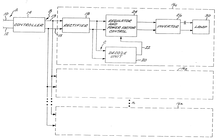
Referring now to Figure 1, a simplified block
diagram of the dimming ballast control system of the present
invention is illustrated.
In particular, standard electrical power (standard
line source, typically 120 volts AC, 60 hertz) is supplied
over power lines 10 and 12 located in a building structure to
a controller 14 (waveform A, Figure 2A) located~in a wall
switch unit. Controller 14, as set forth in more detail
204907~
hereinafter, removes (or reduces the amplitude of) one pulse
from the incoming alternating waveform in a predetermined time
period N (waveform B, Figure 2A). The time between missing
pulses corresponds to a desired lamp dimming (power) level.
The output signal from control 14 is applied to a plurality of
remote ballast units 161, 162...16n. Each ballast unit is
identical and thus only unit 161 will be described in detail.
The ballast unit 161 comprises a rectifier 18 which provides
a rectified DC voltage at its output (waveform C shown in
Figure 2A), a decoder unit 20 coupled to the output of
rectifier 18, decoder 20 providing a reference control signal
on lead 22 to IC regulator and power factor control unit 24 as
will be described in more detail hereinafter. Regulator unit
24, coupled to the output of rectifier 18, provides a
regulated DC voltage output which is adjustable. The output
signal from regulator unit 24 is coupled to invertor 26 which
provides a high frequency AC signal, the frequency of the
signal being dependent on the magnitude of the DC signal at
the invertor input. The high frequency AC signal is coupled
to ballast capacitor 28 and then to the fluorescent lamp being
controlled. The ~ ;ng ballast systems are located remotely
from the wall switch and typically adjacent the fluorescent
lamps.
An alternate encoding arrangement is represented by
the corresponding waveforms shown in Figure 2B wherein a
sequence of missing pulses corresponds to a particular dimming
level desired. The following description assumes that the
encoding system shown in Figure 2A is being utilized.
As will explained in detail hereinafter, the output
signal from the decoders determine the magnitude of the DC
applied to invertor 26 and thus the AC voltage (current)
applied to lamp 30. Invertor 26, in addition, controls the
lamp filaments in a manner such that the filament voltage
increases proportionately to the decrease (dimming) in voltage
applied across the lamps.
~04 g~ 75
In the system illustrated, the same dimming voltage
is applied to each lamp responding to controller 14.
Typically, a single wall switch in a room, for example,
controls all the lamps in that room in an identical fashion.
5Figure 3 is a schematic diagram of controller 14.
The voltage on lines 10 and 12 is applied to the primary
winding 30 of transformer T1. An auxiliary winding 32 of
transformer Tl is connected to a full wave rectifier 34, the
output thereof being coupled to pin VCC of microcomputer 36
lovia power signal conditioner circuit 35. Auxiliary winding 37
power applies the AC line signal appearing at primary winding
30 to pin T1 of microprocessor 36 in the form of periodic
input pulses. Preferably, microcomputer 36 is the Model 8048
manufactured by Intel~Corporation, Santa Clara, California.
15 Input pins Plo, PllPl5, are connected to ground via keys, or
pushbuttons, 50, 48...40, respectively, as illustrated. Keys
40, 42...48, shown in the open or inoperative position, turn
on fluorescent lamps when pressed to close the contacts and
correspond to five different lamp power settings. The keys
are located in the wall switch box. Key 50 corresponds to the
off key and when closed causes microcomputer 36 to open J2 and
turn off the lamps. As an optional device, a remote infrared
controller 54 is used to control an infrared receiver 56, the
coded output thereof being connected to ~ pin To of
microprocessor 36. As will be described with reference to the
flowchart shown in Figure 4, activation of one of the
pushbuttons 40, 42...48 generates a signal at pin P22 which
controls the magnitude of the voltage at the output of
transistor Q1, and through transformer T2, the conducting
state of thyristor, or silicon controlled rectifier, 60.
Thyristor 60 determines the time period N between missing
pulses of the coded signal (waveform C, ~igure 2A) being
transmitted to decoder unit 20.
Figure 4 illustrates the transmitter encoding flow
chart. The flow chart is set forth to enable a computer
* trade-mark
D
Z ~ 5
programmer to program the Intel microcomputer described
hereinabove in a manner such that the appropriate ~; mm ing
coded signal is produced in response to a selected key. In
particular, when the microcomputer 36 is activated (symbol
70), the microcomputer initially determines whether any one of
the keys 40, 42...48 have been engaged (symbol 72). If one of
the coding keys has been depressed, the microcomputer next
determines whether the turn-off key has been activated (symbol
74). If yes, the system is turned off (symbol 76) and the
microcomputer returned to the start position. If no turn-off
signal is present, the microcomputer 36 checks to see if relay
J2 is activated (transistor Q3 is turned on) (symbol 77). If
not, Q3 is turned on and a delay (symbol 81) is imposed to
enable the lamps to start at the highest level (intensity)
before returning to its preset level. If the microcomputer
determines that relay J2 is engaged (Q3 on), the
microprocessor 36 next searches a particular address in a
look-up table for the depressed key (symbol 78). It should be
noted that relay Jl is used to minimize energy losses during
the time periods when the remote control function is not being
utilized. When the system is used, the Jl relay contact is in
the open position. After the relay contact is in the open
position (symbol 80), thyristor 60 is used to prevent the
first pulse (waveform Figure 2A) in the AC ~signal to be
transmitted to the ballast (symbol 82). As noted above, a
register in microprocessor 36 has been set to a value
corresponding to the particular key which has been depressed
(in fact, the value in the register corresponds to the time
period N). The register (symbol 84) is decremented each time
a rectified pulse is detected at pin T1 of microcomputer 36.
If the register is not zero (symbol 86), the output at pin P22
is such that transistor Q1 causes thyristor 60 to allow the
power to be transmitted to the ballast via lines 13 and 15.
When the register is zero, the output at pin P22 causes
transistor Q1 to bias thyristor 60 in a manner to prevent the
204~7~
second pulse to be transmitted during the period N (symbol
88). The relay is then deenergized (symbol 90), closing the
relay contact. After a predetermined delay (symbol 92) to
allow for mechanical "debouncing" of the keys, the cycle
repeats itself (microprocessor 36 scans pins P1o, Pl1.... P15
continuously to ascertain whether the setting for the lamp
intensity has changed).
As noted previously, the ballast system of the
present invention is arranged to have a remote infrared
control option whereby a user can adjust the lamp dimming
without depressing a key on the wall switch box. In this
case, if the microprocessor 36 determines a key has not been
depressed (symbol 72), a determination is made if a signal is
at pin To (symbol 94). If not, the cycle is restarted. If
there is a signal present, a check is made to see if the
signal (most remote infrared signaling devices have a preset
address data) has a correct address (symbol 96). If not the
cycle is restarted. If the address is correct, a check is
made to see if the preset signal data (a portion of the entire
data) is correct (symbol 98). If not, the cycle restarts. If
the data is correct, the remaining portion of the data, coded
to correspond to one of the keys 40, 42...48 when depressed,
causes the cycle (symbol 100) to start at the input point to
symbol 74 as illustrated.
Referring now to Figure 5, a schematic diagram of the
ballast system P23 is illustrated.
The coded signal (waveform B, Figure 2A) on the power
output lines 13 and 15 (Figure 3) is coupled to the input
power lines 63 and 65, respectively, as illustrated. The
coded signal is applied to rectifier circuit 18 comprising
diode full wave bridge circuit 67 and to regulator unit 24.
The signal output from bridge circuit 67 is coupled to Schmitt
trigger circuit 71 via a voltage divider circuit comprising
resistors 73 and 75, trigger circuit 71 converting the missing
rectified AC pulse waveform to a corresponding shaped pulse
7 5
12
waveform which is applied to input pin 30 of microprocessor
120. The output of the bridge circuit 67 is also applied to
one input of integrated circuit 110. As explained
hereinafter, the output of circuit 110, preferably a
commercially available Siemens TDA 4814A chip, switches MOSFET
112 from a conducting to a non-conducting state and vice versa
at a frequency rate dependent upon the magnitude of the input
voltage, the DC bus voltage, the inductance value of the
inductor choke (114) and the desired input current. This in
turn causes energy to be transferred from inductor choke 114
to output junction 118 (and across capacitor C2). Integrated
circuit 110 also senses the input voltage waveform at pin 11
and forces the input current to resemble the voltage. As a
result, the input current and input voltage will be
substantially in phase and the power factor (cosine of the
phase angle between the waveforms) will be close to one,
typically 0.995. Thus, the harmonic content of the input
current will be greatly minimized. As noted above,
microcomputer 120, preferably an Intel~8051, functions to
decode the input coded signal and effectively generate a
resistance value at node 116 (input to pin 12 of chip 110)
corresponding to the appropriate key depressed in the wall
switch unit (it should be noted that the ballast system of the
present invention can also be utilized without remote control
i.e. if a variable resistance is-applied directly across the
taps a and b illustrated). In particular, and as explained
with reference to the flow chart shown in Figure 6,
microcomputer 120 continuously scans input pin P30 and
determines the length of time between missing pulses.
According to this information, selected ones of the open drain
inverters 124, 126...130 connected to pins P1o~ P11...P13,
respectively, are biased into the non-conducting state, thus
connecting the resistances associated therewith into a voltage
dividing circuit with resistances R120. The value of the
resistance applied to pin 12 determines the DC bus voltage at
G
~ ~ 4 ~ ~ 7 ~ ~
13
junction 118. Changing the DC bus voltage at junction 118
determines the energy transfer (pulse) rate of the signal from
inductor (choke) 114 applied across capacitor C2. It should
be noted that chip 110 and the boost converter circuit are
connected in a manner such that a total DC voltage at junction
point 118 is greater than the peak input voltage (170 volts)
applied to lines 63 and 65.
The output section of the ballast is basically a
self-resonating halfbridge invertor which converts the DC
power to high frequency AC (20-50 KHZ), the circuit comprising
capacitors C3, C4, C6, C7 and C10, transistors Ql and Q2,
transformer T103 and diodes D5, D6, D7, and resistors Rl, R2,
R3 and R4. In this invertor circuit, the output voltage
waveform is close to sinusoidal. The frequency is mainly
determined by capacitor C7, the inductance of the primary
winding of transformer T103, capacitor C10 and load (lamp)
impedance. To control the filament voltage applied to
fluorescent lamps Ll and L2 (although only two lamps are
illustrated, the concept of the present invention can be
utilized with one or more than two fluorescent lamps), a
transformer T104 which is a ferrite core is utilized.
Increasing filament voltage during dimming is accomplished by
saturable transformer T104 which is connected in series with
the secondary winding of T103 and capacitor C7, a resonant
tank with reasonably higher impedance than the input impedance
of T104. The filament voltage is determined by the number of
turns wound on the ferrite core and the frequency of the
resonating circuit. Transformer 104 is designed to operate at
deep saturation when maximum voltage appears across C2. As
the output voltage across C2 is reduced, for example, by the
control of microcomputer 120, the frequency of the resonating
circuit will increase as the impedance of the fluorescent
lamps increase. Thus, the voltage over the filaments of the
lamps will increase accordingly, both stabilizing the lamp
light output when dimmed down and increasing lamp life.
The operating points of the fluorescent lamps in the
2049075
preferred embodiment are set substantially as follows:
Liqht Output Lamp Voltage Resonant Frequency Filament Voltage
~ Watts (Volts) (KHz) (Volts)
100% 230 420 20.04 3.54
75% 172 336 20.62 3.72
50% 115 267 22.10 3.94
25% 57.5 237.5 24.57 4.095
10% 23 220 25.55 4.072
The details of the circuit operation are as follows. The
voltage output from the secondary winding of T104 is applied
across lamps Ll and L2. The inductor (choke) T102 limits
current flow in the circuit, thus enabling a sinusoidal
waveform to be generated. The voltage across windings T103
and T104 also have a sinusoidal waveshape, winding T104 being
coupled to the lamp filament windings, the secondary winding
of T103 being coupled across the lamp to initiate the arc.
Windings T103 and T104 and a capacitor C7 form the circuit
resonant tank. Winding T104 is designed to make the core
2Q saturate, the secondary voltage from T104 being substantially
constant because its flux density is set to the maximum. The
nominal (highest level) DC bus voltage at junction point 118,
for 100% light output, is set at 420 volts. When the DC
voltage at junction point 118 is reduced, the voltage of the
secondary winding of T103 is also reduced proportionately.
Thus the current through C10 and the lamps Ll and L2 is also
reduced. Since each lamp has a negative resistance, as
current is reduced, the voltage increases and the lamp
impedance increases. The effective capacitance of C10
reflected to the primary of T103 is reduced, the overall
circuit reactance thus being lower and increasing the circuit
resonant frequency. Since the core of T104 is in deep
saturation, the voltage reduction does not change its status,
the flux density remaining substantially constant. In this
case, the voltage applied to the lamp filaments is essentially
7 5 ~
proportional to the resonant frequency. The above operation
repeats itself as the dimming voltage decreases.
Resistances R100 and R101 sample the sinusoidal
input voltage waveform to the circuit, or chip 110, to control
the power correction factor. It is, as noted hereinabove,
preferred to have the input current close to the input voltage
(phase, shape). The input current is sensed as it flows
through resistors R107 and R108. Resistors R105 and R106 are
used to compensate for the voltage of the fluorescent lamps
being used. Capacitor C108, resistor R120 and the effective
variable resistance at node point 116 functions both to filter
out 120 Hz ripple and as a voltage control loop, i.e. to
stabilize and regulate the DC voltage at node point 118.
Figure 6 illustrates the receiver decoding flow chart. The
flow chart is set forth to enable a computer programmer to
TY
program the Intel No. 8051 microcomputer described hereinabove
in a manner such that the D.C. voltage corresponding to the
desired lamp output dimming is provided to the circuitry
controlling lamp operation.
At the start of the operation of microcomputer 120
(Figure 5), register Ro is set to zero (symbol 152) and the
input to microcomputer 120 from the Schmitt triggers is tested
(checked) continuously (symbol 154). The input testing is
done on a continual basis. If the initiai input test
indicates that an input pulse is not present, the Ro register
is incremented one unit (symbol 156). If the input test
indicates a pulse is present, the process restarts. The input
is tested again (symbol 158) and if no input pulse is present,
the Ro register is incremented one unit. If the input test
indicates that a pulse is present, the count in the Ro
register is compared with the value in the PULSE register
(symbol 160). The PULSE register has a value corresponding to
the time period of a missing pulse. If the value in the Ro
register corresponds to the value in the PULSE register
(corresponding to the first pulse after a period during which
, .,
~.,~'
2~49075
16
no pulse appeared) a third register (CODE) is tested to
ascertain if it is set to 1 (symbol 162). If not, the CODE
register is set to 1, the timer is first cleared and then
started (symbol 164). If the CODE register previously has
been set to 1, the value in the timer is transferred to an
accumulator, the value in the accumulator corresponding to an
address in a look-up table (symbol 166). The value in the
look-up table corresponds to the key depressed in the wall
switch box. If the value in the timer is not the preset value
(symbol 168), the time value will not be decoded, the CODE
register is cleared and the timer is stopped (symbol 172) and
the process restarted. If the value in the timer is correct,
a control code corresponding to the key depressed in the wall
switch box can be obtained from the look-up table. The
control code is sent to pins P1o through P1s to control the
corresponding pin (symbol 170). In this case, the CODE
register is cleared, the timer stopped and the process
restarted.
The present invention thus provides an improved
dimmable fluorescent lamp ballast system which encodes the
power line signal in a building structure in accordance with
a desired dimming state such that additional wires are not
required in the structure, thereby reducing the cost of system
installation. In addition, the lamp filament voltage is
maintained substantially constant or increased slightly as the
dimming voltage is decreased, thus both stabilizing lamp light
output and prolonging lamp life.
The concept of providing a building structure
control system for controlling the operating status of a
remote device, as set forth in the present invention, without
adding additional wires to the structure, can be utilized to
control devices other than fluorescent lamp ballasts, such as
other gas discharge lamp systems, air conditioners, and
dampers.
20~9075
While the invention has been described with
reference to its preferred embodiment, it will be understood
by those skilled in the art that various changes may be made
and equivalents may be substituted for elements thereof
without departing from the true spirit and scope of the
invention. In addition, many modifications may be made to
adapt a particular situation or material to the teaching of
the invention without departing from its essential teachings.