Note: Descriptions are shown in the official language in which they were submitted.
W0 9ltll852 ~ ~) PCr/US91/00511 `
~ .,
- 1 - .
FAST~SWITCHING FREQUENCY SYNTHESIZER
:,~
Technical Field j`
This application relates to frequency synthesizers and more
particularly to fast-switching frequency synthesizers. `~
~
Background of the Invention
It is common to use a single frequency synthesizer in an FM radio `
to generate both the transmit frequency source and the receive local
oscillator ("LO") for down-conversion. This type of synthesizer is typical -in applications where a device receives and transmits on the same
channel at different points in time. A significant problem in this type of
application is getting the synthesizer to switch between the transmit
frequency and the receive LO frequency as quickly as possible. The time ~`
the synthesizer takes getting between these two frequencies is literally
wasted by the radio since it can neither transmit or receive during this
time period.
Some past approaches to reducing this switching time have
26 included, for example, parameter optimization and adaptive filtering.
Each of these approaches, however, has limitations. A problem with
WO 91/11852 ~ 4 ~ PCI'/US91/00511 ` .
parameter optimization has been that it requires modifying the closed- `
loop bandwidth. A problem with adaptive filtering has been transients
and loop response optimization.
As a result, there is a need for an improved fast-switching
5 frequency synthesizer.
, ~
Summary of 1he invention
Therefore, an improved fast-switching frequency synthesizer is ;
provided. According to the invention, the synthesizer utilizes presteering
voltage injection at the voltage controlled oscilla~or ("VCO~') to cause the ~
frequency to change rapidly. Also, feedback is added to the presteering `
network to maintain an accurate presteering voltage as the gain of the
VCO varies from unit to unit or drifts with temperature and age. The ~
improved fast-switching frequency synthesizer, according to the ` `
invention, also uses the presteering voltage value to control the '~''!
transmitter deviation, thereby eliminating the need for manual alignment.
Brief Desc~ Q.n. ~o~f lh~ D~ Qg~
Fig. 1 is a block diagram that shows a first embodiment of an
20 improved fast-switching frequency synthesizer 100, according to the
invention.
Fig. 2 shows the frequency pre-steering and deviation control
circuit 200 ot the first embodiment. ;
Fig. 3 shows a flow diagram 300 for the first embodiment.
petailed Descri~tion ot the Invention
WO 91/11852 2 0 ~1 ~ 3 ~ 6 PCI'/US91/00511
. ~
-3-
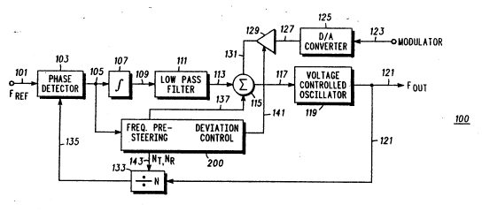
Fig. 1 is a block diagram that shows a first embodiment of an -`~
improved fast-switching frequency synthesizer 100, according to the
invention. As shown, the synth~siz~r is arranged with a frequency~pre- ~ .steering and deviation control circuit 200. The synthesizer has two inputs
5 -- a reference fraquency signal 101 (fret) and a digital baseband
modulator signal 123.
As shown, the frequency reference signal 101 is input to the
phase/frequency detector 103 where it is compared to the divided-down
VCO output frequency 135. An output error signal 105 of the phase
detector 103 is next applied to integrator 107. This integrator 107 is a ``
typical integrator unit with a response in the S-plane of (s+a)/Ks.
The integrator output 109 is next applied to the low pass filter 111.
This filter may be, for example, a typical 3-pole design with a bandwidth
at least one order of magnitude greater than the natural frequency of the
15 closed loop transfer function and at least one octave (preferably one
decade) in frequency less than fret (101).
As shown, the digital baseband modulator signal 123 is input to
the digital to analog (D/A) converter 125 to provide an analog baseband
modulator signal 127. This signal is then-level-adjusted by a variable
gain device 129 to set the FM deviation. The gain of device 129 is ~
adjusted by level control line 141. --;
Returning now to low pass filter 111, the filte~s output 113 is
summed with the analog baseband modulator signal 131 and signal 137
by the summing amplifier 115. The summing amplifier's output 117 is
2~ then input to the control line of the voltage controlled oscillator (VCO)
1 19. The output of the VCO 1 19 is the transmitter RF frequency output
wo gl/11852 P(:~/uS91/005~
~ U Ll ~ 6
-4-
signal 121. This signal is divided down to a frequency 135 equal to the
frequency of fref 101 by the divider 133's divisor (N). As shown, N is
controll~d by lead 143, and altemates between two values -- Nt -
corresponding to the transmit frequency and Nr corresponding to the
5 receive LO frequency.
As shown, the frequency presteering and deviation control circuit
200 switches the synthesizer 100 between the transmit frequency and
the receive local oscillator (LO) frequency by changing the value of N via
lead 143. As will be seen below, the circuit 200 also encourages the
10 synthesizers fast transition between states by simultaneously applying a
voltage step signal of optimum amplitude to the VCO 119 via lead 137.
When the sy~thesizer goes to the transmit state, the frequency
presteering and deviation control circuit 200 changes signal 143 from Nr
to Nt simultaneously while injecting a positive^going voltage step signal
15 at lead 137 to cause a corresponding change in voltage at the VCO input
117. As will be seen, the amplitude of this step signal has been
determined to be the optimum value to change the VCO frequency from
receive LO to transmit frequency. As a result, frequency changes at lead
135 are minimized and thus the error voltage 105 remains generally
20 constant.
When the synthesizer goes to the receive state, the frequency
presteering and deviation control circuit 200 changes signal 143 from Nt
to Nr simultaneously as it changes the voltage at 137 from the above
positive value back to zero. This negative-going voltage step at 137
25 causes a negative-going step at 117. As above, this voltage is
'.
. :.
~ j .
WO 91/118~2 ~ O L~ 9 ~ (~ 6 PCI`/US9~/00511
- 5- ``-
substantially the voltage needed to change the VCO frequency from
transmit frequency to receive LO frequency.
One problem with this pre-steering voltage arrangement 7s that the ~ `
optimum value of step voltage change at the VCO input 1 17 to cause the
- 5 frequency transition varies with temperature changes and unit variations.
This is primarily due to variations in the voltage-versus-frequency
characteristic of the VCO.
To solve this problem, the phass detector output signal 105 is ~`
used as an input to the frequency presteering and deviation control
circuit 200 to provide feedback to keep the amplitude of the voltage step
at lead 117 as close to the optimum value as possible. This is explained
below.
Ideally, the phase detector 103's output signal 105 should be ;
constant with zero slope at all times. According to the invention, circuit
200 incrementally increases`or decreases the size of the voltage step
137 based on the slope of signal 105. This process is repeated each
time the synthesizer switches from the transmit to the receive state. This -
adjustment continues until the slope of signal 105 is substantially zero ,
and the step voltage 137 reaches its optimum value.
Moreover, the inventor has discovered the voltage step on signal
137 also gives a reîative indication as to the slope variation in the VCO
frequency-versus-voltage curve. Since the deviation of the FM
transmitter also depends on the slope of this VCO curve, this indication
may be used to adjust the relative FM deviation corresponding to that
curve. According to the invention, the frequency presteering and
deviation control circuit 200 uses level control signal 141 to control the
wo 9l~ll8s2 ~ o ~ ~ 3 i ~ PCItUS91/00511 ,
. .
-6-
variable gain device 129 in the baseband modulator path. Thus, when ;
circuit 200 determines that the gain of the VCO has increased (or
decreased), it decreases (or increases) the gain of device 129 via signal
141 to maintain a constant FM dsviation.
Referring now to Fig. 2, there is shown the frequency pre-steering
and control circuit 200. As shown, signal 105 is applied to a low pass
fîlter 145. Filter 145 should have a bandwidth of at least twice that of the
closed loop natural frequency of the synthesizer loop. The filter's output
147 is applied to slope detector 149. Slope detector 149 may be
implemented, for example, by an A/D converter that samples two points
in time and then compares them. Alternatively, detector 149 may be
implemented by a comparator having signal 147 as a first input and a -
band-limited version of signal 147 as a second input. As shown, slope
- detehor 1 49's output (151 ) is coupled to logic circuit t 53.
As depicted, the logic circuit 153 receives the slope measurement
inforrnation via signal 151.
The logic circuit 153 has four outputs -- the divisor output signal
143, a selector control path 161, a latch control path 179, and an
- ~ up/down countercontrol path 175. ;
The up/down counter output 177 is periodically transmitted to latch
173 under control of control path 179. As will be seen, the latch output
bus 139 is used to generate both the level control signal 141 and the ;;
step voltage signal 137. The number of output bits in the up/dowh
counter 171 should at lQast be the same as the number of bits on the
latch output bus 139. Alternatively, the up/down counter 171 may have
more bits than the bus 139 if the additional bits of the counter 171 are
,
WO 91/11852 2 0 L~ 9 3 4 ~ PCI`/US91/00511
below the least significant bit of the bus 139. This configuration would -:
effectively create a time constant in the counter 171 so that it would take
more than one increment (or decrement) in a row to toggle the least
significant bit of the bus 139. The process of incrementing,
decremanting, and latching the up/down counter 171 will be discussed
below.
As shown, the level control signal 141 is generated by applying
the latch output bus 139 to the input of digital to analog convertsr 169.
The output of converter 169 is the level control signal 141.
As shown, the step voltage signal 137 is generated by alternately
switching selector 163 between it's "A" input 155 and it's "B" input 157.
Latch ouSput bus 139 is applied to the A input 1~5, while all zeroes --
represented by the ground signal 159 -- is applied to the B input 157.
The logic circuit 153 selectively toggles the selector 163 between the A ~.
and B inputs via control lead 161. The selector output 165 is applied to
the input of digital to analog converter 167. The output of converter 167
is the step voltage signal 137.
Flg. 3 shows a flow diagram executed by the logic circuit 153. The
process starts at step 301, and then goes to step 303. Here the process
waits for a request for the synthesizer to go to the transmit state. When
the synthesizer is ready to go to the transmit state, the process goes to `
step 305.
In step 305 selector control lead 161 switches the selector 163
output 165 from the ground signal l S9 present on the B input (157~ to the
latch output bus signal 139 present on the A input ~155), thereby injecting
the presteering voltage step signal via step voltage output 137. Also in
WO 91/118!;2 2 t~ ~ 9 3 ~ ~ PCI`/US91/0051.1
,..
- 8 - ~ -
this step, divisor output lead 143 switches divider 133 from the N~ divisor
to the Nt divisor. As a result of these actions, the synthesizer switches . ;
from the receive LO frequency to the transmit frequency.
The process next goes to wait step 307. The process waits here
5 for a time period approximately 2 times the time constant of the
synthesizer's closed loop transfer function. The time delay here allows
the phas~ detector 103 to possibly generate an error signal in the event
the step voltage level 137 is not at it's optimum value.
The process next goes step 309 where the slope measure of ~
1 0 phase detector output 105 is taken from signal line 151. ~;
The process next goes to decision step 311 where it determines ^
whether the s.ope measurement of phase detector output 105 is positive
or negative. It the slope is positive, the process goes to step 313, where ;~
it increments (steps up) the up/down counter 171. If the slope is
negative, the~process goes to step 315, where it decrements (steps
down) the counter 171.
The process nex~t goes to step 3t 7 where it waits for a request for ij
the synthesizer to go to the rèceive state. When the synthesizer is read~ -`
to go to the receive state, the process goes to step 319.
~ In step 319 selector control lead 161 switches the selector 163
output 165 from the latch output bus signal 139 present on the A input
(155) to the ground signal 159 pr~sent on the B input (157), thereby
removing the presteering voltage step signal via step voltage output 137~ -
Also in this st~p, divisor output lead 143 switches divider 133 from the Nt
divisor to the Nr divisor. As a result of these actions, the synthesizer
swlitches from the transmit frequency to the receive LO frequency.
' ','
WO 91/11852 2 0 ~ ~ 3 ~ ~ PCI'/US91/00~11
The process next goes to step 321, which is a wait step
functionally equivalent to that of step 307 (see above).
The process next goes to step 323, which is a slope measurement
step functionally equivalent to that of step 309 (see above).
S The process next goes to decision step 325 where it determines
whether the slope measurement of phase detector output 105 is positive
or negative. If the slope is positive, the process goes to step 327, where
it decrements the up/down counter 171. If the slope is negative, the ;
process goes to step 329, where it increments the counter 171.
The process next goes to step 331. This step 331 latches the ~.
up/down counter output 177 onto bus 139. The process now returns ;
(step 333) to step 301.
,; ~".
Those skilled in the art will appreciate that logic unit 153 may be
implemented, for example, by a suitably-programmed microprocessor
together with necessary IQ9jC circuitry and units. Also, it will be apparent
to those skilled in the art that the up/down counter 171 may be
incremented and/or decremented by any convenient predetermined
valuè such as, for instance, by the value 1.
As mentioned above, a significant problem in radio manufacturing
today is the effort required to calibrate the transmitter deviation. Manual
techniques are especially undesirable here since they both reduce
reliability and increase cost.
The present invention is particularly beneficial in this area since it
allows the transmitter deviation to be adjusted and maintained `
WO 91/11852 ~ O ~ g 3 ~ ~ PCr/US91/0051.1
,......... ..
- 10- ~
`::
automatically, thereby eliminating manual alignment during production,
while adding only a small amount of extra circuitry. In fact, the over-all
cost of such units might even be reduced somewhat since the àutomatic ~ `
adjustment feature allows components with more coarse and/or less - .
precise tolerances to be used in production. Moreover, as discussed
above, the invention also helps to guarantee that the alignment will re- ;`
adjust itself to the optimum value during the lifetime of the finished unit, `
by automatically compensating for the effects of heat and aging. As a
result, the unit's over-all reliability and useful life-span have also been `
significantly increased.
Still another benefit of the present invention is it also corrects for
variations in deviation that might be caused by channel changes due to
VCO gain changes for varying and differing channels.
Another benefit of the invention, of course, is that it enables a radio ,'`'~!
1~ transceiver using such a synthesizer to switch from a transmit to a receive
state in the minimum time. This quick switching -- or "turnaround" -- time -~-
from transmit to receive could be very beneficial, for example, in a data `
application wher~ a host computer is polling a large number of data
terminals in a round-robin pattern via a common radio link. The
switching time of each radio-terminal would be critical here since each ~;
terminal must normally reside in the receive mode to determine when it is
being polled -- or ~addressed" -- by the host. Once a terminal is polled, it
must then switch to the transmit mode before it can transmit it's data to ``
the host. As a result, the time required for the host to poll all the terminals
on the radio link will be limited by the ma!hematical sum of the individual ;
switching tim~s for all the terminals. Thus, for a large number of
.~
WO 91/11~52 ~ 'j PCr/US91/00511
- 1 1 -
terminals, even a relatively small decrease in the transceiver switching
time of each radio could result in a substantial increase in efficiency and
data through-put for the host computer. ~ ~
While various embodiments of a fast-switching frequency ~`
synthesizer, according to the present invention, have been described
hereinabove, the scope of the invention is defined by the following
claims. .
.:
' ~