Note: Descriptions are shown in the official language in which they were submitted.
20 ~ 9~
1 BACKGROUND OF THE INVENTION
The present invention relates to an
asynchronous transfer mode (ATM) switch in which
information switching is accomplished in a unit of cells
or to an ATM switch and a method of controlling the same
in an ATM cross-connection system.
In an ATM switch of the prior art, each ATM
cell is assigned with a routing tag so as to be routed
depending on the routing tag.
As stiplulated in the CCITT Recommendation
1.432, an ATM cell is 53 bytes long. In operation inside
the ATM switch, a routing tag is added thereto such that
an ATM cell in the switch includes 54 to 64 bytes. The
ATM cell has a period or cycle of about 44 cells for each
125 microseconds (~s) in a 150 Mb/s operation. For
example, an ATM switch processing about 2800 cells in
each 125 ~s (equivalent to 150 Mb/s x 64 lines) has a
switching capacity of about 10 Gb/s. In this conven-
tional technology, when configuring an ATM switch of such
a large capacity, a plurality of unitary switch LSIs are
arranged in a two-dimensional structure. Such an ATM
switch has been described, for example, in an article
"Development of ATM Switch LSIs for Broadband ISDN"
written by J. Kamoi et al. in the Proceedings of 1990
Spring Convention of IEICE of Japan, B-443 (March 18,
&
1 1990), p. 3-21. Specifically, 64 one-chip LSIs each
including an 8 x 8 switch (150 Mb/s) are arranged in a
two-dimensional constitution to construct a 64 x 64
switch (150 Mb/s).
In the ATM switch of the prior art, since each
ATM cell is routed by use of a routing tag assigned
thereto, the ATM cell is switched together with the
routing tag in any situation. Consequently, the switch-
ing capacity of the unitary ATM switch is restricted by
the size of a hardware system of the switch to be mounted
in a one-chip LSI and the signal capacity i.e. the
maximum number of input/output signals to be processed by
the one-chip LSI. In order to improve the performance of
the switch, the unitary switches are required to be
configured in a two-dimensional form as described above.
However, this is attended with a problem that the
hardware size increases in proportion to a square of the
switch capacity.
Meanwhile, JP-A-2-2767 (laid-open on Jan. 8,
1990) corresponding to DE-A-3742941 shows a packet switch
system having input devices, one provided between a
switch and each of inputs, in which the input devices
serve to divide packets into sub-packets.
SUMMARY OF THE INVENTION
It is therefore an object of the present
invention to provide an ATM switch which can be
implemented with a hardware system having a small size
2049366
even when the switching capacity is increased.
In accordance with one aspect of the invention there
is provided an ATM switch comprising: cell partitioning
circuits each for subdividing an ATM cell into N partial
cells, where N is an integer greater than 1, and for assigning
an identical routing tag to the obtained partial cells; and
N partial cell switches each for receiving each partial cell
of the N partial cells from said cell partitioning circuits
and for routing said received partial cell based on the
routing tag attached to the partial cell without any routing
control information from other partial cell switches.
In accordance with another aspect of the invention
there is provided an ATM switch control method of controlling
an ATM switch including error correcting code (ECC) encoder
circuits each for generating, for an ATM cell as an
information field of an ECC, ECC check symbols and for adding
the ECC check symbols thereto, cell partitioning circuits each
for subdividing said ATM cell into N partial cells, where N is
an integer greater than 1, for subdividing said check symbols
into M partial cells, where M is an integer greater than 1,
and for assigning an identical routing tag to the obtained
(N+M) partial cells, (N+M) partial cell switches each for
receiving each partial cell of the (N+M) partial cells from
said cell partitioning circuits and for routing said received
partial cell based on the routing tag attached to the partial
cell without any routing control information from other
partial cell switches; and ECC decoder circuits for receiving
the (N+M) partial cells thus routed from said (N+M) partial
204q365
cell switches and for achieving an error correction on the
received partial cells comprising the steps of: detecting a
frequency of error correction or detection in either one of
said ECC decoder circuits; deciding whether said frequency is
not below a preset frequency; and resetting said (N+M) partial
cell switches.
The total switching capacity of the ATM switch is
obtained by multiplying the capacity of the unitary partial
cell switch by the cell partitioning value of the number of
the total partition cells; consequently, there can be
configured a unitary ATM switch having a remarkably large
capacity by increasing the cell partitioning value.
The foregoing and other objects, advantages, manner
of operation, and novel features of the present invention will
be understood from the following detailed description when
read in connection with the accompanying drawings.
BRIEF DESCRIPTION OF THE DRAWINGS
Fig. 1 is a schematic block diagram showing the
constitution of an ATM switch in a first embodiment according
to the present invention.
Fig. 2 is a diagram showing the structure of ATM
cells used in the first embodiment according to the
- 3a -
. . ~
2 ~
1 present invention.
Fig. 3 is a schematic diagram showing the
structure of partial cells employed in the first
embodiment according to the present invention.
Fig. 4 is a block diagram illustratively
showing the constitution of an ATM switch in a second
embodiment according to the present invention.
Fig. 5 is a schematic diagram showing the
structure of partial cells employed in the second embodi-
ment according to the present invention.
Fig. 6 is a block diagram schematically showing
the configuration of an ATM switch in a third embodiment
according to the present invention.
Fig. 7 is a schematic diagram showing the
structure of partial cells employed in the third
embodiment according to the present invention.
Fig. 8 is a block diagram illustratively
showing the configuration of an ATM switch in a fourth
embodiment according to the present invention.
Fig. 9 is a schematic diagram showing the
structure of partial cells employed in the fourth
embodiment according to the present invention.
DESCRIPTION OF THE PREFERRED EMBODIMENTS
Referring now to Fig. 1, a description will be
given of a first embodiment according to the present
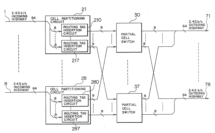
invention. The configuration of an ATM switch of Fig. 1
includes 2.4 Gb/s incoming highways 1 to 8, cell
2 ~
1 partitioning circuits 21 to 28, partial cell switches 30
to 37, and 2.4 Gb/s outgoing highways 71 to 78. The cell
partitioning circuits 21 to 28 respectively include
routing tag insertion circuits 210 to 217, 220 to 227,
..., and 280 to 287.
Next, the operation of the first embodiment
will be described. Each of the 2.4 Gb/s incoming
highways 1 to 8 is disposed to receive a 56-byte ATM cell
in a format of "40 Mb/s x 64 bits in parallel x 7 rows"
as shown in Fig. 2. The ATM cell includes an 8-byte cell
header and 48-byte cell information field. Each of the
cell partitioning circuits 21 to 28 subdivids the cell
in the form at N40 Mb/s x 64 bits in parallel x 7 rows"
into eight portions including eight bits in parallel and
assign an identical routing tag thereto, thereby obtain-
ing eight partial cells 150 to 157 as shown in Fig. 3.
These partial cells are then sent to the different
partial switches respectively associated therewith. For
example, in the cell partitioning circuit 21, the routing
tag insertion circuit 210 outputs a 0-th partial cell 150
to the partial cell switch 30 and the routing tag
insertion circuit 211 supplies a first partial cell 151
to the partial cell switch 31. In the partial cell
switch 30, 0-th partial cells are received respectively
from the cell partitioning circuits 21 to 28 so as to
achieve a switching operation on the received 0-th
partial cells based on the routing tags respectively
assigned thereto. In the similar manner, the partial
~ 2049366
1 cell switches 31 to 37 conduct switching operations
respectively of the first to seventh partial cells.
Since the partial cells created from a cell are assigned
with an identical routing tag, all partial cell switches
30 to 37 accomplish a similar switching operation when
the circuit system operates in the normal state. In
consequence, the 2.4 Gb/s outgoing highways 71 to 78
simultaneously receive the respective partial cells
constituting the cell.
Next, description will be given of a second
embodiment by referring to Fig. 4. An ATM switch of Fig.
4 includes 2.4 Gb/s incoming highways 1 to 8, error
correcting code (ECC) coder circuits 11 to 18, cell
partitioning circuits 21 to 28, partial cell switches 30
to 39, ECC decoder circuits 51 to 58, error counters 61
to 68, and 2.4 Gb/s outgoing highways 71 to 78. The cell
partitioning circuits 21 to 28 comprise routing tag
insertion circuits 210 to 219, 220 to 229, ..., 280 to
289, respectively.
The operation of the second embodiment will now
be described. Via the 2.4 Gb/s incoming highways 1 to 8,
there is supplied a 56-byte ATM cell in the format of "40
Mb/s x 64 bits in parallel x 7 rows". The ECC coder
circuits 11 to 18 simultaneously receive 64 bits to
generate an ECC based on a l-byte error correcting
Read-Solomon code on a Galois field GF(28). The ECC is
a shortened Reed-Solomon code created from a generator
polynomial
-- 6
~A
G(X) = (X = ~) (X + a2)
1 where, the code length is ten bytes, the information
length is eight bytes, the check symbol length is two
bytes, the minimum distance is three bytes, and a is a
primitive element of the Galois field GF(23). Each of
the ECC coder circuits 11 to 18 accomplishes a computa-
tion by the generator polynomial to produce a two-byte
check symbol; moreover, the cell received from the
pertinent highway is transformed into a format of "40
Mb/s x 80 bits in parallel x 7 rows" to be sent to the
associated cell partitioning circuit. On receiving the
cell, the cell partitioning circuit subdivides the cell
in the format of "40 Mb/s x 80 bits in parallel x 7 rows"
into ten items associated with each eight bits in
parallel to assign an identical routing tag to the
resultant items, thereby converting the cell into ten
partial cells 160 to 169 in the format as shown in Fig.
5. The 0-th to seventh partial cells 160 to 167 are
attained by inserting a routing tag into the items
resultant from the cell partitioning operation. The
eighth partial cell 168 and the ninth partial cell 169
are created by adding routing tags to the check symbols
of the ECCs, respectively. The partial cells are
thereafter transmitted to the different partial cell
switches 30 to 39 respectively related thereto. For
example, in the cell partitioning circuit 21, the routing
2049366
'.,.~
1 insertion circuit 210 generates a 0-th partial cell 160
to be sent to the partial cell switch 30 and the routing
tag insertion circuit 211 produces a first partial cell
161 to be fed to the partial cell switch 31. On
receiving the 0-th partial cells respectively from the
cell partitioning circuits 21 to 28, the partial cell
switch 30 accomplishes a switching operation of the 0-th
partial cells depending on the routing tags respectively
assigned thereto, thereby delivering the 0-th partial
cells to the ECC decoder circuit associated with a
highway of an output destination thereof. In the similar
fashion, the partial cell switches 31 to 39 carry out
switching operations of the first to ninth partial cells,
respectively. All partial cells constituting a cell have
an identical routing tag and hence all partial cell
switches perform a similar switching operation when the
circuit system develops a normal operation. In
consequence, the ECC decoder circuit simultaneously
receives the partial cells created from the cell. For
example, the ECC decoder circuit 51 is supplied with the
0-th to ninth partial cells respectively from the partial
cell switches 30 to 39 so as to reconstruct a cell in the
form of"40 Mb/s x 80 bits in parallel x 7 rows", thereby
achieving a computation to decode an ECC of the Reed-
Solomon code for each row. When the partial cellswitches 30 to 39 normally achieve operations thereof,
the partial cells generated from a cell are simultaneous-
ly inputted to the ECC decoder circuit and there does not
2 0 ~
1 accordingly occur any error. Consequently, the error
correction is not actually conducted. However, for
example, if an error takes place in a routing tag of one
of the ten partial cells produced from a cell, even when
the nine other cells correctly arrive at the ECC decoder
circuit 51, the partial cell related to the error may not
be appropriately routined and hence cannot be received by
the circuit 51 at an appropriate time. In this case,
since the ECC system develops a function to correct a
one-byte error, the ECC decoding operation is accom-
plished with the nine correct partial cells to restore
the content of the cell not having appropriately
received. Each of the partial cell switches 30 to 39
includes a first-in first-out (FIFO) buffer, which is
disposed to temporarily store a partial cell at an
occurrence of a collision between partial cells.
Consequently, once a wrong operation occurs due to an
error of a routing tag, the order of partial cells
registered to a queue in the first-in first-out buffer of
the partial cell switch associated with the wrong
operation may possibly be different from the order of the
partial cells in a queue of any other partial cell switch
in some cases. The discrepancy between the orders of
partial cells in the respective queues results in that
any pertinent partial cell thereafter arrives at the ECC
decoder circuit 51 at a point of time different from that
of the nine other partial cells. In this situation, the
ECC decoder circuit 51 continuously achieves, for the
1 partinent partial cell, a restoration of the content
thereof through the one-byte error correction based on
the nine partial cells received at the proper time. The
discrepancy between the partial cell orders in the queues
of the FIFO buffers respectively of the partial cell
switches above is removed when the length of the queue in
the FIFO buffer of the pertinent partial cell switch
becomes zero. However, in order to cope with a case
where the queue length does not become to zero for a long
period of time i.e. where the discrepancy between the
partial cell orders in the queues is not removed for a
long period of time, the error counter 61 counts the
number of error corrections per unitary period of time.
When the count value is equal to or more than a predeter-
mined value and this condition is kept continued for aperiod of time exceeding the preset period of time, the
queue in each pertinent partial cell switch is reset. In
a case where the partial cell switches are configured to
be related to buffers respectively associated with
outgoing highways, the system resets only the buffers of
an outgoing highway associated with the condition above.
The ECC decoder circuits 52 to 58 and the error counters
62 to 68 also conduct operations in the same way as
described in conjunction wlth the ECC decoder circuit 51
and the error counter 61, respectively.
In the second embodiment, the error correction
code is used to prevent an error due to a wrong operation
of a partial cell switch from propagating to subsequent
-- 10 --
6 &
1 cells, which resultantly leads to an effect that the
wrong operation of a partial cell switch hardly causes an
ATM cell to be discarded.
Subsequently, referring to Fig. 6, a descrip-
tion will be given of a third embodiment according to the
present invention. The configuration of an ATM switch of
Fig. 6 includes Z.4 Gb/s incoming highways 1 to 8, parity
generation circuits 81 to 88, cell partitioning circuits
21 to 28, partial cell switches 30 to 37, parity check
circuits 101 to 108, error counters 61 to 68, and 2.4
Gb/s outgoing highways 71 to 78. The cell partitioning
circuits 21 to 28 respectively comprise routing tag
insertion circuits 210 to 218, 220 to 228, ..., and 280
to 288.
Next, the operation of the third embodiment
will be described. Each of the 2.4 Gb/s incoming
highways 1 to 8 is employed to supply a 56-byte ATM cell
in a format of "40 Mb/s x 64 bits in parallel x 7 rows~
as shown in Fig. 2. On receiving 64 bits in parallel,
each of the parity generation circuits 81 to 88 generates
and adds an eight-bit parity code to the received data in
a bit-parallel fashion. In the parity byte configura-
tion, an n-th bit of the parity byte (n = 1 to 8) is an
odd parity for the n-th bit of each byte in an associated
row of the ATM cell. Each of the cell partitioning
circuits 21 to 28 subdivides the cell thus including the
odd parity bits in the form of "40 Mb/s x 72 bits in
parallel x 7 rows" into nine items including eight bits
-- 11 --
1 in parallel and assign an identical routing tag thereto,
thereby obtaining nine partial cells 170 to 178 as shown
in Fig. 7. The 0-th to seventh partial cells 170 to 177
are obtained by inserting a routing tag into the items
created from the cell partitioning operation. The eighth
partial cell 178 is generated by adding routing tags to
the parity byte. Like in the first and second embodi-
ments, the partial cells are then transmitted to the
different partial cell switches 30 to 38 respectively
related thereto. On receiving the 0-th to eighth partial
cells, the partial cell switches 30 to 38 accomplish a
switching operation of these cells so as to send the
cells to the parity check circuits 101 to 108,
respectively. All partial cells resultant from a cell
are assigned with an identical routing tag and hence the
parity check circuit 101 simultaneously receives the
partial cells created from the cell when the switches 30
to 38 are operating in the normal state. However, as
described in conjunction with the second embodiment, to
cope with a wrong operation which may take place in the
partial cell switch 30, the error counter 61 counts the
number of error detections per unitary period of time.
When the count value is equal to or more than a predeter-
mined value and this condition is kept continued for a
period of time exceeding the present period of time, the
queue in each pertinent partial cell switch is reset.
When the partial cell switch is constructed to be related
to a buffer associated with an outgoing highway, the
2Q''5 f~
1 system resets only the buffers of a pertinent outgoing
highway. The parity check circuits 102 to 108 and the
error counters 62 to 68 also achieve operations in the
same fashion as described in conjunction with the
operations of the parity check circuit 101 and the error
counter 61, respectively.
Since the system of the third embodiment
detects a wrong operation taking place in any one of the
partial switches based on the partly check, even at an
occurrence of such an erroneous operation, the system can
be rapidly restored to the normal state.
Subsequently, a description will be given of a
fourth embodiment according to the present invention.
The structure of an ATM switch of Fig. 8 includes 2.4
Gb/s incoming highways 1 to 8, cell partitioning circuits
41 to 48, partial cell switches 30 to 37, sequential
number check circuits 131 to 138, error counters 61 to
68, and 2.4 Gb/s outgoing highways 71 to 78. The cell
partitioning circuits 41 to 48 are constituted with
routing tag and sequential number insertion circuits 310
to 318, 320 to 328, ..., and 380 to 388, respectively.
A description will next be given of the
operation of the fourth embodiment. Each of the 2.4 Gb/s
incoming highways 1 to 8 is employed to deliver a 56-byte
ATM cell in a format of "40 Mb/s x 64 bits in parallel x
7 rows" as shown in Fig. 2. When 64 bits are received in
parallel, each of the cell partitioning circuits 41 to 48
subdivides the cell in the form of "40 Mb/s x 64 bits in
- 13 -
2 ~_; ". t ' ~ ' t~,,
1 parallel x 7 rows" into eight items each including eight
bits in parallel so as to assign an identical routing tag
and an identical sequential number thereto, thereby
obtaining eight partial cells 180 to 187 as shown in Fig.
9. The sequential number is assigned to the cells in a
cyclic fashion with a period of 256 cells i.e. beginning
from 0 and ending with 255. Like in the first to third
embodiments, the partial cells are transmitted to the
different partial cell switches 30 to 37 respectively
- 10 related thereto. On receiving the 0-th to seventh
partial cells, the partial cell switches 30 to 37
accomplish a switching operation of these partial cells
so as to feed the partial cells to the sequential number
check circuits 131 to 138, respectively, which in turn
checks to determine whether or not the partial cells
simultaneously received are assigned with an identical
sequential number. All partial cells generated from a
cell are assigned with an identical routing tag and hence
the sequential number check circuit 131 simultaneously
receives the partial cells created from the cell and
assigned with the same sequential number when the
switches 30 to 37 are operating in the normal state.
However, as described in conjunction with the second
embodiment, in order to cope with a wrong operation which
may occur in the partial cell switch 30, the error
counter 61 counts the number of sequential number
mismatch errors per unitary period of time. When the
- 14 -
2 9
1 count value is equal to or more than a present value and
this condition is kept continued for a period of time
exceeding a predetermined period of time, the queue in
each partial cell switch is reset. When the partial cell
switches are constructed to be related respectively to
buffers associated with outgoing highways, the system
resets only the buffers of an outgoing highway related to
the condition above. The sequential number check
circuits 132 to 138 and the error counters 62 to 68 also
achieve operations in the same fashion as described in
conjunction with the operations of the sequential number
check circuit 131 and the error counter 61, respectively.
In the construction of the fourth embodiment, a
wrong operation of any one of the partial switches is
detected depending on the sequential number check. In
consequence, even at an occurrence of such an erroneous
operation, the system can be quickly restored to the
normal state.
In general, the hardware size of a large-
capacity ATM switch increases in proportion to a squareof the signal transfer capacity thereof. In the ATM
switch employed in each of the embodiments according to
the present invention, an ATM cell is subdivided into
partial cells to be routed in an independent fashion.
Consequently, each partial cell switch routing either one
of the partial cells has a signal transfer capacity,
which is obtained by dividing the total switching capaci-
ty by the cell partitioning value. In consequence, the
1 hardware size of the partial cell switch becomes to be
about {l/(cell partitioning value)2} of that of the
switch in which the cell partitioning operation is not
achieved. Resultantly, the hardware size of the overall
ATM switch is about (l/cell partitioning value) of that
of the switch not using the cell partitioning operation.
With this provision, even when a large switching capacity
is necessitated, the ATM switch can be constructed with a
small hardware size.
While particular embodiments of the invention
have been shown and described, it will be obvious to
those skilled in the art that various changes and
modifications may be made without departing from the
present invention in its broader aspects.
- 16 -