Note: Descriptions are shown in the official language in which they were submitted.
CA 02049616 1999-09-28
A CONTACTLESS TEST METHOD AND SYSTEM FOR TESTING PRINTED
CIRCUIT BOARDS
TECHNICAL FIELD
This invention is in the general field of test
and measurement of the quality, shape, and/or dimensions
of conducting paths, pads, traces, and electronic compon-
ents formed or placed on the surface or on intermediate
layers of a printed circuit board (PCB), ceramic sub-
strate, or like items.
This invention makes available a new and im-
proved method and system for the automatic testing and
measurement of unpopulated
printed cir-
cuit boards. This invention enables the detection of
electrical defects of components, shorts, discontinui-
ties, and tolerance problems on the board under test
(BUT). The method of the invention may be potentially
developed for testing of populated boards.
BACKGROUND PRIOR ART
During the manufacture or subsequent handling
of PCBs, defects such as discontinuities (cracks) or un-
wanted continuities (shorts) may develop in or between
circuit pathways and electronic components. It is neces-
sary to do automated testing of PCBs both for manufactur-
ing and maintenance purposes.
CA 02049616 1999-09-28
- 2 -
Testing of PCBs is becoming increasingly diffi-
cult and more expensive as the use of surface mount tech-
nology increases and as integrated circuits and PCBs
become more complex and operate at higher frequencies.
Conventional techniques for automated PCB testing are
based on the idea of applying signals through a set of
test pins and measuring output signals at other test
pins. This method requires tight mechanical tolerances
for the board layout, easily accessible test points, and
restricts the frequency band at which a board can be
tested (most of the test systems are limited to 100 MHz).
The novel method presented here does not have these con-
straints because of its contactless nature. Another
factor separating existing test techniques from this
invention, is the contactless test system (CTS)
universality. The CTS does not need the custom setup of
test pins and test patterns for the BUT, which make
presently used test systems expensive and inaccessible to
some complex circuit boards. Therefore, the applied CTS
offers substantial advantages over existing test methods
which utilize electrical contact.
Non-contact probes have been used for measure-
ments on high frequency microwave circuits. However, at
frequencies below 1 GHz, the test is difficult due to the
high bandwidth of the probes. Most recent advances in
the test equipment industry have resulted in devices for
the evaluation of electromagnetic compatibility (EMC) of
7
CA 02049616 1999-09-28
- 3 -
PCB assemblies. However, these devices, in their present
forms, provide only information about electomagnetic
interference caused by the HUT, and can not be used for
providing detailed information about the performance of
the BUT. This invention is targeted at measuring detail-
ed EMF for testing the quality and functionality of the
BUT.
SUMMARY OF INVENTION
According to the invention there is provided a
method for testing prior to the application thereto of
electrical components, a test arrangement of electrically
conductive paths parts and surfaces whose electrical
and physical continuity and conformance to a known
standard of a sample arrangement is to be verified, the
sample arrangement having a predetermined required
structure for carrying out a predetermined required
functions the method comprising providing a known sample
arrangement having said required structure and said
required function, applying to the sample arrangement an
electrical signals the signal being independant of the
predetermined functions providing an array of non-contact
sensors for detecting the electromagnetic near field
distribution generated by the sample arrangement in
response to the signals using the array to create a
sample pattern representative of the electromagnetic near
field distribution of the sample arrangement, applying to
said test arrangement said electrical signal, using said
CA 02049616 1999-09-28
- 4 -
array to create a test pattern representative of the electromagnetic near
field
distribution of the test arrangement, making a comparison of the test pattern
with
said sample pattern of said known sample arrangement and determining from
said comparison whether the test arrangement is in conformance to the known
standard.
According to a second aspect of the invention there is provided a
method for testing an unpopulated circuit board including a test arrangement
of
electrically conductive paths, parts, and surfaces whose electrical and
physical
continuity and conformance to a known standard of a sample arrangement of
unpopulated circuit board is to be verified, the sample arrangement having a
predetermined required structure for carrying out a predetermined required
function, the method comprising providing said known sample arrangement
having said required structure and said required function, applying to the
sample
arrangement an electrical signal, the signal being independent of the
predetermined function, providing an array of non-contact sensors for
detecting
the electromagnetic near field distribution generated by the sample
arrangement
in response to the signal, using the array to create a sample pattern
representative of the electromagnetic near field distribution of the sample
arrangement, applying to said test arrangement said electrical signal, using
said
array to create a test pattern representative of the electromagnetic near
field
distribution of the test arrangement, making a comparison of the test pattern
with
said sample pattern of said known sample arrangement and determining from
said comparison whether the test arrangement is in conformance to the known
CA 02049616 1999-09-28
- 4A -
standard, the non-contact sensors of the array each comprising a planar
printed
spiral loop antenna.
This present invention provides a novel method for testing the
quality, shape and/or dimensions of conducting paths, pads, traces, and
electronic components formed or placed on the surface or on intermediate
layers
of a printed circuit board or ceramic substrate. The invention eliminates
drawbacks in existing test methods and therefore offers a viable method for
the
automated contactless performance testing of printed circuit boards
(unpoNulated). The invented method measures electromagnetic near field
distribution in the vicinity of a PCB, contactlessly, for performing the test
described above. The electromagnetic fields (EMF) are generated by the
distribution of charges and currents on paths and elements of the board under
test (BUT). Accurate and repeatable measurements of these fields produce a
specific pattern for the BUT. Such a pattern is
CA 02049616 1999-09-28
- 5 -
then compared to a known pattern for the same type of
board to determine whether the BUT is faulty or
non-faulty.
The above described method can be used to
develop a new contactless test system (CTS). The CTS
consists of suitable sensors (possibly printed near field
planar antennas, monopole antennas, fiberoptic sensors or
like items capable of measuring a wide range of signals
up to 1 GHz in frequency range), a sensor control unit, a
signal source, sensitive measuring and signal processing
devices, a central computer workstation, and a test plat-
form onto which the BUT is mounted. The sensor control
unit controls the movement of sensors (sensor array) and
switches the measured signals to the measuring device.
The signal source provides signals, independent of the
functionality of any specific board, to energize the BUT.
The measurement and signal processing device can be a
spectrum analyzer or a network analyzer of wide range
frequency bandwidth. The central workstation controls
the whole system by commanding sensor movement and sensor
switching, receiving the measured results from the
spectrum analyzer, and running the off-line fault recog-
nition procedure.
CA 02049616 1999-09-28
- 6 -
this invention. Each of the figures is identified by a
reference character, and wherein:
FIG. 1 is the hardware architecture of the CTS,
illustrating hardware components of the implemented
system and their interrelationships.
FIG. 2 is the software architecture of the CTS,
illustrating software components of the implemented
system and their interrelationships.
FIG. 3 illustrates a one-dimensional sensing
array, reflecting the concept of a plane sensing
mechanism.
FIG. 4 illustrates one-dimensional images of a
faulty and non-faulty board.
FIG. 5 is a top view of the topology of a
printed spiral antenna.
FIG. 6 illustrates a one-dimensional sensing
array similar to that of Figure 3 in which the energizing
signal is applied by contact with the board.
As illustrated in FIG. 1, the implemented con-
tactless test system (CTS), for testing PCBs, consists of
suitable sensors (a planar sensing array) 10, a sensor
control unit 11, a signal generator 12, a spectrum analy-
zer or network analyzer 13, a central computer work-
station 14, and a test platform 15 onto which the BUT is
mounted.
CA 02049616 1999-09-28
The applied sensor is developed based on inter-
relations between current, charge, and electric and mag-
netic field intensities described by the Coloumb-Maxwell,
Ampere-Maxwell and continuity equations. They are of the
printed planar loop antenna type capable of measuring a
wide range of signals up to 1 GHz in frequency range.
For unpopulated BUTs, the signal generator 12
provides common signals, independent of the functionality
of any specific board, to energize the BUT at a desired
frequency through the power and ground lines of the BUT
(Fig. 4). The power and ground lines of the BUT are
usually distributed throughout the board, therefore,
through coupling, the whole plane of the BUT is
energized. The validity of this energizing method can be
verified by comparing a measured result from any location
on the plane with the noise level of the test
environment. If the ratio between the measured result
and the noise level is larger than a predetermined signal
to noise ratio, then the validity of having energized the
whole board is verified. Other common energizing methods
are also conceivable. For instance, the BUT can be
energized by near field active antenna probes (a type
similar to the sensors), connected to the signal gener-
ator 12A (FIG. 3). and moving them in conjunction with
CA 02049616 1999-09-28
_ g _
the sensing probes. This way, the board is guaranteed to
be energized because the energizing signal moves with the
sensors. This energizing method is more universal and
contactless.
For populated BUTS, the energizing method
should be modified so that signals applied to the BUT
will depend on the functionality of the board.
The sensor control unit controls the movement
of a sensor array within the test plane and switches
individual sensors, within the array, to the measuring
device. The switching circuit within the sensor control
unit is able to operate at the desired frequency
bandwidth.
The measurement and signal processing device
can be a spectrum analyzer or a network analyzer with a
wide range frequency bandwidth. The measuring device
transforms a time-domain signal from the sensor to its
frequency-domain expression. The frequency-domain
expression is then integrated to produce a characteristic
for the specific sensor.
The central workstation controls the whole
system: commanding sensor movement and switching,
receiving measured results from the spectrum analyzer or
CA 02049616 1999-09-28
- 9 -
network analyzer, and running the off-line signal
analysis and fault recognition procedures.
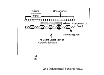
The test platform contains the BUT within a
grounded metallic enclosure 16 (FIG. 3). The purpose of
this enclosure is to provide electromagnetic shielding
for the interior of the test platform.
FIG. 2 illustrates the software procedures
required for the CTS. The sensor control procedure 20
controls the movement and switching of the sensing array.
The spectral analysis procedure 21 receives the measured
results from the spectrum analyzer or the network analy-
zer and calculates, over specific frequency bandwidths,
the integration of the power spectral density (spectral
analyzer mode) or the phase shift (network analyzer mode)
of the acquired signals from the sensors. The calculated
result constitutes pixel values for an image representing
each sensor element at particular locations of the test
plane. Such an image represents the characteristic of
the BUT. The characteristics can then be displayed on
the computer screen with the imaging procedure or passed
on to the fault recognition procedure to determine
whether the BUT is faulty or non-faulty. The fault
recognition procedure is based on a comparison between
the image of the BUT and a known image of a non-faulty
CA 02049616 1999-09-28
- 10 -
board of the same type . Such a comparison results in a
measure of difference between the two boards. If the
difference is larger than a predetermined threshold, the
BUT is diagnosed to be faulty. If the difference is
smaller than the threshold, the BUT is diagnosed to be
non-faulty. Further, regional comparisons can result in
information on the actual location of the faults.
FIG. 3 illustrates the side sectional view of
the test board with a conducting path layout on the board
and an array of sensors above the test board within a
grounded metallic enclosure 16. A sensor array may be
implemented with a stationary sensor array or a small
array of sensors moving across the test plane of the test
board.
Figure 6 illustrates a side sectional view of the
test board with a conducting path layout on the board and
an array of sensors above the test board. In this
arrangement, the energizing signal is applied through a first
conductor 12A of the board for connection to the positive
supply and a second conductor 12B for connection to a
ground return.
CA 02049616 1999-09-28
- 11 -
FIG. 4 illustrates the one dimensional view of
the resultant images obtained according to the above
described procedures. The test board is energized by a
sinusoidal signal (5 volt peak to peak, at a frequency
above 10 MHz). Graph curve (1) is the result of a test
board without the introduced fault (a short). Graph
curve (2) is the result of a test board with the intro-
duced fault (a short). Because of the introduced short
(curve (2)), the adjacent paths are more closely coupled
than without the short (curve (1)), therefore they emit a
higher signal intensity. The two image results can then
be compared to diagnose the fault.
Theoretical background for the solution of loop
antennas and their derivatives results from integrating
the Maxwell-Faraday equation over a loop area Sa and
applying Stokes Theorem thus obtaining
~E'dl'-j~uoffsaH'ds (1)
Consider a printed rectangular spiral antenna-
sensor whose top view is depicted in FIG. 5. The sensor
is exposed to the reactive (or equivalently fringing)
electric and magnetic near-fields surrounding the PCB.
The portion of the near-field coinciding with the fring-
ing field is commonly assumed to exist in the space
confined at the distance 1/K - J~/2n from an equivalent
radiator. The sensor is placed inside a structure which
CA 02049616 1999-09-28
- 12 -
consists of metallic planes of large dimensions. The
distance between the planes is small as compared with the
wavelength of the upper frequency limit of the
applicator. The purpose of this structure is to provide
the eddy current shielding of the interior of the appli-
cator. The Green's function of structure is completely
determined by this geometry of the contactless tester.
The fringing near-field performance of a single
antenna sensor is of interest in response to the standard
fields produced by the chosen radiators.
A printed loop antenna may be modeled as an
uniformly impedance-loaded loop. The boundary conditions
satisfied on the metallic surface S of the sensor
are:
n x (E' - ~- ) -
and
n x (~' - I~ ) =Ys~t ( 3 )
on the dielectric surface Sd. Ys is the surface
admittance of the dielectric layer given by
Ys = j~(E _ Eo)d (4)
Where eo is the substrate permittivity while uo
Equation (1) allows to find a general integral equation
for the zero phase-sequence current by the use of the
generalized Ohm's law '
jWuof oxf G(x,xl)K(xl) ~dSlS =
_Sa _S1 _a _ _
~LZi(1)Ioft)~dl-j~uo~L~LG(X~x1)Io(li)dlldl. (5)
CA 02049616 1999-09-28
- 13 -
The second term on the right hand side
represents interaction due to reradiated field. The
contour integral in (5) is defined for a single loop.
Therefore in order to apply (5) to the printed spiral
antenna, segmentation of a spiral into elementary loops
~is imposed. Then for each loop-segment equation (5) is
valid. The continuity of current I° is
applied at the separation of each constitutive loop.
Equation (5) is not tractable yet for numerical
solution due to the fact both I°(1) and K(X) are unknown
The Lorentz reciprocity theorem applied to the fields
inside the antenna gives second condition which leads to
the integral equation: (6)
E~ySEtdS+f E~I (~)dS=f I (1)'EdV
S° Sm ° ~° °
where E is a function of current K(xl) on the printed
board. Equations (5) and (6) are coupled integral
equations for the unknown currents. In order to solve
the problem, it is natural to use the rectangular
coordinate system because of the geometry in FIG. 5.
Having described the antenna characteristics,
the signal received from the antenna must be processed to
image the BUT's electromagnetic signature.
Denote a signal from each sensor as sij(t)
for i - 1,...N and j - 1,...,M, where t is the time
variable, N and M are the size of the two dimensional
sensor matrix. The pattern of sij(t) is changed by
changes in the signature of the PCB under test.
CA 02049616 1999-09-28
- 14 -
A signal from each sensor can also be
represented in the frequency spectral domain. Denoting
Fourier transform
Fi j (w) =Rij (w) +jXij (w) =Aij (w) e~lj (w) = f ~°sij (t) e-j
wtdt ( 1)
where Ri~(~) and Xi~(m) represent real and imaginary
functions of the Fourier transform of signal si~(t) which
has a frequency spectrum given by
Ai j ( w ) - Ri j w +Xi j w
and
Xij (w)
~ij (w) - arctan
Rij (w)
In the spectral domain, imaging of the PCB
under test (processing in the spatial domain) is obtained
by integrating the spectra in some specific bandwidths.
The result of integration for a single sensor is the pix-
el value (associated with a picture element). The pixel
value is computed for bandwidths where Fi~(~) possesses
high signal-to-noise ratio.
Denoting by K the number of significant
bandwidths, a signature image of a printed circuit board
is defined for the k - th bandwidth in the
following form
CA 02049616 1999-09-28
- 15 -
i=N j=M
Ik (ij ) defy ~fwkLA.~j (~) dw
i=1 j=1
where Ik(ij) represents the power spectrum image in k -
th frequently band ~kL to ~kU~
The phase angle ~(m) may also be used as a
measure of pixel value in an image.