Note: Descriptions are shown in the official language in which they were submitted.
CA 02049900 1998-06-19
TITLE OF THE INVENTION
Video Display Apparatus and
External Storage Unit Used Therein
BACRGROUND OF THE INVENTION
Field of the invention
The present invention relates to a video display
apparatus and an external storage unit used in the
video display apparatus. More specifically, the present
invention relates to a video display apparatus which
displays a plurality of still picture cells (and moving
picture) in an overlaid state onto a monitor screen.
description of the prior art
For example, Japanese patent publication No. 2-
7478 published on February 19, 1990 (corresponding toUS Patent No. 4,824,106) discloses a video display
apparatus to be utilized effectively for a television
game machine or the like. In the prior art, when a
moving picture (object character) and a background or
still picture (still picture character) are displayed
in overlaid state, in order to determine which is to be
displayed at a front side of a monitor screen, priority
data denoted by ~0" or ~1~ is applied, and in a
multiplexer, a moving picture or a still picture having
the priority data being ~1" is selected to be
2~99~
displayed.
When a plurality of still picture cells are used,
the still picture cells can be displayed with the order
inverted utilizing the prior art as above described.
In this method, however, only each still picture cell
as a whole can be inverted. On the other hand, in
order to increase variety of a game or to improve
visual effect, a request occurs to display a plurality
of still picture cells inverted partially, for example,
per each character.
In order to respond to such a reguest, in a case
of utilizing the prior art as above described, still
picture video data may be rewritten during a vertical
tV) blanking period.
However, the still picture video data to be
rewritten are video data of a whole monitor screen of
all of the still picture cells. Particularly, when the
still picture cells are many in number, amount of the
data to be rewritten becomes enormous. Conseguently,
in the prior art, in fact, a plurality of still picture
cells cannot be displayed partially changing the
priority.
SUMMARY OE T~E INVENTION
Therefore, a principal object of the present
invention is to provide a video display apparatus in
which portions of a plurality of still picture cells
can be displayed with the order inverted when the still
picture cells are overlaid.
Another object of the present invention is to
provide an external storage unit which is effectively
used in the above described video display apparatus.
In brief, a video display apparatus in accordance
with the present invention displays a plurality of
still picture cells in an overlaid state, the video
display apparatus comprising still picture video data
generating means for generating video data of a still
picture character to be displayed regarding each of the
plurality of still picture cells, first priority data
applying means for applying first priority data to the
video data of the still picture character from the
still picture video data generating means, selecting
means for determining the priority based on the first
priority data applied to each still picture character
and for selectively outputting the video data of one
still picture character of a still picture having
highest priority among the plurality of still picture
cells, and display means for displaying the still
picture character outputted selectively by the
selecting means.
h?,~9~
An external storage unit in accordance with the
present invention is used in association with a video
display apparatus which displays a plurality of still
picture cells in an overlaid state on a monitor screen
on the basis of video data of still picture characters
generated by a still picture video data generator. The
external storage unit comprises still picture character
code generating means for generating a still picture
character code that designates a still picture
character to be displayed, the still picture character
video data generator generating the video data on the
basis of the still picture character code; and priority
data storing means for storing first priority data that
designates priority of each still picture character.
The video display apparatus includes selecting means
for determining priority of each still picture
character on the basis of the first priority data
applied thereto and for selectively outputting the
video data of one still picture character having the
highest priority of the still picture cell among the
plurality of still picture cells.
The still picture video data generating means
generates, for example, video data (e.g., graphic data
or dot data) of a still picture character of each still
picture cell ~ased on still picture pattern data and
2 ~
character data in accordance with display positions on
a monitor. A microprocessor or CPU applies the first
priority data to the video data of each still picture
character in accordance with a program. The selecting
means includes, for example, a priority encoder and a
decodex, and the priority encoder selects a still
picture character having highest priority and applies
the number of that still picture character to the
decoder. The decoder decodes the number, and outputs a
gate control signal. Consequently, in response to the
gate control signal outputted from the decoder, among
the video data of respective s~ill picture characters
inputted to the selecting means, one still picture
character havin~ the highest priority is outputted from
the qate.
According to the present invention, since the
first priority data is applied per each character of
the still picture cells, and based on this, the
selecting means selectively outputs the video data of
the still picture character of one still picture cell
having the highest priority, the still picture cells
can be easily displayed with the order inverted per
each character.
The objects and other objects, features, aspects
and advantages of the present invention will become
2~'49~
more apparent from the following detailed description
of the embodiments of the present invention when taken
in conjunction with accompanying drawings.
BRIEF DESCRIPTION OF THE DRAWINGS
Figure 1 is a block diagram showing an embodiment
in accordance with the present invention;
Figure 2 is a block diagram showing a timing
signal generator of the embodiment in Figure l;
Figure 3 is a block diagram showing a background
picture data generator of the embodiment in Figure l;
Figure 4 is an illustrative view showing an
example of a data ~ormat of background pattern data;
Figure 5 is a block diagram showing a moving
picture data generator of the embodiment in Figure l;
Figure 6 is an illustrative view showing an
example of a data format of object data (attribute
data);
Figure 7 is a circuit diagram of a transparency
detecting circuit included in a composite circuit of
the embodiment in Figure l;
Figure 8 is a block diagram showing a picture data
control circuit included in the composite circuit of
the embodiment in Figure l;
Figure 9 is a circuit diagram showing a picture
-- 6 --
2 ~
data selecting circuit included in the composite
circuit of the embodiment in Figure l;
Figure 10 is a circuit diagram showing a
modification of the embodiment in Figure 9; and
Figures. llA - llD are illustrative ~iews showing
different display states in the embodiment
respectively, where Figure llA shows mode 0, Figure 11B
shows mode 1, Figure llC shows mode 2, and Figure llD
shows mode 3.
DETAILED DESCRIPTION OF THE P~KRED EMBODIMENTS
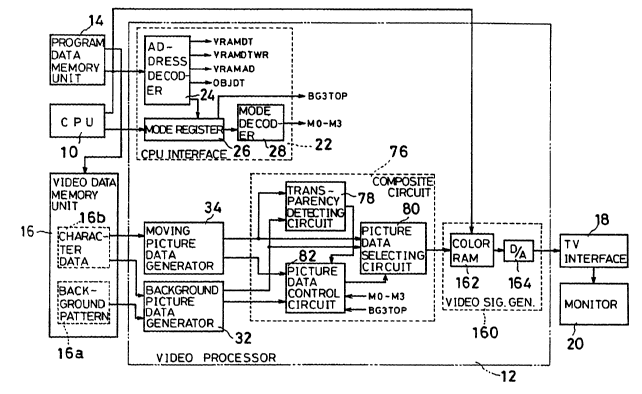
Referring to Figure 1, a CPU 10 controls overall
operation of a picture display apparatus such as a
video processor 12 in accordance with program data from
a program data memory unit 14 included in a memory
cartridqe of detachable type, for example. As the CPU
10, for example, a microprocessor of 16 bits.
The video processor 12 reads graphic data (dot
data) from a video data memory unit 16 in accordance
with command based on the program from the program data
memory unit 14 and thus the microprocessor or CPU 10,
and applies read data to a TV interface 18. The video
data memory unit 16 comprises an SRAM (Static Random
Access Memory) of 64K bytes for example, and includes a
background pattern area 16a and a character data area
2 ~ 0 ~
16b. The background pattern area 16a and the character
data area 16b are in one SRAM as above described,
because the operation speed is rapid and size of the
memory area can be arbitrarily set with respect to the
character (object) and background pattern.
The TV interface 18 converts the graphic data from
the video processor 12 into an RGB signal or TV signal,
and supplies the signal to a monitor 20. Consequently,
on a screen of the monitor 20, with progress of the
program set in advance to the program data memory unit
14, a moving picture (object) of a video game and a
still picture ~background picture) are displayed.
The video processor 12 includes a CPU interface 22
which includes an address decoder 24, a mode register
26 and a mode decoder 28. The address decoder 24
decodes address data outputted from the CPU 10 to an
address bus and applies a latch signal to the mode
register 26, and outputs other necessary timing signals
VRAMDT, VRAMDTWR, VRAMAD and OBJDT. The mode register
2~ 26 latches mode data outputted from the CPU 10 to a
data bus in response to the latch signal from the
address decoder 24, and supplies latched data to the
mode decoder 2a. In addition, such mode data is
programmed in the program data memory unit 14 in
advance, as data of one byte. The mode data is
2 ~ i3
normally programmed at the beginning of the pro~ram,
but a plurality of mode data may be programmed as
necessary. Then, the mode data is read by the CPU 10
to be transferred to the mode register 26. The mode
decoder 2~ decodes the mode data from the mode register
26, and outputs a mode signal MO-M3 representing each
mode described later referring to FIGs. l1A - llD. In
addition, from the mode register 26, a signal BG3Top is
outputted so as to indicate whether or not a specific
background picture cell (in this embodiment, a third
background picture cell BG3 as later described) is to
be displayed at a nearest side on the screen of the
monitor 20. However, as the signal BG3TOP, the most
significant bit of the mode register 26 is outputted as
it is.
The video processor 12 is provided with a timing
signal generator 30 as shown in Figure 2. The timing
signal generator 30 receives a base clock of 21. 47727
MHz for example, and p~ocesses the base clock, for
example, by a counter, a decoder, a logic circuit or
the like thereby prepares necessary timing signals and
supplies the same to respectiYe circuits included in
the video processor 12. For example, i~ the base clock
is subjected to frequency dividing at l/2, a timing
2~ signal /lOM (in the specification, a symbol ~/~ means
2 ~ ~ ~ 9 ~ v
inversion) can be obtained. The signal /lOM is further
subjected to frequency dividing at 1/2, and a resulting
signal corresponds to a display period of one dot
(pixel) on the screen of the monitor 20 (Figure 1). So
by counting this signal, V position data and H position
data respectively indicating a vertical position (V
position) and a horizontal position (~ position) on the
screen of the monitor 20 can be obtained.
A timing signal BGEN is applied to a background
picture data generator 32 (Figure 3) as described later
s~ as to specify a timing when an address is to be
applied to the video data memory unit 16, and a timing
signal O~JEN is applied to a moving picture data
generator 34 as described later so as to specify a
timing when an address is to ~e applied to the video
data memory unit 16. A timing signal ADSW is a signal
to command address changing in the bac~ground picture
data generator 32. A timing signal NDR functions as a
latch signal for a name register 44 (Figure 3) as
described later. A timing signal PDR functions as a
latch signal for a priority data register 46 (Figure 3)
as described later. A timing signal DDR functions as a
latch signal for a dot data register 50 ~Figure 3) as
described later. A timing signal PSLOA~ is a latch
signal which is applied to a P/S converter 52 and a
-- 10 --
~49~
priority data latch 54 '(Figure 3) as described later.
A timing signal PSSHFT is applied to the P/S converter
52 (Figure 3), and functions as a conversion command
signal of the P/S converter 52.
A timing signal DDLD functions as a latch signal
for a dot data register 70 (Figure 5) as described
later. A timing signal PRLD functions as a latch
signal for a priority data register 66 (Figure 5) as
described later. A timing signal PSS~ is applied to a
line buf~er address circuit 64 and a P/S converter 72
(Figure 5) as described later, and the P/S converter
72, receiving the timing signal PSSH, shifts the
character data, and in synchronization with the P/S
converter 72 shifting the data, the line buffer address
circuit 64 increments an address value of a line buffer
74 (Fiqure 5) as described later. A timing signal PSLD
functions as a latch signal for the P/S converter 72.
A timing signal HB is a signal representing a
horizontal blanking period, and is applied to the
moving picture data generator 32 shown in Figure 5 so
that the moving picture data is rewritten during the
horizontal blanking period.
The background picture data generator 32 shown in
Figure 1 will be shown in Figure 3 in detail. In the
background pattern area 16a of the video data memory
2~9~
unit 16, background ~still picture) pattern data shown
in Figure 4 are stored per each background (still
picture) character. More specifically, the background
character data representative of one character includes
name data (character code) of ten(10) bits, color data
of three(3) bits, priority data of one(l) bit and flip
data of two(2) bits. Such background pattern data, in
response to the signal VRAMDTWR from the address
decoder 24 (Figure 1), is written from the program data
memory unit 14 into the video data memory unit 16 by
the CPU 10 through the background picture data
generator 32.
At an initialized state or during the vertical
blanking period, the CPU 10 (Figure 1) outputs a VRAM
address value to the data bus corresponding to a
position of the character on the screen in accordance
with the pro~ram incorporated in the program data
memory unit 14, and outputs a port address to the
address bus corresponding to the address latch 36. The
address decoder 24, receiving the port address, outputs
the latch signal VRAMAD to the address latch 36. The
address latch 36, receiving the signal V~AMAD, latches
~he address ~alue outputted from the CPU 10 at that
tim~. Thereafter, the CPU 10 outputs the name data
indicating a kind of character and the priority data
- ~2 -
~4~
indicating priority of the character to the data bus in
accordance with the program, and outputs a port address
to the address bus corresponding to the video data
memory unit 16. The address decoder 24/ receiving the
port address, supplies the signal VRAMDT to a data gate
38 and an address changing circuit 40, and supplies the
signal VRAMDTWR to the video data memory unit 16. The
data gate 38, receiving the signal VRAMDT, outputs the
data transmitted from the CPU 10 to the data bus at
that time to the video data memory unit l. Receiving
the signal VRAMDT from the address decoder and the
signal BGEN from the timing signal generator 30 (Figure
2~, the address changing circuit 40 applies a content
of the address latch 36 to the video data memory unit
(VRAM) 16. In response to the signal VRAMDTWR, the
video data memory unit 16 writes the name data and the
priority data (Figure 4) from the CPU 10 into the
address outputted from the address changing circuit 40.
Thus, at the initialized state or during the V blanking
period, the background pattern data shown in Figure 4
are written from the CPU 10 into the video data memory
unit 16.
From the video data memory unit 16, the ~ackground
pattern data shown in Figure 4 are read during a
horizontal scanning period. More speci~ically, a VRAM
2 ~ 0 ~
address arithmetic circuit 42 calculates an address
~alue of the background pattern area 16a in the video
data memory unit 16 corresponding to a position of a
scanning line on the screen of the monitor 20 (Figure
1) based on the H position data and the V position data
from the timing signal generator 30, and supplies the
address value to the address changing circuit 40. The
address changing circuit 40 receives the signals ADSW
and BGEN from the timing signal generator 30, and
outputs the address value from the VRDM address
arithmetic circuit 42 to the video data memory unit 16.
When the address value is applied, the background
pattern data shown in Figure 4 are outputted from the
video data memory unit 16. The name data included in
the background pattern data is latched to the name
register 44 in response to the signal NDR from the
timing signal generator 30. The priority data i6
latched to the priority data register 46 in response to
the signal PDR from the timing signal genera~or 30.
A character data address arithmetic circuit 48
calculates an address value of the character data area
16b in the video data memory unit 16 corresponding to a
position of a scanning line on the screen based on the
character code, i.e., the name data latched in the name
z5 register 44 and the V position data applied from the
- 14 -
2~ 9~
timing signal generator 30, and outputs an address
value to the address changing circuit 40. The address
changing circuit 40 applies the address value from the
character data address arithmetic circuit 48 to the
video data memory unit 16 in response to the signals
ADSW and BGEN from the timing signal generator 30.
Accordingly, from the video data memory unit 16,
graphic data (dot data) constituting the character
expressed by the name data is outputted. The dot data
is latched to a dot data register 50 in response to the
signal NDR from the timing signal generator 30. When
data of a plurality of bits per one dot is necessary,
reading of the video data memory unit 16 by the
previous character data address arithmetic circuit 48
is repeated by the number corresponding to the bit
number, and the dot data corresponding to each bit is
latched to the dot data register 50. Furthermore, when
a plurality of background picture cells are displayed,
reading of the above-mentioned name data and the
priority data and reading of the dot data ~re repeated
by the number corresponding to the number of the
~ackground picture ~still picture) cells, and the
priority d~ta and the dot data correspondinq to
respective still picture cells are latched to the
priority data register 46 and the dot data register 50
2~4~
The dot data of the background picture characters
thus latched to the dot data register 50 is latched by
the P/S converter 52 in response to the signal PSLOAD
from the timing signal generator 30. At the same time,
the priority data stored in the priority data register
46 are latched by the priority data latch 54. The P/S
converter 52 and the priority data latch 54 are
prepared respectively by the number corresponding to
the number of the background picture cells, and the dot
data and the priority data of respective background
picture cells are latched simultaneously to the P/S
converter 52 and the priority data latch 54. In
addition, in this embodiment, at most four background
picture cells can be displayed, and it is determined by
the signal M0-M3 from the mode decoder 23 ~Figure 1)
which background picture cell(s) should be used.
The P/S converter 52 converts previously latched
dot data into video data of one dot unit in response to
the signal PSSHFT from the timing signal generator 30.
At the same time, the priority data latch 54 outputs
the priority data to a composite circuit 76 (Figure 1)
described later.
The moving picture data generator 34 shown in
Figure 1 will be shown in Figure 5 in detail. The
moving picture data generator 34 shown in Figure 5
- 16 -
o ~
includes an OAM ~Object Attribute Memory) 56, which has
storage capacity of 34 bits x 128, for example, and can
store object data (attribute data) of objects of total
128 pieces. The object data as shown in Figure 6 is
composed of total 34 bits, and includes object
designating data (name data) of nine(9) bits, V
position data of eight(8) bits, H position data of
nine(9) bits, color data of three(3) bits, priority
data of two(2) bits, flip data of two(2) bits and
object size selecting data of one(l) bit. Such object
data is also written from the program data memory unit
14 into the OAM 56 by the CPU 10 through the moving
picture data generator 34. In addition, an address of
the OAM 56 is designated by an OAM address circuit 58.
More specifically, at an initialized state or
during the V blanking period, the CPU 10 (Figure 1)
outputs an OAM address value to the data bus in
accordance with the program incorporated in the program
data memory unit 14 (Figure 1), and outputs a port
address corresponding to the OAM address circuit 58
into the address bus. The address decoder 24 (Figure
1), receiving the port address, outputs a latch signal
OBJAD to the OAM address circuit 5B. The OAM address
circuit 58 latches the address value of the OAM 56
outputted from the CPU 10 at that time in response to
- ~7 -
2~9~
the signal OBJAD. Thereafter, the CPU 10 outputs the
object data indicating a kind and position of the
moving picture (object) and the priority data
indicating the priority of the object to the data bus,
and outputs a port address corresponding to the OAM 56
into the address bus. Consequently, the signal OBJDT
is outputted from the address decoder 24, and in
response to the signal OBJDT, the object data and the
priority data (attribute data) from the CPU 10 are
written into an address designated by the OAM address
circuit 58 of the OAM 56.
The OAM address circuit 58 receives the signal HB
from the timing signal generator 30 and becomes an in-
range detection mode and, in the in-range detection
mode, the OAM address circuit 58 sequentially applies
addresses from "0~ to "maximum object number minus 1
to the OAM 56. The OAM 56 receives the addresses in
sequence from the OAM address circuit 58, and applies
the V position data and the H position data included in
the object data (Figure 6) to an in-range detection
circuit 60. In the in-range detection circuit 60,
based on the V position data from the timing signal
generator 30, determination is effected as to whether
or not the object is an object to be displayed in a
next scanning line. Regarding only the object to be
- 18 -
2~499~
displayed, the in-range detection signal is applied to
the OAM address circuit 58. The OAM address circuit
58, receiving the in-range detection signal from the
in-range detection circuit 60, writes addresses of the
OAM 56 storing the object data at the in-range state
into an internal memory (not shown).
At the V blanking period, the OAM address circuit
5~ becomes a buffer write mode in response to the
signal HB from the timing signal generator 30. In this
mode, addresses of the object data of the objects
decided being at the in-range state by the in-range
detection circuit 60 are applied in sequence to the OAM
56. On receiving the address from the AM address
circuit 58, the OAM 56 outputs the name data and the
position data among the object data as shown in Figure
6 to a character data address arithmetic circuit 62,
and applies the position data to a line buffer address
circuit 64 and also applies the priority data to a
priority data register 66. The priority data register
66, receiving a signal PRLD from the timing signal
generator 30, latches the priority data. The character
data address arithmetic circuit 62 calculates an
address value of the character data area 16b in the
video data memory unit 16 (Figure l) ~ased on the name
data and the position data of the object as well as the
-- lg --
2~gQ~
V position data from the timing signal generator 30.
The address value is applied to an address changing
circuit 6~. The address changing circuit 68 supplies
the address value outputted from the character data
address arithmetic circuit 62 to the character data
area 16b in response to the signal OBJEN from the
timing signal generator 30.
Consequently, from the character data area 16b,
graphic data (dot data) of the character are outputted
and applied to a dot data register 70. The dot data
register 70 latches the dot data of the object
outputted from the character data area 16b in response
to the signal DDLD from the timing signal generator 30.
A P/S converter 72 loads the dot data of the dot data
register 70 in response to the signal PSLD from the
timing signal generator 30.
The line buffer address circuit 64 is set to a
line buffer write mode in response to the signal HB
from the timing signal generator 30. In this mode, the
line buffer address circuit 64 calculates an address
value of the line buffer 74 based on the position data
includPd in the object data inputted from the OA~ 56~
The line buffer 74, receiving the address from the line
buf~er address circuit 64, stores the dot data from the
P/S converter 72 and the priority data from the
- 20 -
h
priority data register 66.
After the line buffer 74 stores the dot data of
one dot, the P/S converter 72 shifts the dot data in
response to the signal PSSH from the timing signal
generator 30, and applies the picture data in one dot
unit to the line buffer 74. Also the line buffer
address circuit 64 increments the address value in
synchronization with data shifting in the P/S converter
72.
At the horizontal scanning period, the line buffer
address circuit 64 is set to a line buffer read mode in
response to the signal HB from the timing signal
generator 30. In this mode, the line buffer address
circuit 64 sequentially supplies the address values
from "0" to ~maximum dot number in horizontal direction
minus 1" to the line buffer 74. Accordingly, from the
line buffer 74, the object dot data and the priority
data are outputted in sequence to be applied to a
subsequent composite circuit 76 ~Figure 1).
~ hus, the dot data and the priority data per each
character of the background picture are outputted from
the background picture data generator 32, and the dot
data and the priority data of the object character are
outputted from the moving picture data generator 34.
2~
These data are applied to the composite circuit 76
2 ~ L~
shown in Figure 1. That is, respective dot data are
applied to a transparency detecting circuit 78 and a
picture data selecting circuit 80, and the priority
data are applied to a picture data control circuit 82.
The signals M0-M3 and BG3TOP from the CPU interface are
supplied to the picture data control circuit 82.
The transparency detecting circuit 78 includes
five OR gates 84, 86, 88, 90 and 92 as shown in Figure
7. Inverted dot data of a first background picture
lQ cell BGl from the P/S converter 52 (Figure 3) of the
background picture data generator 32 are inputted to
the OR gate 84, inverted dot data of a second
background picture cell BG2 are inputted to the OR gate
86, inverted dot data of the third background picture
cell BG3 are inputted to the OR gate 88, and inverted
dot data of a fourth background picture cell BG4 are
inputted to the OR gate 90. The dot data of these
background picture cells BGl-BG4 are 2-8 bits. On the
other hand, inverted dot data of the object being
fourl4) bits are applied to the OR gate 92. From the
OR gates 84, 86, 88, 90 and 92, when any of each input
is "~", decision is effected that each character is
transparent, and signals /BGlCLR, /BG2CLR, /BG3CLR,
/~G4CLR and /OBJCLR to make the priority data
ineffecti~e are outputted to be supplied to the picture
2 ~
data control circuit 82 (Figure 1 and Figure 8).
The signal /BGlCLR from the transparency detecting
circuit 78 is supplied to respective one inputs of NAND
gates 94 and 96 of the picture data control circuit 82
shown in Figure 8. Priority data BGlPRI and its
inversion of the first background picture cell are
applied to respective other inputs of the NAND gates ~4
and 96. Also the signal /BG2CLR from the transparency
detecting circuit 78 is inputted to one inputs of NAND
gates 98 and 100, and the priority data BG2PRI and its
inversion of the second background picture cell are
applied to other inputs of the NAND gates 98 and 100.
~he signal /BG3CLR from the transparency detecting
circuit 78 is supplied to one inputs of NAND gates 102
and 104, and the priority data ~G3PRI and its inversion
of the third background picture cell are applied to
other inputs of the NAND gates 102 and 104. The signal
/BG4CLR is supplied to one inputs of NAND gates 106 and
108, and the priority data BG4PRI and its inversion of
the fourth background picture cell are applied to other
inputs of the NAND gates 106 and 108. Furthermore, the
signal /OBJCLR from the transparency detecting circuit
is supplied to respective one inputs of four NAND gates
110, 112, 114 and 116. Priority data ~BJPRI (two bits)
included in the object data are applied to a decoder
- 2~ -
2~9~0
118. The decoder 118 decodes the priority data OBJPRI
of two(2) bits and outputs signals indicating the four
states, and the signals are supplied to other inputs of
the NAND gates 110, 112, 114 and 116, respectively.
Inverted signals of the signals M0 and Ml from the
mode decoder 28 (Figure 1) are supplied to two inputs
of a OR gate 120, and the signal Ml is supplied to one
input of an OR gate 122. Inversion of the signal
BG3TOP is supplied to one input of the OR gate 122, and
inversion of output of the NAND gate 102 is further
supplied to one input ~f the OR gate 122. Respective
inverted outputs of NAND gates 112, 114 and 116 are
supplied to respective one inputs of OR gates 124, 126
and 128, and inverted output of the OR gate 120 is
supplied to respective other inputs of these OR gates
124 - 128.
A priority encoder 130 selects one having the
highest priority among pictures where priority data are
effective, and applies its number to a subse~uent
decoder 132. The priority encoder 130 has 16 inputs P0
- P15. The input P0 is grounded. The inputs Pl, P2,
P3, P4, P5, P6, P7, P8, P9, P10, Pll, P12, P13, P14 and
PlS are supplied with outputs of the ~A~D gates 10~,
104, 116, 106, 102, 114 and 100, the O~ gate 128, the
NAND gates 96 and 112, the OR gate 126, the NAND gate
- 24 -
2~9~0~
98, the OR gates 124 and the NAND gates 94 and 110,
respectively.
Thus, respective priority data are decoded by
respective NAND gates and become a plurality of picture
output signals, but only one picture output signal
shown by the priority data is effective. Since the
priority data exist per each screen (still picture cell
and object), effective picture output signals exist by
the screen number. On the other hand, all the picture
output signals of the screen having the transparent
picture data are made ineffective by the clear signals
from the transparent detecting circuit 78, and only the
picture output signals of the screen having the dot
data being not transparent are made effective.
Respective picture output signals are inputted to NAND
gates together with the mode signals, and are further
made effective or ineffective by values of the mode
signals M0 and Ml to be inputted to the priority
encoder 130. Consequently, signals being made
effective by the priority encoder 130 are (a) the
priority data of the background picture and the moving
picture in the number set by the mode at that time, (b)
the picture output signals generated respectively by
selecting only one screen position among a plurality of
picture positions peculiar to each screen (cell) by
2 ~
value of the priority data, (c) the picture output
signals of the screen where the picture data are not
transparent, and (d) the picture output signals made
effective by setting the basic priority by the mode
data. Thus, the priority encoder 130 selects one
having the highest priority among the effective picture
output signals.
Signals outputted from the priority encoder 130
are supplied to the decoder 132 which decodes the
number from the priority encoder, and only one picture
output signal shown by the number is made effective
among all picture output signals. Only one picture
output signals being made effective is latched to a
data latch 144 by AND gates 134 - 140 as a dot data
output selection signal that shows which dot data
should be outputted. Consequently, from the data latch
144, dot data output selection signals /OBJSEL,
/BGlSEL, /BG2SEL, /BG3SEL and /BG4SEL are outputted.
Since the priority data input terminal P0 of the
priority encoder 130 is always supplied with an output
signal of the background color data, when all the
picture output signals are made ineffective, the
background color data selection siqnal /~ACK is
outputted. The selection signal is supplied to the
picture data selecting circuit ~0 (Figure 1 and ~igure
- 26 -
2 ~
9) ~
The picture data selecting circuit 80 with its
detail shown in Figure 9 includes six tri-state buffers
146 - 156 and further has a background color data
generator 158. BGl dot data from the background
picture data generator 32 is inputted to the tri-state
buffer 146, and the signal /BGlSEL from the picture
data control circuit 82 is applied as its control
input. Also the tri-state buffers 148, 150, 152 and
154 are respectively supplied with BG2 dot data and the
signal /BG2SEL, BG3 dot data and the signal /BG3SEL,
BG4 dot data and the signal /BG4SEL as well as OBJ dot
data and the signal /OBJSEL. The tri-state buffer 156
is supplied with an output from the background color
data generator 158, and its control input is supplied
with the background color selection signal /BACK.
Consequently, the picture data selecting circuit 80
selects the dot data corresponding to only one picture
output signal made effective by the picture data
control signal 82 or the background color data, and
supplies the selected data as color data to a
subsequent ~ideo signal generator 160.
In addition, the picture data selecting circuit 8
may be modified as shown in Figure 10. In Figure 10,
an output of each of the tri-state buffers 146 - 154
2~9~
and the background color selection signal /BACK are
supplied to an AND gate of the background data
generator 158. Consequently, only when the background
color selection signal /8ACK is at a low level, dot
data outputted from any of the tri-state buffers 146 -
154 are selected.
Thus, the color data outputted from the picture
data selecting circuit 80 are supplied to the video
signal generator 160 shown in Figure 1. The video
signal generator 160 includes a color RAM 162 and a D/A
converter 164. The color RAM 162 is a color table to
derive color data using the dot data as address, and
the color table is first written by the CPU 10.
Consequently, a color signal selected in accordance
with the color data from the picture data selecting
circuit 80 is supplied to the D/A con~erter, and the
color data is converted into a voltage level to be
supplied to the TV interface 18.
Thus, the priority is applied per each character,
and based on this, the priority is determined so that
the picture data having the highest priority per each
character unit is displayed on the monitor 20 ~Figure
1). This will be described in detail referring to
FI~s. llA - llD.
Figure llA shows a case of mode 0 specified by the
- 28 -
2~g~
signal M0 from the mode decoder 28 (Figure 1). In this
case, the first, second, third and fourth background
picture cells BGl, BG2, BG3 and BG4 are all used.
When the priority data PRI of the background
pattern data (Figure 3) of each background picture cell
are all set to "0" in the characters of the background
picture cells expressed by the name codes, as shown by
a dotted line in Figure llA, the background picture
cells BGl, BG2, BG3 and BG4 are displayed from the
front side of the monitor screen towards the back side
in this order, and the background color is displayed at
the most back side of the monitor screen by the
background color data prepared in Figure 9 or Figure
10 .
When the priority data of the characters of the
second background picture cell BG2 is set to "1" and
the priority data of other background picture cells BGl
~G3 and BG4 are set to "0", the characters of the
second background picture cell BG2 is displayed at the
front side of the monitor screen with respect to the
first background picture cell BGl as shown by a solid
line in Figure llA That is, in this case, the
character of the second background picture cell B&2 is
displayed with priority.
Also when the priority data of the characters of
- 29 -
the fourth background picture cell BG4 are only set to
~1", the character of the fourth background picture
cell BG4 are displayed at the front side with respect
to the characters of the third background picture cell
BG3 as shown by a solid line in Figure llA.
In the mode 0, the signal /BG3TOP to display the
third background picture cell BG3 at the nearest side
of the monitor screen is ineffective.
Regarding the object, when the priority data PRI
included in the object data (attribute data) shown in
Figure 6 is set to ~11", irrespective of the priority
data of the background pattern data, the object
character is displayed at the front side of the monitor
screen with respect to all background picture cells.
When the priority data of the object data is set to
~10~, the object is displayed at the nearest side of
the monitor screen if the priority data of any of the
first background picture cell BGl and the second
background picture cell BG2 are set to "0~. When the
priority data included in the object data is set to
ffOl~, the object is displayed at the rear side with
respect to the second background picture cell BG2
having the priority data being set to "on. When the
priority data included in the object data is set to
~00", the obiect is displayed at the front side with
- 30 -
2~499~
respect to the characters of the third background
picture cell BG3 if the priority data of the third
background picture cell BG3 are set to "0~.
The mode 1 shown in Figure llB is specified by the
signal Ml from the mode decoder 2B (Figure 1). In this
case, the fourth background picture cell BG4 is not
used although it is used in Figure llA, and the signal
BG3TOP to display the third bac~ground picture cell at
the nearest side of the monit~r screen is made
effective. Consequently, when the signal BG3TOP is set
from the CPU 10 to the mode register 26 (Figure 1), the
third background picture cell BG3 is displayed at the
nearest side of the monitor screen as shown by a solid
line in Figure llB. However, when the signal BG3TOP is
set to ~0~, the character of the third background
picture cell BG3 is displayed at the most back side of
the monitor screen, irrespective of the priority data
PRI.
The third background cell BG3 is set, for example,
as the screen with little color number such as numeric
characters. When the signal BG3TOP to display the
third background picture cell BG3 at the nearest side
is set, the third background picture cell as a whole is
displayed at the nearest side.
When the priority data PRI (Figure 4) of the
- 31 -
2 ~ 4 9 9 0 ~
background pattern data of any of the first, second and
third background picture cells is set to ~0" and the
signal BG3TOP is set to "0", as shown in Figure llB,
the first, second and third background picture cells
BGl, BG2 and BG3 are displayed from the front side of
the monitor screen in this order. If the priority data
of the second background picture cell is set to "1", in
similar manner to Figure llA, the character of the
second background picture cell BG2 is displayed at the
front side with respect to the first background picture
cell BGl. The object is as described in Figure llA.
Referring to Figure llC, the mode 2 is specified
by the signal M2 from the mode register 28 (Figure 1),
and only the first and second background plcture cells
BGl and BG2 are used. Consequently, in the mode 2, the
third and fourth background picture cells BG3 and BG4
as well as the signal BG3TOP are ineffective. When the
priority data of any of the first and second background
picture cells BGl and BG2 is set to ~0", as shown in
Figure llC, the characters of the the first background
picture cell BGl and the second background picture cell
B~2 are displayed from the front side of the monitor
screen in this order. When the priority data of the
second background picture cell BG2 is set to ~1", the
character of the second background picture cell BG2 is
- 32 -
2 ~
displayed at the front side with respect to the first
background picture cell BGl.
Regarding the object, when the priority data
included in the object data is "11", the object is
displayed at the front side with respect to the
character of the first background picture cell BGl
having the priority data being ~1~. When the priority
data of the object data is set to "10", the object is
displayed at the back side with respect to the
character of the first background picture cell BGl
having the priority data being ~1~ and at the front
side with respect to the character of the second
background picture cell BG2 having the priority data
being set to ~ln. When the priority data of the object
data is set to "01", the object is set between the
second bac~ground cell BG2 having the priority data
being ~1~ and the first background cell BGl having the
priority data being "on. When the priority data of the
object data is set to "00", the object is displayed
between the first and second background picture cells
BGl and ~G2, both having the priority data being set to
non .
The mode 3 shown in Figure llD is specified by the
signal M3 from the mode register 28 ~Figure 1), and
only the first background picture cell BGl is used in
the mode 3. Consequently, the second - fourth
background picture cells BG2 - BG4 as well as the
signal BG3TOP are ineffective. In the mode 3, when the
priority data of the object data is set to ~ , the
S object is displayed at the front side with respect to
the first background picture cell BGl having the
priority data being set to ~1". However, when the
priority data of the object data is set to "10" or
"01", the object is displayed at the back side with
respect to the characters of the first background
picture cell ~Gl having the priority data being set to
~1~. However, when the priority data of the first
background picture cell BGl is set to "o", the object
having the priority data being set to "10" or "01" is
displayed at the front side. The object having the
priority data being set to "00" is displayed at the
most back side of the monitor screen.
In addition, a memory cartridge incorporating a
semiconductor memory is used as an external storage
unit in the above described embodiments; however, it is
possible to use an external storage unit s~ch as a CD-
ROM in the present invention. In a case of use of the
memory cartridge, the program data including the
character data, color data, priority data~ mode data
and etc. that are described previously is stored in the
- 34 -
2 ~ 0 ~
semiconductor memory, and the CPU 10 generates control
data for the moving picture characters and the still
(background) picture characters on the basis of the
program data read from the semi~onductor memory and
outputs the same to the video processor 12.
In contrast, in a case of use of the CD-ROM, the
above described program data is optically recorded as
digital data in the C~-ROM (not shown). In addition,
an optical reader for optically reading recorded date
on the CD-ROM is connected to a suitable connector such
as a expansion connector. When the CD-ROM is used as
the external storage unit, a memory cartridge is also
used. In this case, the memory cartridge is comprised
with a ROM (not shown) that stores a starting proqram
for controlling an operation of the optical reader, a
buffer RAM (not shown) for temporarily storing the
program data read from the C~-ROM, and etc. Then,
prior to a start of a display operation, the CPU 10
applies control data to the optical reader on the basis
of the starting program of the ROM to cause the optical
reader read the recorded data ~f the CD-~OM. R portion
of the character data read from the CD-ROM is
transferred to the character RAM and the program data
is transferred to the buffer RAM included in the memory
cartridge. The CPU 10 controls the video processor 12
- 35 -
2 ~ LJL ~
on the basis of the program data stored in the buffer
RAM. That is, after the data read from the CD-ROM by
the optical reader has been transferred to the
respective memories, the CPU 10 and the video processor
12 execute the display operation by accessing the
respective memories as done in the previous
embodiments.
Although the present invention has been described
and illustrated in detail, it is clearly understood
that the same is by way of illustration and example
only and is not to be taken by way of limitation, the
spirit and scope of the present invention being limited
only by the terms of the appended claims.