Note: Descriptions are shown in the official language in which they were submitted.
~04g~t ~
..~
APPARATUS FOR TESTING ATM CHANNELS
Backqround of the Invention
Field of the Invention
Thls invention pertains to a digital switching
system and more particularly to an apparatus
for testing ATM (Asynchronous Transfer Mode) channels,
according to a multi-stage self-routing method, to
integrally switch information having different traffic
characteristics, such as moving images, numerical data
and voices, by using an ATM transmission system like a
broadband ISDN.
Description of the Related Art
With the widespread use of data communication,
public switched networks are now required to execute
high-quality data communication, as well as the
traditional voice communication.
A Broadband Integrated Services Digital Network
(B-ISDN) has begun to be utilized as a communication
network not only for low-speed data, such as voice
data, but also for high-speed data between 150 Mbps
and 600 Mbps, such as moving images, and various
interfaces have begun to be standardized. CCITT
(International Telegraph and Telephone Consultative
Committee) is currently working on its advisory report
on the ATM transmission system, which is an essential
technology for realizing a B-ISDN, to be submitted in
1992.
An ATM communication network transmits and
exchanges information of different bands divided and
housed in fixed-length data units called cells, to
which headers are added. A header contains a
virtual channel identifier (VCI) for identifying the
receiving side subscriber. Thus, an ATM switching
system uses the headers to enable hardware to transfer
and switch cells to the receiving side subscriber at a
high speed.
Since an ATM system requires cells to carry only
necessary information, it can more efficiently
transmit bust signals than a conventional STM
(Synchronous Transfer Mode) system. Also, unlike a
conventional packet switching system that has a
processor switch cells equivalent to packets through
software processing, since an ATM system has hardware
provided in a channel switch cells, it does not
require complex protocols in switching cells, which
realizes high speed communication at up to several
hundred mega bits a second.
2 ~
This makes it possible to flexibly provide
services requiring different transmission speeds, and
to efficiently utilize transmission paths.
In this operation, according to the VCI attached
to a cell, a switching system processor designates to
which buffer in a switch of the ATM switching system
the cell is to be written. The cells flow
autonomously in the network according to this
designation. Hence, this switching operating is
called a self-routing (SR). The receiving side
subscriber extracts necessary cells flowing over ATM
highways based on the VCIs attached to cells, and
restores user information by eliminatiny headers from
the cells.
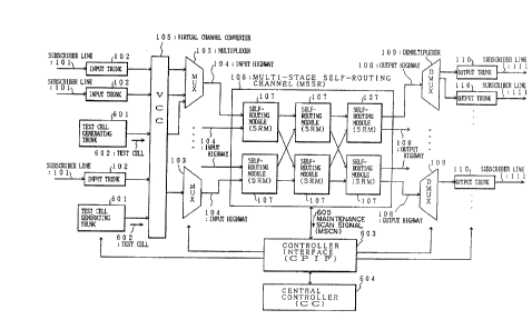
Figure 1 is a schematic view of a generic ATM
switching system.
In Figure 1, trunks 102 accommodate respective
subscriber lines 101 on the input side. A virtual
channel controller (VCC) 105 receives outputs from the
trunks 102.
Based on the call control information inputted
from a processor (not shown) of the switching system,
the VCC 105 exchanges the VCIs, which specify the
cells' destinations, attached to the headers of the
received cells from the respective input highways 104,
2 ~
with new VCIs specifying the next output node (ATM
switching system). At the same time, the VCC 105
adds to the head ends of the cells information
specifying the path over which the cells are to be
switched to be outputted to destined output highways
108 in a data format called tags.
A plurality of multiplexers (MUXs) 103 partially
multiplex respective outputs from the VCC 105.
Respective input highways 104 receive outputs from the
corresponding multiplexers 103.
A multi-stage self-routing channel (MSSR) 106,
which is a virtual channel, receives respective
outputs from the MUXs 105. The MSSR 106 comprises a
plurality of self-routing modules (SRMs) 107. The
MSSR 106 has a plurality (ordinarily two (2) rows and
three (3) stages) of SRMs 107. The configuration of
the SRMs 107 are further elaborated later.
The MSSR cells to output highways
108, which are connected to respective demultiplexers
(DMUXs) 109, which demultiplex the cells and output
the demultiplexed cells to subscriber lines 111 on the
output side through output trunks 110 corresponding to
the respective DMUXs 109.
Figure 1 shows a configuration where cells flow
in a single direction over the channels. It goes
2 ~
-- 5
without saying that channels for cells flowing in the
opposite directions can be configured similarly.
Figure 2 shows an exemplary configuration of one
of the SRMs 107 shown in Figure 1.
In the example shown in Figure 2, an SRM 107 has
two (2) input lines and two (2) output lines, and
switches 201 provided at the four (4) crossing points
of the input lines and output lines. That is, the
four (4) switches of an SRM 107 correspond with two
(2) input lines and two (2) output lines. Although
an actual channel comprises more input lines and more
output lines in reality, since their basic connections
are entirely similar to those in the example shown in
Figure 2, the SRMs 107 are explained by referring to
the 2X2 exemplary configuration having two (2) input
lines and two (2) output lines.
The switches 201 judge from the tag data attached
to the head ends of cells inputted from input lines
whether or not to switch the cells for acceptance.
If the switches 201 judge to switch the cells, the
switches 201 multiplex the cells on free time slots on
output lines. Respective switches 201 independently
perform the judging and switching operations through
hardware processing.
As is evident from the above explanation, a fault
3~
in one of the switches 201 in any of the SRMs 107
shown in Figure 1 causes a severe fault, such as a
degradation in communication quality and a stoppage of
communication through discarding ATM cells and
incorrectly switching ATM cells. Therefore, it is
crucial to conduct a test for verifying the normality
of the switches.
However, there is no known conventional system
for efficiently testing the switches of an ATM
switching system. Especially in the configuration,
shown in Figure 1, of the MSSR 106 having the SRMs 107
connected in a plurality of stages, the more there are
possible paths from an input line to an output line,
the more there are the SRMs 107 in the MSSR 106.
This causes an inevitable problem of how to
efficiently test all such possible paths in realizing
an ATM switching system.
I. a
Summary of the Invention
This invention is conceived based on the above
background, and aims at efficiently testing all paths
in an ATM channel configured by respective switches.
A first form of this invention utilizes the
following elements.
A test cell generating trunk is provided on the
input side of an asynchronous transfer mode channel
e.g. comprising a multi-stage self-routing channel
having plural stages of self-routing modules. It
generates a test cell having a tag at the head end and
inputs the test cell to the asynchronous transfer mode
channel. The tag stores test cell data for test
cell identification and for specifying the passage of
a predetermined path in the asynchronous transfer mode
channel.
Test cell detectors are provided respectively in
the switches forming the asynchronous transfer mode
channel. Each of them detects, as a maintenance
scan signal, whether or not the test cell is switched.
A controller tests the switches on a path
corresponding to the test cell data stored in a test
cell by judging, in synchronization with test cell
generation, whether or not the test cell detectors of the
switches of the path detect maintenance scan signals.
In accordance with the present lnventlon, there is
provided an asynchronous transfer mode channel testlng
apparatus for testlng an asynchronous transfer mode channel,
the asynchronous transfer mode channel having swltches therein
to direct traffic, comprlsing:
test cell generatlng trunk means, provlded on an
lnput side of said asynchronous transfer mode channel, for
generating a test cell having a tag attached a header thereof,
the tag including test cell information which speclfles a
partlcular path in the asynchronous transfer mode channel to
be tested, said test cell generating trunk means supplying the
test cell to the asynchronous transfer mode channel to be
tested;
test cell detecting means, provlded ln each of a
plurality of the swltches of the asynchronous transfer mode
channel, for detectlng whether a switch along the partlcular
path specifled by the test cell has swltched the test cell and
provldlng a malntenance scan slgnal lndicative of a result of
the detecting; and
controlling means for testing the switch along the
particular path speclfled by the test cell by judglng whether
sald test cell detectlng means provides the maintenance scan
slgnal.
The above described first form of this invention
enables swltches to be tested under actual operation wlthout
interrupting channel processing, e.g. by inputting a test cell
- 8 -
,
28151-45
~ ~ 4 ~
.,._
to an asynchronous transfer mode channel at a free cell timing
on an lnput highway.
Because the test cell generating trunk generates
test cells havlng tags at the head ends storing test cell data
collectlvely specifying the passages of all switches in the
asynchronous transfer mode channel relevant to the input
highway connected to the test cell generating trunk, and
because the controller collect all maintenance signals from
the test cell detectors in the respective swltches, lt becomes
possible to perform efficient tests.
The above described first form of this invention
enables an asynchronous transfer mode channel to be
efficiently tested, even when the channel has a complex
configuratlon, such that the channel is a multi-stage self
routing module with self-routlng modules each havlng switches
connected in plural stages.
The controller enables a simple control to test
- 8a -
28151-45
J ~. ~
"~
switches with ease, e.g. by judging whether or not the
test cell detector of a switch on a path corresponding
to the test cell data stored in a test cell detects a
maintenance scan signal in a predetermined time period
after the test cell is generated.
A second form of this invention utilizes the
following elements.
Test cell generators are provided for respective
input highways. A test cell generator sequentially
generates a plurality of test cells. The test cells
are switched at crossing points in all self-routing
modules, where cells inputted from the input highway
corresponding to the test cell generator pass through.
The test cells have test cell identification data for
identifying the test cells and the input highway
identification data.
Test cell monitors are provided for respective
output highways. A test cell monitor monitors
whether or not a predetermined number of test cells
corresponding to the number of paths on all self-
routing modules, through which cells inputted from
each of the input highways pass to be outputted to
each of the output highways, by extracting by test
cell identification data test cells from cells
9~1~
-- ~o --
outputted from self-routing modules to respective
output highways and by extracting input highway
identification data from the extracted test cells.
The above described second form of this invention
enables an asynchronous transfer mode channel to be
tested with ease by simply counting the numbers of
test cells from respective input highways, without
having to collect information from respective crossing
points in self-routing modules regarding whether or
not the crossing points switch test cells.
In this case, the test cell generators and the
test cell monitors respectively need to be provided
only for the numbers of the input highways and output
highways, and their configurations are simple.
Therefore, a configuration far simpler than a
conventional configuration, where all crossing points
in the self-routing modules have test cell detectors,
realizes testing a channel.
A third form of this invention utilizes the
following elements.
A test cell generating trunk is provided on the
input side of an asynchronous transfer mode channel.
It generates a test cell whose header part has a test
cell indication bit for test cell identification and
supplies it to the asynchronous transfer mode channel.
Turnaround parts are provided in the ordinary
trunks respectively connecting external transmission
paths and asynchronous transfer mode channel. Each
turnaround part extracts by test cell indication bits
test cells from cells transmitted through an
asynchronous transfer mode channel, and turns the
extracted test cells around to the test paths in the
asynchronous transfer mode channel.
Here, the test cell generating trunk stores in
the information parts of test cells path selection
data specifying the test paths in the asynchronous
transfer mode channel. In addition to the above
configuration, a tag operator can be provided between
the turnaround parts and the asynchronous transfer
mode channel. The tag operator replaces the tags
attached to the head ends of the test cells turned
around by the turnaround part in an ordinary trunk
with others based on the route selection data stored
in the information parts of the test cells, and
then supplies the reconfigured test cells to the
asynchronous transfer rnode channel.
Further, the test cell generating trunk stores in
the information parts of test cells path selection
data specifying the test paths, terminated at the test
~4~
,.~
cell generating trunk, in the asynchronous transfer
mode channel. In addition to the above
configuration, a controller for testing an
asynchronous transfer mode channel can be provided at
5 the test cell generating trunk. It judges whether
or not test cells generated by the test cell
generating trunk return to the test cell generating
trunk. It compares the contents of the test cells
generated from thé test cell generating trunk with the
10 contents of the test cells returned to the test cell
generating trunk.
The above described third form of this invention
enables an asynchronous transf er mode channel to be
tested with lesser hardware comprising only a test
15 cell generating trunk and turnaround parts
respectively provided in ordinary trunks, because test
cells generated from a test cell generating trunk are
sequentially turned around in the turnaround parts in
ordinary trunks to be returned finally to the test
20 cell generating trunk.
Brief Description of the Drawings
Those in the same field can easily understand
additional purposes and features of this invention
from the descriptions of the principles and the
preferred embodiments of this invention together with
the attached drawings. In the drawings;
Figure 1 is a schematic view of a generic ATM
switching system;
Figure 2 shows an exemplary configuration of one
of the SRMs shown in Figure 1;
Figure 3 is a schematic view for explaining a
first form of this invention;
Figure 4A is a schematic view for explaining a
second form of this invention;
Figure 4B shows the data structure of a test cell
in the second form of this invention;
Figure 5 is a schematic view for explaining a
third form of this invention;
Figure 6 is a block diagram of a first preferred
embodiment of this invention;
Figure 7 shows the configuration of a switch in
an SRM in the first preferred embodiment;
Figure 8A shows the data configuration of an ATM
cell in the first preferred embodiment;
o
Flgure 8B shows the conflguratlon of the tag part of an
ATM cell shown ln Flgure 8A;
Flgure g ls a block dlagram of a second preferred
embodlment of thls invention;
Flgure 10 shows the conflguratlon of the MSSR ln the
second preferred embodlment;
Flgure 11 shows the conflguratlon of an SRM ln the second
preferred embodlment;
Flgure 12 shows the conflguratlon of the VCC ln the
second preferred embodlment;
Flgure 13 shows the conflguratlon of a crosslng polnt ln
the second preferred embodlment;
Flgure 14 shows the conflguratlon of an ATM cell in the
second preferred embodlment;
Flgure 15 shows the tag datum comblnatlons ln tag parts
attached to test cells ln the second preferred embodlment;
Figure 16 shows the conflguratlon of the TCC (test cell
monitor) ln the second preferred embodlment;
Flgure 17 ls a block dlagram of a thlrd preferred
embodlment of thls lnventlon;
Flgure 18 shows the configuration of the test cell
generatlng trunk ln the thlrd preferred embodlment;
Flgure 19 shows the conflguratlon of the
28151-45
- 15 -
turnaround part of a tested trunk in the third
preferred embodiment;
Figure 20 shows the data format of a transmission
path in the third preferred embodiment;
Figure 21 illustrates the cell format conversion
in the third preferred embodiment; and
Figure 22 shows the configuration of the tag
operator in an multiplexer in the third preferred
embodiment.
1 0
Description of the Preferred Embodiments
Explanation of the Principles
Before describing the preferred embodiments of
5 this invention, its principles are explained.
Figure 3 is a schematic view for explaining a
first form of this invention.
A test cell generating trunk 302 is provided on
the input side of an asynchronous transfer mode
channel 301 . The test cell generating trunk 302
generates a test cell 303 having a tag 304 at the head
end and inputs the test cell 303 to the asynchronous
transfer mode channel 301. The tag 304 stores test
cell data 305 for test cell identification and for
specifying the passage of a predetermined path in the
asynchronous transfer mode channel 301.
Here, the asynchronous transfer mode channel 301
is a multi-stage self-routing channel e.g. having
plural stages of self-routing modules. As shown in
20 Figure 3, it switches a cell inputted from an input
highway 310 and output it to an output highway 311.
Input highways 310 connected to the input side of
the asynchronous transfer mode channel 301 have the
respective test cell generating trunks 302, which
25 multiplex the test cells 303 on the corresponding
input highways 310 at a free cell timing of the input
highways 310.
As already stated, the test cell generating trunk
302 generates a test cell 303 having a tag 304 at the
head end and inputs the test cell 303 to the
asynchronous transfer mode channel 301. The tag 304
stores test cell data 305 for test cell identification
and for specifying the passage of all switches 306,
relevant to the input highways 310 corresponding to
the test cell generating trunk 302, in the
asynchronous transfer mode channel 301.
Test cell detectors 307 are provided respectively
in the switches 306 forming the asynchronous transfer
mode channel 301. Each of them detects, as a
maintenance scan signal 308, whether or not the test
cell 303 is switched.
A controller 309 tests the switches 306 on a path
corresponding to the test cell data stored in a test
cell 303 by judging, in synchronization with test cell
generation, whether or not the test cell detectors 307
of the switches 306 of the path detect maintenance
scan signals 308.
The controller 309 tests switches 306 on the path
corresponding to the test cell data 305 stored in the
test cell 303, e.g. by judging whether or not the test
~J ~
- 18 -
cell detector 307 of a switch 306 on a path detects a
maintenance scan signal in a predetermined time period
after the test cell 303 is generated. The
controller 309 is e.g. the central controller of the
ATM switching system.
The above described configuration shown in Figure
3, where the input highways 310 connected to the input
side of the asynchronous transfer mode channel 301
respectively have the test cell generating trunks 302,
enables switches 306 to be tested under actual
operation without interrupting channel processing,
e.g. by multiplexing a test cell 303 on the input
highways 310 at a free cell timing.
The test cell generating trunk 302 generates test
cells 303 having tags 304 at the head ends storing
test cell data 305 collectively specifying the
passages of all switches 306 in the asynchronous
transfer mode channel 301 r~elevant to the input
highway 310 connected to the test cell generating
trunk 302. The controller 309 collect all
maintenance signals 308 from the test cell detectors
307 in the respective switches 306. These
operations enable tests to be performed efficiently.
The above described configuration shown in Figure
3 enables an asynchronous transfer mode channel to be
- 19 -
efficiently tested, even when the asynchronous
transfer mode channel 301 has a complex configuration,
such that the asynchronous transfer mode channel 301
is a multi-stage self-routing module with self-routing
modules each having switches 306 connected in plural
stages.
The controller 309 enables a simple control to
test switches 306 with ease, e.g. by judging whether
or not the test cell detector 307 of a switch 306 on a
path corresponding to the test cell data 305 stored in
a test cell 303 detects a maintenance scan signal 308
in a predetermined time period after the test cell 303
is generated.
Figure 4A is a schematic view for explaining a
second form of this invention, and Figure 4B shows the
data structure of a test cell in the second form of
this invention.
The second form of this invention is premised on
an ATM channel formed by a multi-stage self-routing
channel, comprising self-routing modules 401 connected
in plural stages, for switching for connection
respective cells inputted from a plurality (any of #0
through #n-1, where n is a integer) of input highways
402 to a plurality (any of #0 through #m-1, where m is
an integer) of output highways 403.
9~t~
- 20 -
Test cell generators 404 are provided for
respective input highways 402. A test cell
generator 404 sequentially generates a plurality of
test cells 406. The test cells 406 are switched at
5 crossing points in all self-routing modules, where
cells inputted from the input highway 402
corresponding to the test cell generator 404 pass
through. The test cells 406 have test cell
identification data 408 for test cell identification
10 and the input highway identification data 407.
The test cell generators 404 are provided
respective]y e.g. in virtual path identifiers or
virtual channel converters for converting virtual
channel identifiers in' o tag data. As shown in
15 Figure 4B, tag data 410 for enabling crossing points
in all self-routing modules, through which cells
inputted from input highways 402 pass, to respectively
switch the cells are attached to a tag part 409 at the
head ends of plural test cells 406 generated by the
20 test cell generator 404. Input highway
identification data 407 and test cell identification
data 408 are attached to free regions in the tag part
409 at the head end of a test cell 406, e.g. as shown
in Figure 4B.
Test cell monitors 405 are provided for
-- 21
respective output highways 403. A test cell
monitor 405 extracts by test cell identification data
408 test cells 406 from cells outputted from self-
routing modules 401 to respective output highways 403
5 and by extracting input highway identification data
407 from the extracted test cells 406. The test
cell monitor 405 monitors whether or not a
predetermined number of test cells 406 corresponding
to the number of paths on all self-routing modules
10 401, through which cells inputted from each of the
input highways 402 pass to be outputted to each of the
output highways 403.
Here, the test cell monitor 405 tests self-
routing modules 401 by monitoring whether or not a
15 predetermined number of test cells from respective
input highways 402 are detected in a predetermined
period of time e.g. after the test cell generator 404
starts generating test cells 406.
In the configuration shown in Figure 4A, when the
20 multi-stage self-routing channel 401 has a fixed
configuration, the number of paths through which a
cell inputted from an input highway 402 to be
outputted to an output highway 403 in the multi-stage
self-routing channel 401 is of a determined number.
25 Hence, the test cell generators 404 on respective
~ P~ ' 5 ~
~_.
input highways 402 generate test cells 406 so that
they collectively pass through all possible paths, and
attach to respective test cells 406 the input highway
identification data 407 indicating which input
highways 402 supply the test cells 406. The test
cell monitors 405 on respective output highways 403
recognize input highway identification data 407
attached to test cells 406 verified as test cells 406
by test cell identification data 408. Then, the
test cell monitors 405 test the self-routing modules
in the ATM channel by monitoring whether or not a
predetermined number of the test cells 406
corresponding to the appropriate input highways 402
are detected in a predetermined time period e.g. after
the test cell generators 404 start generating test
cells 406.
The above described configuration shown in Figure
4A enables an asynchronous transfer mode channel to be
tested with ease by simply counting the numbers of
test cells from respective input highways, without
having to collect information from respective crossing
points in self-routing modules regarding whether or
not the crossing points switch test cells.
Figure 5 is a schematic view for explaining a
third form of this invention.
2~9~
-- 23 --
501-1 through 501-N are plural trunks for
interfacing with other offices. 502 is an ATM
switching network. 503 is a test cell generating
trunk. 504 is a test cell outputted from a test
cell generating trunk 503. 505 is a test cell
indication bit in the test cell 504 for test cell
identification. 506 is a path selection data for
specifying the path to be tested.
The turnaround parts 507-1 through 507-N are
provided in the trunks 501 -1 through 501 -N
respectively connecting external transmission paths
and ATM switching network 502. When the test cell
indication bits 505 in the test cells 504 from cells
transmitted through the ATM switching network 502 are
detected, the turnaround parts 507-1 through 507-N
turn the extracted test cells 504 around to the paths
to be tested in the ATM switching network 502.
The test cell generating trunk 503 is provided on
the input side of the ATM switching network 502. It
20 generates a test cell 504 whose header part has the
test cell identification bit 505 for test cell
identification and supplies it to the ATM switching
network 502.
Upon receipt of a test cell 504 and detection of
25 a test cell identification bit 505, the turnaround
-
2 ~
- 24 -
part 507-i in the trunk 501-i (1 ~ N), the turnaround
part 507-i turns the extracted test cell 504 around to
the paths to be tested corresponding to the path
selection data 506 attached to the received test cell
504.
By judging whether or not the ATM switching
network 502 returns test cell 504 to the test cell
generating trunk 503 that generates the test cell 504
in a predetermined period of time, is can be tested
whether or not the path set for the test cell 504 is
normal.
Explanation Of A First Preferred Embodiment
Figure 6 is a block diagram of a first preferred
embodiment of this invention. This configuration of
an ATM switching system corresponds to that shown in
Figure 3, which is a schematic view for explaining a
first form of this invention.
In Figure 6, the parts which have the same
numbers as those in Figure 1, which shows a prior art
configuration, have the same functions.
What the first preferred embodiment is different
from the prior art shown in Figure 1 is that test cell
generating trunks 601, in addition to the ordinary
trunks 102, are connected to the respective MUXs 103
2 ~ 3
for multiplexing their cutputs to the respective input
highways 104 through the VCC 105. The test cell
generating trunks 601 generates test cells 602 to be
multiplexed over the respective input highways 104 at
5 their free cell timings.
Figure 7 shows the configuration of a switch 201
(Refer to Figure 2.~ in an SRM 1 07 in the first
preferred embodiment shown in Figure 6.
First, a header checker 701 recognizes the tag of
10 an inputted ATM cell, and stores the ATM cell in a
buffer 702 when it judges the ATM cell must to be
switched by the switch to which the header checker 701
belongs to. The ATM cell thus stored in the buffer
702 is fed to a multiplexer (MUX) 703 to be
15 multiplexed over an output side highway, thereby
completing the switching operation for the ATM cell.
When the header checker 701 judges that an ATM
cell must not be switched by the switch to which the
header checker 701 belongs to, the ATM cell is sent to
20 a next switch 201 through a line branching before the
header checker 701.
A feature shown in Figure 7 which is relevant to
the first form of this invention is a maintenance scan
(MSCN) collector 704. When a test cell 602
25 generated by the test cell generating trunk 601 shown
~ ~ ~ 9~ ~ O
ln Flgure 6 ls wrltten lnto the buffer 702, the MSCN 704
detects such a state as an MSCN slgnal 605, and notlfles a
central controller (CC) 604 through a controller lnterface
(CPIF) 603 shown ln Figure 6.
Flgure 8A shows the data conflguratlon of an ATM
cell ln the flrst preferred embodlment, and Flgure 8B shows
the conflguratlon of the tag part of an ATM cell shown ln
Flgure 8A.
An ATM cell has ordlnarlly the followlng data
structure.
As shown ln Flgure 8A, an ATM cell has an
lnformatlon part 802, wlth e.g. forty-elght (48) octets, for
storlng communlcatlon lnformatlon. An ATM cell also has a
header part 801, wlth e.g. flve (5) octets, for storlng a VCI
or a VPI (the address informatlon for the recelvlng slde
subscrlber)l (Cycllc Redundancy Check), a CRC code for error
correctlon, lnformatlon speclfying the payload type of the
cell, and lnformatlon lndlcatlng whether or not the cell
should be abandoned during a congestion. An ATM cell also has
a tag part 803, with e.g. one (1) octet, for storlng
lnformatlon of the path ln the MSSR 106 over whlch the ATM
cell should be routed, to be outputted to the destlned one of
the output hlghways 108. The VCC 105 shown ln Flgure 6
attaches the tag part 803 to the ATM cells lt
- 26 -
~..,- ,~
~ 28151-45
receives.
Figure 8B shows the configuration of the tag part
8 0 3 shown in Figure 8A .
A tag part 803 has three (3) stages of two (2)
bit tag data 804 for having the respective switches
201 (Refer to Figure 2.) in each of the three (3)
stage SRMs 107 select ATM cells. In addition, the
tag part 803 has test cell data 805 identifying that
an ATM cell containing the test cell data 805 is a
test cell. On the other hand, the tag part 803 of
an ATM cell inputted from subscriber lines 101 to
trunks 102 do not have the test cell data 805.
The operation of the first preferred embodiment
having the above configuration is explained below.
In the first preferred embodiment, the switches
201, shown in Figures 2 and 7, in the SRMs 107 in the
MSSR 106 are tested by the test cells 602 generated by
the test cell generating trunk 601 shown in Figure 6.
The CC 604 shown in Figure 6 instructs through
the CPIF 603 the test cell generating trunks 601
connected to predetermined input highways 104 to
generate test cells. Such an instruction is
executed by a maintenance command called a maintenance
signal distributor (MSD).
Upon receiving the instruction, the test cell
~' ' ' '
2 ~
generating trunks 601 multiplexes the test cells 602
having the data structure shown in Figures 8A and 8B
over the corresponding input highways 104. In this
case, the test cell data 805 having test cell
5 identification data are attached to the tag part 803
shown in Figure 8B, as described above.
Here, the ATM switching system uses a synchronous
optical network (SONET) as a transmitting means. A
SONET frame contains data, such as section overhead
10 and path overhead, unnecessary for the switching in
the MSSR 106. The timings at which such unnecessary
data are multiplexed can be used for free cell timings
(invalid data cell timings having the same lengths as
ordinary cells ) . When few data need to be
15 transmitted over the input highways 104, there are
necessarily some empty cell timings. In the first
preferred embodiment, such free cell timings are used
for multiplexing the test cells 602.
The test cell generating trunk 601 notifies the
CC 604 through the CPIF 603 of the emission of test
cells 602, concurrently with multiplexing the test
cells 602.
The header checker 701 (Figure 7) in a switch 201
in one of the SRMs 107 shown in Figure 6 recognizes
the test cell data 805 in the tag part 803 of the
- 29 -
received ATM cell. When the tag part 803 contains
the test cell data 805, the ATM cell is a test cell
602, which the buffer 702 unconditionally stores.
The MSCN collector 704 shown in Figure 7 detects the
receipt of the test cell 602, and outputs the MSCN
signal 605.
In response to this, the CC 604 activates a timer
(not shown) on receiving a notification from the test
cell generating trunk 601 of the emission of the test
10cell 602. Then, the CC 604 watches whether of not
the MSCN signals 605 are received through the CPIF 603
from all switches 201 relevant to the input highway
104 to which the test cell 602 is sent. Thus, the
CC 604 tests the normality of the switches 201.
15The above described testing operation is
performed for all switches 201 (Refer to Figure 2.) in
the SRMs 107 of the MSSR 106 by having all test cell
generating trunks 601 output test cells 602 to be
multiplexed over the respective input highways 104,
which are connected to the MSSR 106.
It is possible to configure the ATM channel
testing apparatus to have only one test cell
generating trunk 601 for all input highways 104 by
having test cells outputted from an output highway 108
is re-inputted to an input highway 104 not yet tested.
-- 30 --
In the first preferred embodiment, by having the
header checker 701 recognize the test cell data 805
(Figure 8B) in the tag part 803 (Figure 8A) of the
received ATM cell for identifying a test cell 602,
5 which the buffer 702 stores unconditionally.
Accordingly, all the switches 201 relevant to an input
highway 104 on which an ATM cell is multiplexed detect
the ATM cell. However, the first embodiment can be
modified by adding predetermined data to the free
10 space in the tag part 803 shown in Figure 8B, so that
only the switches 201 on a predetermined path detects
the test cell 602. There are other controlling
methods for the variants of the first form of this
invention.
Explanation Of A Second Preferred Embodiment
Figure 9 is a block diagram of a second preferred
embodiment of this invention. This configuration of
an ATM switching system corresponds to that shown in
20 Figure 4A, which is a schematic view for explaining a
second form of this invention.
A multi-stage self-routing channel (MSSR) 901
exchanges cells inputted from four (4) input highways
904, #0 through #3, and outputs them to four (4)
output highways 905, #0 through #3. Here, the
numbers of input highways and output highways are not
limited to four (4). A central processor ( CPR ) 903
connected through a controller interface (CPIF) 902
controls the MSSR 901. In addition, four (4) test
cell monitors (TCC) 906, #0 through #3, connected
respectively to the four (4) output highways 905, #0
through #3, detect the states regarding which input
highways 904 supply how many test cells to which
output highways 905, and notify the states to the CPR
903 through a signal line 907.
Figure 10 shows the configuration of the MSSR 901
shown in Figure 9 in the second preferred embodiment.
The MSSR 901 corresponds to an SRM set 1001
inside the dashed line frame shown in Figure 10,
comprising six (6) SRMs 1001 -1-1 through 1001-3-2,
each switching cells supplied from two (2) input lines
#0 and #1 to two (2) output lines #0 and #1, paired in
three (3) stages. That is, three (3) SRM pairs
1001-1-1 and 1001-1-2, 1001-2-1 and 1001-2-2, and
1001-3-1 and 1001-3-2 are arrayed from the input
highway side to the output highway side in a 2X3
configuration having two (2) rows and three (3)
stages. Four (4) VCCs (Virtual Channel Converters)
1002, #0 through #3, are connected respectively to the
four (4) input highways 904, #0 through #3. VCC
2 ~
pairs #0 and #1 of 1002, and #2 and #3 of 1002 are
connected respectively to the input lines #0 and #1 of
the first stage SRMs 1001-1-1 and 1001-1-2. The
functions of the VCCs 1002 will be elaborated later.
Figure 11 shows the configuration of an SRM in
the SRM set 1001 common to all the SRMs 1001-1-1
through 1001 -3-2 in the second preferred embodiment,
which is similar to that shown in Figure 2. Four
(4) crossing points C0O through C11 shown in Figure 11
correspond to the switches 201 shown in Figure 2.
As shown in Figure 11, an SRM in the SRM set 1001
switches cells supplied from two (2) input lines 1101,
#0 and #1, to two (2) output lines 1102, #0 and #1.
Crossing point C0O or C10 selectively outputs cells
supplied from #0 of the input lines 1101 to #0 or #1
of the output lines 1102. Crossing point C0l or C11
selectively outputs cells supplied from #1 of the
input lines 1101 to #0 or #1 of the output lines 1102.
The configuration of the four (4) crossing points C0O
through C11.
Figure 12 shows the configuration of a VCC in the
second preferred embodiment, which is common to all
the VCCs 1002, #0 through #3, shown in Figure 10.
A VPI/VCI detector 1201 detects a VPI (Virtual
25 Path Identifier) and a VCI (Virtual Channel
h ~ ~
- 33 -
Identifier) attached to the header part of the cells
supplied from the input highways 90d,.
A table read controller 1202 refers to a VPI/VCI
table 1203 using the above detected VPI and VCI as the
5 address and reads the corresponding tag data.
A multiplexer 1205 outputs cells delayed by a
delay unit 1204 after attaching tag data read by the
table read controller 1202 to the head ends of the
cells. Here, the CPR 903 shown in Figure 9 sets
10 through the CPIF 902 the conversion table from VPIs
and VCIs to tag data stored in the VPI/VCI table 1203.
A test cell generator (TCG) 1206 generates test
cells described later when the MSSR 901 (Figure 9) is
tested. A multiplexer 1205 multiplexes the test
cells on free time slots of the input highways 904.
Figure 13 shows the configuration of a crossing
point in the second preferred embodiment, which is
common to all the crossing points C0O through C
shown in Figure 11.
A tag comparator 1301 detects the tags attached
to the head ends of the cells supplied from #0 or #1
of the input lines 1101 (Refer to Figure 11.) and
judges whether or not to switch the cells at its own
crossing point. Here, when it is judged to switch
the cells at its own crossing point, a gate 1302 is
h f
- 34 -
turned on, and a buffer 1303 receives the cells
inputted succeedingly to the tag data from #0 or #1 of
the input lines 1101. Then, a multiplexer 1304
multiplexes the cells stored in the buffer 1303 on the
free time slots of #0 or #1 of the output lines 1102.
(Refer to Figure 11.)
Figure 14 shows the configuration of an ATM cell
in the second preferred embodiment. Cells supplied
from the input highways 904 shown in Figure 9
respectively comprise an information part 1402 having
a data length of forty-eight (48) octets for storing
actual communication data and a header part 1401
having a data length of five (5) octets for storing
address data.
The VCCs 1002 shown in Figures 10 and 12 attach
respective tag parts 1403 at the head ends of the
cells, i.e. before the header parts 1401 . A tag
part 1403 comprises a first tag datum 1404, a second
tag datum 1405 and a third tag datum 1406 each with
one (1) bit, in the second preferred embodiment.
The first tag datum 1 404 contains information
specifying to which one of the output lines 1102 #0
and #1 its own cell supplied to SRM 1001-1-1 or SRM
1001-1-2 in the first stage of the MSSR 901 (Refer to
Figure 10.) is switched. If the value is zero (0),
-- 35 --
the first tag datum 1404 specifies the cell to be
switched to #0 of the output lines 1102. If the
value is one (1), the first tag datum 1404 specifies
the cell to be switched to #1 of the output lines
1102. As with the first tag datum 1404, the second
tag datum 1405 contains information specifying to
which one of the output lines 1102 #0 and #1 its own
cell supplied to SRM 1001-2-1 or SRM 1001-2-2 in the
second stage of the MSSR 901 is switched. Also as
with the first tag datum 1404, the third tag datum
1406 contains information specifying to which one of
the output lines 1102 #0 and #1 its own cell supplied
to SRM 1001-3-1 or SRM 1001-3-2 in the third stage of
the MSSR 901 is switched.
On receiving the data specified by the first tag
datum 1404, the second tag datum 1405 and the third
tag datum 1406, respective crossing points C00 through
C11 in each of the SRMs 1001-1-1 through 1001 -3-2
shown in Figure 10 have their respective comparators
1 301 (Refer to Figure 1 3.) refer to the first tag
datum 1404, the second tag datum 1405 or the third tag
datum 1406, according to the stage of the SRM in the
SRM set 1001 to which the crossing points C00 through
C11 belong- If a crossing point is connected to #0
of the output lines 1102, the crossing point switches
-- 36 --
the cell whose first tag datum 1404, second tag datum
1405 or third tag datum 1406 corresponding to its own
stage number has value zero (0) and does not switch
the cell whose first tag datum 1404, second tag datum
1405 or third tag datum 1406 corresponding to its own
stage number has value one (1).
For instance, assume that #0 of the VCCs 1002
attaches a three (3) bit value "101", as the first tag
datum 1404, the second tag datum 1405 and the third
tag datum 1406, to a cell supplied from #0 of the
input highways 904 to #1 of the input lines of SRM
1001-1-1 shown in Figure 10, based on the VPI and VCI
at the header of the cell. In this case, crossing
point C10 (Refer to Figure 11.) of SRM 1001-1-1 in the
first stage of the MSSR 901 switches to #1 of the
output lines the cell supplied from #0 of the input
lines of SRM 1001-1-1. Further, crossing point C0O
of SRM 1001-2-2 in the second stage of the MSSR 901
switches to #0 of the output lines the cell supplied
from #0 of the input lines of SRM 1 001 -2-2.
Finally, crossing point C11 of SRM 1001 -3-1 in the
third stage of the MSSR 901 switches to #1 of the
output lines the cell supplied from #1 of the input
lines of SRM 1001-3-1. As shown in Figure 10, #1 of
the output lines of SRM 1001-3-1 is connected to #1 of
the output highways 905. Therefore, the three (3)
stage SRMs 1001-1-1, 1001-2-2 and 1001-3-1 of the MSSR
901 switch to #1 of the output highways 905 the cell
supplied from #0 of the input highways 904.
Figure 15 shows the tag datum combinations in tag
parts attached to test cells in the second preferred
embodiment.
When the MSSR 901 shown in Figure 9 is tested,
the TCG 1206 in each of the VCCs 1002, #0 through #3,
respectively connected to the input highways 904, #0
through #3, sequentially generates eight (8) kinds of
test cells No.1 through No.8 to which eight (8)
combinations of the first tag datum 1404, the second
tag datum 1405 and the third tag datum 1406 shown in
Figure 1 5 are attached. Those test cells are
multiplexed on #1 of the input highways 904. At the
same time, as shown in Figure 14, a flag (TCA) 1408
for test cell identification and an input highway
number (IHN) 1407 indicating the number of the input
highways 904 supplying the test cell are attached to
the tag part 1403 of each of the test cells. The
header part 1401 and the information part 1402 (Refer
to Figure 14.) of a test cell have void data which are
not meaningful.
A test cell inputted from one of the input
- 38 -
highways 904, #0 through #3, to the MSSR 901 passes
through the three (3) stages in the SRM set 1001 to be
supplied to one of the output highways 905, #0 through
#3. Here, as shown in Figure 1, one SRM in the SRM
set 1001 has two (2) crossing points for one of the
input lines 1101, and two (2) output lines 1102
selected at a crossing point. Hence, there are
eight (8=23) possible paths for a cell inputted from
from one of the input highways 904, #0 through #3, to
the MSSR 901 to be outputted from one of the output
highways 905, #0 through #3. Accordingly, the eight
(8) kinds of test cells No.1 through No.8 to which tag
data combinations shown in Figure 15 are attached
enable all the crossing points in the SRM set 1001
through which cells inputted from one of the input
highways 904 pass to switch the test cells.
#0 through #3 of the TCCs 906 (Refer to Figure
9.) provided respectively on #0 through #3 of the
output highways 905 detect eight (8) test cells
generated for each among #0 through #3 of the input
highways 904.
Figure 16 shows the configuration of a TCC 906 in
the second preferred embodiment.
There are two (2) possible paths for a cell
inputted from one of the input highways 904 to be
- 39 -
outputted to one of the output highways 905. For
example, a cell inputted from #0 of the input highways
904 to SRM 1001-1-1 (Refer to Figure 10.) is outputted
from SRM 1001-3-1 to #0 of the output highways 905
through one of the two (2) paths by way of either SRM
1001-2-1 or SRM 1001-2-2. This is the case for
other combinations of the input highways 904 and the
output highways 905. Therefore, as long as all the
crossing points in the SRM set 1001 of the MSSR 901
are normal, each of the output highways 905 must be
able to detect two (2) test cells from each of the
input highways 904.
Accordingly, before the TCG 1206 in a VCC 1002
begins generating test cells, after a reset signal
(not shown) from the CPR 903 resets #0 through #3 of
one (1) bit counters 1602 (Refer to Figure 16.) in #0
through #3 of the TCCs 907, the CPR 903 through the
CPIF 902 instructs #0 through #3 of the TCGs 1206 to
generate test cells.
Thereafter, the test cell extractor 1601 in each
among #0 through #3 of the TCCs 906 extracts the IHN
1 407 and the TCA 1 408 of the tag part 1 403 of an
inputted cell. When the TCA 1408 identifies the
cell as a test cell, one of the one (1) bit counters
1602, #0 through #3, corresponding to the number of
L' r
- 40 -
the input highways 904, #0 through #3, specified by
the IHN 1407, is counted up.
Upon counting up twice, respective counters 1602
notify a monitor result notifier 1 603 of the
5 corresponding counter number (one of #0 through #3).
Then, the monitor result notifier 1603 through the
signal line 907 notifies the CPR 903 of the fact that
the all the crossing points in the SRM set 1001, which
switch test cells from the one corresponding to the
10 counter number of the input highways 904, are normal.
The CPR 903 judges whether or not the MSSR 906 is
normal by monitoring whether or not the notifications
corresponding to the respective input highways 904 are
received in a predetermined period of time after an
15 instruction is issued for test cell generation.
As described above, the second preferred
embodiment enables a channel to be tested just by
monitoring whether or not a predetermined number of
test cells from respective input highways 904 are
20 detected at respective output highways 905 through
attaching the input highway number showing which one
of the input highways 904 generates the test cell to
the test cell.
The second embodiment takes up a case in which
there are four (4) input highways 904 and four (4)
;J' ~, Q
-- 41
output highways 905 and the MSSR 901 comprises the SRM
set 1001 having two (2) rows and three (3) stages.
However, the above case by no means precludes applying
the second form of this invention to other channel
5 configurations. When the numbers of the pertinent
elements change, only a few modifications need to be
made. That is, the respective TCGs 1206 generate a
different number of test cells, which the respective
TCCs 907 detect.
1 0
Explanation Of A Third Preferred Embodiment
Figure 17 is a block diagram of a third preferred
embodiment of this invention. This configuration of
an ATM switching system corresponds to that shown in
15 Figure 5, which is a schematic view for explaining a
third form of this invention.
In Figure 17, 1701-1 through 1701-N and 1702-1
through 1702-M are ordinary trunks, 1703 is a test
cell generating trunk, 1 704-1 and 1 704-2 are
multiplexers, 1705 is an ATM switch module, 1706-1 and
1706-2 are demultiplexers, and 1707 is a central
processor (CP).
Between the outside of the trunks 1701-1 through
1701-N and 1702-1 through 1702-M, i.e. other offices
or subscribers, and this ATM switching system, signals
- 42 -
are transmitted over th~ transmission paths according
to an interoffice protocol such as the SONET
(Synchronous Optical Network) protocol. The ordinary
trunks 1701 -1 through 1701 -N and 1702-1 through 1 702-M
5 respectively extract an ATM cell from a signal on the
transmission paths and send the ATM cells to the ATM
switch module 1705 through either multiplexer 1704-1
or 1704-2. The ATM cell switched by the ATM switch
module 1705 is sent through demultiplexer 1706-1 to
the respective ones of ordinary trunks 1701 -1 through
1701 -N or through demultiplexer 1 706-2 to the
respective ones of ordinary trunks 1702-1 through
1702-M, and the ordinary trunks 1701 -1 through 1701 -N
and 1702-1 through 1 702-M in turn send the ATM cell to
5 the transmission paths.
The paths from input trunks to output trunks are
set in a plurality according to the size of the ATM
switch module 1705, which are determined by a tag
attached at the entrance of either multiplexer 1704-1
20 or 1704-2.
The test cell generating trunk 1703 generates a
test cell with its test cell identification bit set at
a predetermined position in the header part turned on,
tag data giving an instruction of a predetermined test
25 pattern and tested path stored in its information
- 43 -
part, and a tag showing the first trunk number
existing on the tested path attached before the header
part, upon receiving from the central processor (CP)
1707, as a maintenance command called maintenance
5 signal distributor (MSD), a path testing instruction,
trunk numbers of the tested trunks, path numbers of
the tested paths on the ATM switch module 1705.
The ATM switch module 1705 switches the test cell
according to the tag attached before the header part
10 and transfers it to a first tested ordinary trunk,
e.g. ordinary trunk 1701-1.
The first tested ordinary trunk 1701-1 monitors
the header part in respective cells sent from the ATM
switch module 1705. Upon detecting a test cell
identification bit being on, the tested trunk 1701-1
judges an input of a test cell and turns the test cell
around to a line on the input side of the ATM switch
module 1705.
During the turnaround, multiplexer 1 704-1
20 extracts a tag indicating the trunk number of the
second trunk existing on the tested path from the tag
data stored in the information part of the test cell
and reattaches the tag before the header part of the
test cell. Accordingly, the ATM switch module 1705
25 switches the test cell turned around by the first
-- 44 --
tested ordinary trunk 1 701 -1 according to the
reattached tag and sends it to the second tested
ordinary trunk, e.g. 1701-N, on the tested path.
Similarly, the test cell is sequentially
5 transferred to the respective trunks on the tested
path and turned around. When the test cell is
turned around by the last trunk on the tested path,
either multiplexer 1704-1 or 1704-2 extracts a tag
indicating the test cell generating trunk 1703 which
10 is the final end of the tested path from the tag data
stored in the information part of the test cell, and
reattaches the tag before the header part of the test
cell.
As a result, the test cell returns in the end to
15 the test cell generating trunk 1703, which judges
whether or not the tested path is normal by detecting
whether or not the content of the information part of
the test cell before the test cell is emitted is the
same as that after the test cell returns.
20Figure 17 shows an exemplary sequence from R1 to
R21 as the path tested by the test cell.
Although Figure 17 shows, for convenience, the
ordinary trunks 1701-1 through 1701-N and 1702-1
through 1702-M as well as the test cell generating
25 trunk 1 703 have separate reception trunks for
~ r ~ S ~
. ._
receiving signals from other offices and emission
trunks for emitting signals to other offices, the
reception trunks and emission trunks are actually the
receiving parts and e;nitting parts within the same
5 trunks.
Figure 18 shows the configuration of the test
cell generating trunk 1703 in the third preferred
embodiment.
In Figure 18, an MSD receiver 1801 receives a
10 maintenance signal distributor (MSD) for path test
instruction set in the central processor (CP) 1707
when the ATM switch module 1705 is tested.
A tag data generator 1802 generates tag data, on
receipt of the path number of the tested path and the
trunk number of the tested trunk on the tested path.
A test pattern generator 1803 generates a
predetermined test pattern attached to the information
part of a test cell.
A test cell data generator 1804 generates test
20 cell data attached to the information part of a test
cell, based on the tag data from the tag data
generator 1802 and the test pattern from the test
pattern generator 1803.
A match detector 1805 detects a match between the
25 test pattern generated by the test pattern generator
- 46 -
1803 and the test pattern stored in the information
part of a test cell from demultiplexer (DMX) 1706-2
(Figure 17).
An MSCN (Maintenance Scan) register 1806 stores
the comparison result obtained by the match detector
1805.
The test cell generating trunk 1703 having the
configuration shown in Figure 18 is used below for
explaining the operations of testing the ATM switching
system shown in Figure 17, which assumes existence of
two (2) tested trunks A (e.g. ordinary trunk 1701-1)
and B (e.g. ordinary trunk 1701-2), in addition to the
test cell generating trunk 1703, on the tested path.
The MSD receiver 1801 in the test cell generating
trunk 1703 receives from the central processor (CP)
1707 the trunk numbers of the tested trunks A (e.g.
ordinary trunk 1701-1 ) and B (e.g. ordinary trunk
1701-2) and the path number in the ATM switch module
1705 from trunk A to trunk B.
Based on the above information, the tag data
generator 1802 generates three (3) tags for the tested
paths, namely, the tag for the path from the test cell
generating trunk 1703 to tested trunk A, the tag for
the path from tested trunk A to tested trunk B, and
the tag for the path from tested trunk B to the test
- 47 -
cell generating trunk 1703. The tag data generator
1802 outputs to multiplexer 1704-2 the tag for the
path from the test cell generating trunk 1703 to
tested trunk A as the tag to be attached before the
header part of the test cell. The tag data
generator 1802 outputs to the test cell data generator
1804 all other tags as a part of the information part
of the test cell. The test cell data generator 1804
outputs to multiplexer 1704-2 (Figure 17) the above
tag data together with the test pattern from the test
pattern generator 1803 as test cell data.
Multiplexer 1704-2 (Figure 17) generates a test
cell having a tag for the path from the test cell
generating trunk 1703 to the trunk A attached before
the header part with its test cell identification bit
set at a predetermined position in the header part
turned on and the test cell data from the test cell
data generator 1804 stored in its information part.
As described above, the test cell data comprise
respective data of the test pattern, the tag for the
path from tested trunk A to tested trunk B and the tag
for the path from tested trunk B to the test cell
generating trunk 1703.
The following is a description of the actions
when the tested paths are normal.
L~
- 48 -
First, a test cell is sent through multiplexer
1704-2, the ATM switch module 1705 and demultiplexer
1706-1 to tested trunk A (e.g. ordinary trunk 1701-1)
which is one of the two (2) tested trunks.
Tested trunk A returns the received test cell to
the ATM switch module 1705 instead of transferring it
to a foreign office. At this time, multiplexer
1704-1 extracts from the information part of the
returned test cell the tag for the path from tested
trunk A to tested trunk B and replaces the tag for the
path from test cell generating trunk 1703 to tested
trunk A attached before the header part of the
returned test cell with the extracted tag.
Thus, the returned test cell is sent to tested
trunk B (e.g. ordinary trunk 1 701 -N) through
multiplexer 1704-1, the ATM switch module 1705 and
demultiplexer 1706-1, according to the replaced tag.
Tested trunk B returns the received test cell to
the ATM switch module 1705 instead of transferring it
to a foreign office. At this time, multiplexer
1704-1 extracts from the information part of the
returned test cell the tag for the path from tested
trunk B to the test cell generating trunk 1703 and
replaces the tag for the path from tested trunk A to
tested trunk B attached before the header part of the
- 49 -
returned test cell with the extracted tag.
Thus, the returned test cell is sent to the test
cell generating trunk 1703 through multiplexer 1704-1,
the ATM switch module 1705 and demultiplexer 1706-1,
according to the replaced tag.
The match detector 1805 in the test cell
generating trunk 1703 compares the test pattern
attached to the information part of the test cell
returned after passing through tested trunks A and B
as well as the ATM switch module 1705 with the test
pattern generated by the test pattern generator 1803.
If the both match, it is confirmed that the test paths
including the ATM switch module 1705 are normal.
Also the fact that the test cell is returned in a
predetermined period of -time proves that the normality
of the tag paths.
The MSCN register 1806 stores the above described
test result. The central processor (CP) 1707
regularly monitors the content of the MSCN register
1806 by software processing.
Figure 19 shows the configuration of the
turnaround part of a tested trunk, which is one of the
ordinary trunks 1701-1 through 1701-N and 1702-1
through 1702-M, in the third preferred embodiment.
In Figure 19, 1901 is a test cell extractor, 1902
- 50 -
is a transmission path - switeh interfaee eireuit
(SSINF) for eonverting frame data format in the SONET
format to a data format eomprising solely a eell, 1903
is a timing generator (TMG), 1904 is a seleetor for
seleetively outputting the output from the test eell
extractor 1904 or the output from the transmission
path - switeh interface circuit (SSINF) 1902 according
to the cloek signals from the timing generator (TMG)
1903.
The test eell extraetor 1901 monitors whether or
not the header part of the eell reeeived from the ATM
switeh 1705 has a test eell identification bit,
extracts the cell when the test cell identification
bit is on, and stores the eell in an internally
provided buffer (not shown).
Since the transmission path - switch interface
circuit (SSINF) 1902 extracts only the cell part in
the frame data of the SONET format transferred from a
foreign office or a subseriber over a transmission
path and does not extract the header part such as a
SOH (Section Overhead), a LOH (Line Overhead) and a
POH (Path Overhead), the input periods for a SOH, a
LOH and a POH remain free. Therefore, the timing
generator (TMG) 1903 detects the free periods and
causes the selector 1904 to output to the ATM switch
h
- 51 -
module 1705 the test cell stored in the test cell
extractor 1 901 during the free periods. This
enables the paths in an ATM switching system to be
tested even when ordinary cells other than a test cell
5 are switched.
Figure 20 shows the data format of a transmission
path in the third preferred embodiment.
The example shown in Figure 20 illustrates SONET
STS-3c as the data format on the transmission path.
10 In this case, one (1 ) frame comprises two-hundred
seventy (270) bytes by nine (9) rows, of which two-
hundred (260) bytes by nine (9) rows, excepting nine
(9) bytes by nine (9) rows for a SOH and one (1) byte
by nine ~9) rows for a LOH, contain a cell having
f if ty-three ( 5 3 ) bytes to be transmitted .
Therefore, it becomes possible to output a test cell
to the ATM switch module 1705 during the input periods
for the SOH, LOH and POH.
Figure 21 illustrates the cell format conversion
20 in the third preferred embodiment performed by the
transmission path - switch interface circuit (SSINF)
1902 shown in Figure 19.
There are UNI (User Node Network) and NNI
(Network Node Interface) based cell formats as the
25 data formats for the cell having fifty-three (53)
bytes. UNI stands for an interface corresponding to
a transmission path connecting a subscriber and a
switching system, and NNI stands for an interface
corresponding to a transmission paths connecting
between switching systems.
The header part, preceding the information part
having its data, of the UNI based cell format
comprises respective data of GFC (Generic Flow
Control), VPI (Virtual Path Identifier), VCI (Virtual
Channel Identifier), HEC (Header Error Control), PT
(Payload Type), RE (Reserve) and CL (Cell Loss
Priority).
The header part, preceding the information part
having its data, of the NNI based cell format
comprises respective data of VPI (Virtual Path
Identifier), VCI (Virtual Channel Identifier), HEC
(Header Error Control), PT (Payload Type), RE
(Reserve) and CL (Cell Loss Priority).
As described earlier, the transmission path -
switch interface circuit (SSINF) 1902 shown in Figure19 extracts only the cell part in frame data of the
SONET format, and converts the above described UNI or
NNI based cell format to the cell format shown in the
lower part of Figure 21. The header part,
preceding the information part having its data, of
~J ~ C Y I ~
this cell format comprises respective data of TAG
(Tag), VPI (Virtual Path Identifier), VCI (Virtual
Channel Identifier), PT (Payload Type), RE (Reserve)
and CL (Cell Loss Priority), shedding HEC (Header
Error Control) and GFC (Generic Flow Control) if any.
As a result, the cell format is converted to a format
of twenty-seven (27) bytes by sixteen (16) bits.
In the third preferred embodiment, the ATM switch
module 1705 receives both the test cell and ordinary
cells from the transmission path in the cell format
shown in the lower part of Figure 21. As described
earlier, the header part of the test cell has a test
cell identification bit and the information part of
the test cell has a test pattern and tag data for
designating the tested paths.
Figure 22 shows the configuration of the tag
operator in multiplexer (MX) 1704-1 or 1704-2 (Figure
17) in the third preferred embodiment.
In Figure 22, 2201 is a test cell identification
bit detector, 2202 is a timing generator (TMG) for
generating a selecting signal when the test cell is
detected, 2203 is a VCI conversion table (VCC), and
2204 and 2205 are selectors.
The VCC 2203 replaces the VCIs attached to the
header parts of all cells from respective subscribers
-- 54 _
with the new VCIs specifying the next ATM switching
system. The timing generator (TMG) 2202 instructs
the replacements to selector 2204. The VCC 2203
attaches to the head ends of the cells tags specifying
5 the respective paths in the ATM switch module 1705
(Figure 17) through which the inputted cells pass to
be outputted to the targeted transmission paths.
The timing generator (TMG) 2202 instructs the
attachments to selector 2205. The VCC 2203 is a
10 table rewritable by software processing. When a
subscriber places a call to another, the central
processor (CP) 1707 (Figure 17) calculates the tag and
the output VCI corresponding to the input VCI
corresponding to the call and sets them in the VCC
2203.
In contrast to the ordinary cells processed as
described above, the test cell turned around from one
of the ordinary trunks 1701-1 through 1701-N (Figure
17) stores in its information part as tag data the
20 tags to be attached to the test cell itself, as
described earlier. Thus, when the test cell
identification bit detector 2201 in multiplexer (MX)
1704-1 or 1704-2 detects an arrival of the test cell,
the timing generator (TMG) 2202 outputs a selecting
signal to the selectors 2204 and 2205. This causes
2 ~ 0
- 55 -
selector 2204 to output data in the header part of the
test cell in lieu of the new VCIs replaced by the VCC
2203 and selector 2205 to output as a tag a part of
the tag data stored in the information part of the
test cell in lieu of a tag attached by the VCC 2203.
Thus, multiplexer (MX) 1704-1 or 1704-2 (Figure
17) realizes processing for the test cell.
1 0