Note: Descriptions are shown in the official language in which they were submitted.
2~49gl~
TITLE OF THE INVENTION
Direct Memory Access Apparatus in Image Processing
System and External Storage Device Used Therein
BACKGROUND OF THE INVENTION
Field of the invention
The present invention relates to a direct memory
access apparatus in an image processing system and an
external storage device used therein. More
specifically, the present invention relates to a direct
memory access apparatus used in an image processing
system which displays an image on a raster scan type
monitor such as a CRT display or the like.
Description of the prior art
One prior art image processing device that
displays an image on a raster scan monitor is disclosed
in Japanese Patent Publication No. 2-7478 published on
February 19, 1990 (corresponding U.S. Patent No.
4,824,106). When changing display data on a given
horizontal line in such a type of image processing
device, generally, a CPU verify that the monitor has
entered a horizontal blanking period and then the CPU
changes either the display data or display parameters.
One disadvantage of the above-noted prior art is
-1- ~,
2049914
that the CPU is overburdened in executing its tasks.
Another disadvantage is that because the horizontal
blanking period is short, only a limited amount of data
can be changed during that period. In TV game machines
that do not afford expensive high-speed CPU's, the
program involved can be quite complex. This makes it
practically impossible to change display data on a
horizontal line by horizontal line basis.
SUMMARY OF THE INVENTION
It is therefore a principal object of the present
invention to provide a direct memory access apparatus
for use in an image processing system, in which it is
possible to change display data on a given horizontal
line without resorting to complicated programming.
It is another object of the present invention to
provide a direct memory access apparatus in an image
processing system, in which it is possible to transfer
data through a direct memory access during a horizontal
blanking period.
It is still another object of the present
invention to provide an external storage device which
is effectively utilized in the above described system.
In brief, according to the present invention, a
direct memory access apparatus in an image processing
204991 i
system that displays an image on a raster scan monitor,
comprising a data storing means for storing a data to
be transferred; a data receiving means for receiving a
transferred data; an address value generating means for
generating a first address value and a second address
value necessary for direct memory access; a signal
generating means for generating a horizontal blanking
signal in synchronous with a horizontal blanking of the
raster scan monitor; and a first data transfer means
for reading, in response to the horizontal blanking
signal from the signal generating means, the data to be
transferred from the data storing means in accordance
with the first address value, the first data transfer
means transferring thereafter a read-out data to the
data receiving means in accordance with the second
address value.
An external storage device in accordance with the
present invention is used in association with a direct
memory access apparatus in an image processing system
that displays an image on a raster scan monitor, the
external storage device comprising an address value
storing means for storing a first address value and a
second address value necessary for direct memory
access. At least one of the external storage device and
the direct memory access apparatus includes a data
-- 3 --
2049914
storing means for storing data to be transferred. The
direct memory access apparatus includes a data
receiving means; a signal generating means for
generating a horizontal blanking signal in synchronous
with a horizontal blanking period; and a first data
transfer means for reading, in response to the
horizontal blanking signal from the signal generating
means, the data to be transferred from the data storing
means in accordance with the first address value and
for transferring the data to the data receiving means
in accordance with the second address value.
For example, a data to be transferred of at least
one byte is stored in the data storing means such as a
working RAM of a CPU or a program ROM. The address
value generating means generates the first and second
address values prior to a start of a direct memory
access. For example, when a horizontal blanking signal
is outputted by the signal generating means such as a
counter contained in a video processor, the first data
transfer means is triggered to start an operation. The
first data transfer means thereupon reads data from the
data storing means as per the first address value and
transfers the data to the data receiving means in
accordance with the second address value. The data
receiving means may be an internal memory of the video
20~g91~
processor, a video memory or a port.
According to the invention, since data transfer is
carried out by the first data transfer means in
response to the horizontal blanking signal, it is
possible to change display data during the horizontal
blanking period without the intervention of the CPU.
This means that the diversity of image display is
enhanced without recourse to complicated programming.
For example, when a still image (background image)
of Figure 42 is to be changed to what is shown in
Figure 43, it is conventionally necessary for the CPU
to rewrite scroll values for every horizontal line in a
portion indicated by "C = 1" in Figure 43. By
contrast, the invention involves executing a direct
memory access in response to the horizontal blanking
signal in such a manner that relevant scroll values are
automatically changed without the intervention of the
CPU .
The objects and other objects, features, aspects
and advantages of the present invention will become
more apparent from the following detailed description
of the embodiments of the present invention when taken
in conjunction with accompanying drawings.
BRIEF DESCRIPTION OF THE DRAWINGS
20~991~
Figure 1 is a block diagram showing an image
processing device of one embodiment in accordance with
the present invention;
Figure 2 is an illustrative view showing an
execution timing of an H-DMA operation performed by
this embodiment;
Figure 3 is a block diagram showing a DMA circuit
in the embodiment of Figure l;
Figure 4 is a schematic block diagram showing a
DMA timing signal generating circuit shown in Figure 3;
Figure 5 is a block diagram showing a basic signal
generating circuit contained in the DMA timing signal
generating circuit;
Figure 6 is a block diagram showing a counter
circuit included in the DMA timing signal generating
circuit;
Figure 7 is a block diagram showing a data
switching control signal generating circuit included in
the DMA timing signal generating circuit;
Figure 8 is a block diagram showing an arithmetic
control circuit incorporated in the DMA timing signal
generating circuit;
Figure 9 is a block diagram showing an LBO signal
generating circuit accommodated in the DMA timing
signal generating circuit;
201g91~
Figure 10 is a block diagram showing a channel
ending circuit comprised in the DMA timing signal
generating circuit;
Figure 11 is a block diagram showing a general DMA
channel ending circuit included in the channel ending
circuit;
Figure 12 is a block diagram showing an H-DMA
table processing channel ending circuit contained in
the channel ending circuit;
Figure 13 is a schematic block diagram showing a
DMA start/stop circuit depicted in Figure 3;
Figure 14 is a block diagram showing an H-DMA
start/stop circuit accommodated in the DMA start/stop
circuit;
Figure 15 is a block diagram showing an H-DMA
timing control circuit incorporated in the H-DMA
start/stop circuit;
Figure 16 is a block diagram showing a general DMA
start/stop circuit and a general DMA timing control
circuit comprised in the DMA start/stop circuit;
Figure 17 is a block diagram showing a system
control signal generating circuit included in the DMA
start/stop circuit;
Figure 18 is a block diagram showing a start
signal generating circuit contained in the DMA
204g91~
start/stop circuit;
Figure 19 is a schematic block diagram showing a
priority judging circuit indicated in Figure 3;
Figure 20 is a block diagram showing a status
storing/selecting circuit accommodated in the priority
judging circuit;
Figure 21 is a block diagram showing a status
storage control circuit incorporated in the priority
judging circuit;
Figure 22 is a block diagram showing a priority
circuit included in the priority judging circuit;~
Figure 23 is a block diagram showing an
interrupting circuit contained in the priority judging
circuit;
Figure 24 is a block diagram showing a start
enable circuit accommodated in the priority judging
circuit;
Figure 25 is a schematic block diagram showing a
DMA address generating circuit shown in Figure 3;
Figure 26 is a block diagram showing a general DMA
address generating circuit incorporated in the DMA
address generating circuit;
Figure 27 is a block diagram showing an H-DMA
table processing address generating circuit included in
the DMA address generating circuit;
-- 8 --
20~991g
Figure 28 is a block diagram showing an H-DMA data
processing address generating circuit contained in the
DMA address generating circuit;
Figure 29 is a block diagram showing a DMA working
5 memory and output buffers indicated in Figure 3;
Figure 30 is a block diagram showing an address
translation circuit shown in Figure 3;
Figure 31 is a block diagram showing a data
switching circuit comprised in Figure 3;
Figure 32 is a block diagram showing a DMA control
signal generating circuit included in Figure 3;
Figures 33A and 33B are timing charts showing an
operation in stopping the general DMA operation is
stopped;
Figures 35A, 35B and 35C are timing charts showing
an H-DMA table processing V;
Figures 36A and 36B are timing charts showing an
operation of an H-DMA data processing;
Figures 37A, 37B and 37C are timing charts showing
20 an H-DMA table processing H;
Figures 38A and 38B are timing charts showing an
operation at a timing of transition from general DMA to
H-DMA;
Figures 39A, 39B and 39C are timing charts showing
25 an operation at a timing of transition from H-DMA to
20~914
general DMA;
Figures 40A and 40B are timing charts showing a
PATH in the H-DMA table processing H;
Figures 41A and 41B are timing charts showing an
LITIM operation in the H-DMA table processing H; and
Figures 42 and 43 are illustrative views showing
examples of still images varied in accordance with the
embodiment of the present invention.
DETAILED DESCRIPTION OF THE PREFERRED EMBODIMENTS
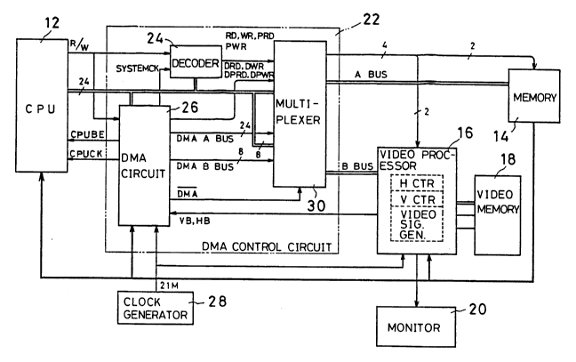
Referring to Figure 1, an image processing system
10 such as a TV game machine of this embodiment shown
includes a CPU 12 which provides overall control on the
components of the image processing device 10 including
a video processor 16 in accordance with a program
stored in a memory 14 in advance. For example, the CPU
12 may be a 16-bit microprocessor.
The video processor 16 reads graphic data from a
video memory 18 according to the instructions from the
microprocessor or CPU 12. The video processor 16 then
sends the graphic data to a monitor 20 through a TV
interface, not shown.
The memory 14 includes a working RAM and a program
data storage contained in a detachable memory
cartridge, not shown. The video memory 18 stores
-- 10 --
204991A
graphic data (dot data) about objects (i.e., characters
graphically moved by operator or by player) and about
background patterns (i.e., still images not moved by
operator or by player). The video processor 16
contains an H counter, a V counter and a video signal
generating circuit. The H counter forms one horizontal
scanning period by counting the number of dots in a
horizontal direction on the monitor 20, while the V
counter forms one vertical scanning period by counting
horizontal scanning lines on the monitor 20. The video
signal generating circuit, controlled by the CPU 12
according to the program data, reads the dot data for
necessary characters from the video memory 18.
A direct memory access (DMA) control circuit 22 is
also provided. In this embodiment, DMA operations are
carried out between the memory 14 and the video
processor 16 under control of the DMA control circuit
22.
The DMA control circuit 22 includes a decoder 24.
The decoder 24 supplies write and read signals to the
memory 14 and video processor 16 in accordance with a
signal R/W and an address signal on the address bus
from the CPU 12, and a system clock signal SYSTEMCK
from a DMA circuit 26, at a time when an operation
other than the DMA is performed. As will be described
2099911
later in detail, the DMA circuit 26 performs DMA data
transfer between the memory 14 and the video processor
16 as per instructions from the CPU 12 and or a timing
signal from the video processor 16. In this
embodiment, the DMA circuit 26 generates a system clock
signal SYSTEMCK for synchronizing the entire system as
well as a CPU clock signal CPUCK illustratively on the
basis of a basic clock signal of 21.47727 MHz from a
clock generator 28.
A multiplexer 30 supplies the memory 14 and the
video processor 16 with address data from the CPU 12
and with a control signal from the decoder 24 during a
normal operation. During the DMA operation, the
multiplexer 30 supplies the memory 14 and the video
processor 16 with address data and a control signal
from the DMA circuit 26. This embodiment uses a tri-
state buffer to switch between an A bus and the control
signal. The multiplexer 30 is only used to switch to a
B bus.
How the DMA control circuit 22 of Figure 1
performs a DMA operation is outlined below with
reference to Figure 2. This embodiment is constructed
to carry out selectively one of two kinds of DMA
operation, a general DMA and an H-DMA. The general DMA
operation involves starting data transfer in response
204991~
to a command from the CPU 12, and the H-DMA operation
concerns executing data transfer during each horizontal
blanking period. For these kinds of DMA operation, up
to eight channels (0-7) may be set concurrently.
Either the general DMA or the H-DMA operation is
performed selectively on each of the channels. The
general DMA operation is carried out as needed in
response to the commands from the CPU 12. As shown in
Figure 2, the H-DMA operation involves an H-DMA table
processing V performed immediately after a start of a
display period, an H-DMA data processing effected
immediately after a start of horizontal blanking and an
H-DMA table processing H executed immediately after the
H-DMA data processing. In the H-DMA table processing
V, the CPU 12 writes various parameters such as a
direction of transfer, an addressing mode, a B buss
mode, and etc. to a set parameter area in a DMA working
memory 502 (Figure 3A and Figure 29; to be described
later). The writing of the parameters is performed
prior to the data transfer in the H-DMA data
processing to be carried out immediately after entry
into a horizontal blanking period. In the H-DMA table
processing H, a line counting work area ~to be
described later) in the DMA working memory is
decremented, and the processing is performed according
- 13 -
20~991~1
to the decremented result.
Referring now to Figures 3A and 3B, the DMA
circuit 26 shown in Figure 1 is described below in
detail. The DMA circuit 26 contains a DMA timing
signal generating circuit 32. As illustrated in Figure
4, the DMA timing signal generating circuit 32
comprises a basic signal generating circuit 34, a
counter circuit 36, a data switching control signal
generating circuit 38, a channel ending circuit 40, an
arithmetic control circuit 42 and an LBO signal
generating circuit 44. The basic signal generating
circuit 34 generates basic timing signals VOHO, VDTOP,
lOM, /lOM, 5M, /5M, DMACK, /DMACK and MCK in accordance
with a basic clock signal 21M from the clock generator
28 (Figure 1) and with a horizontal blanking signal HB
and a vertical blanking signal VB from the video
processor 16. In this specification, a slash (/)
prefixed to a signal name means inversion.
As depicted in Figure 5, the basic signal
generating circuit 34 comprises a three-bit counter 46.
The counter 46 admits as its count input the basic
clock signal 21M, and as its reset signal a system
reset signal /RST from the CPU 12. The counter 46
frequency-divides the basic clock signal 21M by two to
output the signals lOM and /lOM. The signal lOM is
- 14 -
204991'1
frequency-divided furthér by two, whereby the signals
5M and /5M are generated. One cycle of the signal 5M
corresponds to a display period of one dot (pixel) on
the monitor 20. The clock signal DMACK, which serves
as the basic clock signal of the DMA operation, is
obtained by further frequency-dividing the signal 5M by
two. The signal /5M is fed as a clock input to D flip-
flops (DFF's) 48, 50, 52, 54 and 56 as well as to a
nine-bit counter 58. A D input of the DFF 48 is
supplied with the horizontal blanking period HB, and a
D input of the DFF 52 is supplied with the vertical
blanking signal VB. An output Q of the DFF 48 is
applied both to a D input of the DFF 50 and to one
input of an OR gate 60. An output /Q of the DFF 50 is
applied to the other input of the OR gate 60. Both an
output of the OR gate 60 and the system reset signal
/RST are fed to an AND gate 62. An output of the AND
gate 62 is supplied to a reset input /R of the nine-bit
counter 58. A count-up output of the nine-bit counter
58 is sent to the DFF 56 as a clock signal of the
latter. An output Q of the DFF 52 is applied as D
inputs to both DFF's 54 and 56, respectively. The
output Q of the DFF 52 is also applied to one of the
two inputs of each of NOR gates 64 and 66. An output
of the DFF 54 is fed to the other input of the NOR gate
20~9914
64, while an output /Q of the DFF 56 is supplied to the
other input of the NOR gate 66. The NOR gate 64
outputs the signal VOH0. The signal VOH0 is brought
High, as shown in Figure 35A, during one cycle period
of the signal /5M at the start of the above-described
display period of Figure 2. The NOR gate 66 outputs
the signal VDTOP. The signal VDTOP is also brought
High, as depicted in Figure 35A, during the display
period (i.e., scanning period) following the vertical
blanking period of Figure 2. The signal VDTOP going
High means that the H-DMA table processing V of Figure
2 is in effect.
The basic signal generating circuit 34 shown in
Figure 5 further comprises an eight-bit shift register
68. The shift register 68 admits the basic clock
signal 21M as its shift clock signal. A clear terminal
of the shift register 68 is supplied with the system
reset signal /RST. An address decoder 70 is also
provided to receive address data from the address bus.
According to the address data given, the address
decoder 70 outputs one of signals 3.58EN, 2.68EN and
1.79EN by which to set to one of three frequencies 3.58
MHz, 2.68 MHz and 1.79 MHz the clock signal MCK output
by the shift register 68. The signals 3.58EN, 2.68EN
and 1.7gEN are supplied to respective D inputs of DFF's
- 16 -
20~9914
72. Three outputs of the DFF's 72 are sent
respectively through an inverter 74, a NAND gate 76 and
a NAND gate 78 to a NAND gate 80. That is, the signal
3.58EN from the address decoder 70 is passed through
the DFF's 72 and inverted by the inverter 74 before
reaching one of inputs of the NAND gate 80. The output
Q of the DFF's 72 which corresponds to the signal
2.68EN is fed to one of two inputs of the NAND gate 76.
The other input of the NAND gate 76 is supplied with a
bit output QE from the shift register 68. The signal
QE is also applied to one of inputs of the NAND gate
78. The output Q of the DFF's 72 which corresponds to
the signal 1.79EN is sent to another input of the NAND
gate 78. The NAND gate 78 further receives a bit
output QG from the shift register 68 and an output Q
from a DFF 82. Outputs of the NAND gates 76 and 78 are
each inverted before being applied to the NAND gate 80.
An output of the NAND gate 80, together with a bit
output QC of the shift register 68, is fed to a NAND
gate 84. In turn, An output of th~ NAND gate 84 is
supplied to an input SI of the shift register 68. The
DFF 82 admits the basic clock signal 21M as its clock
signal, a bit output QH of the shift register 68 as its
D input, and the system reset signal /RST as its reset
input /R. ~y frequency-dividing the basic clock signal
20~g91~
2lM, the shift register 68 outputs the clock signal MCK
from its bit output QB. The clock signal MCK provides
the basis for generating the system clock signal
SYSTEMCK. It is to be noted that during a DMA
operation, changes in the frequency of the signal MCK
have no significance because the clock signal DMACK, to
be described later, is used as the system clock signal.
As shown in Figure 6, the counter circuit 36
contains a six-bit shift register 86. The shift
register 86 receives the signal /lOM as its shift clock
signal. A D input of a DFF 88 and one of the inputs of
an AND gate 90 are supplied with a signal RACK. The
signal RACK is generated by a DAM start/stop circuit
206, to be described later (Figure 3 (B), Figures 13 -
18) in starting the DMA, in switching channels, or intransition from H-DMA data processing to H-DMA table
processing H. The DFF 88 receives the signal /lOM as
its clock signal. An output /Q of the DFF 88 is
applied to the other input of the AND gate 90. Thus,
at a leading edge of the signal RACK, the AND gate 90
outputs a signal LCNT that is brought High during one
cycle of the signal /lOM. The signal LCNT serves as a
pulse signal by which to detect leading edges of the
signal RACK. The shift register 86 receives the signal
LCNT as its input. After the signal LC~T is brought
- 18 -
204991~
High, the shift register 86 consecutively outputs
timing signals SHT0 - SHT5 from its outputs D0 - D5
during each cycle of the signal /lOM. The timing
signal SHT0 is obtained by delaying the signal LCNT by
one cycle of the signal 10M. Likewise, the timing
signal SHT5 is acquired by delaying the signal LCNT by
six cycles of the signal 10M.
The signal SHT0 from the shift register 86 is
inverted by an inverter 92 before being fed to one of
three inputs of an AND gate 94. The other two inputs
of the AND gate 94 are supplied with the system reset
signal /RST and an output of a NAND gate 96. The NAND
gate 96 is a four-input NAND gate receives a signal
GDMA that goes High upon the general DMA operation
triggered by the DMA start/stop circuit 206, to be
described later (Figure 3B) and indicates that the
general DMA operation is in effect, the clock signal 5M
and and a clock signal DMAC from the basic signal
generating circuit 34 (Figure 5), and an output Q of a
DFF 98, i.e., a signal PAIREND. The signal PAIREND
indicates that the H-DMA data processing has ended on
one channel. An output of the NOR gate 94 is sent to
the reset input /R of a two-bit counter 100. The two-
bit counter 100 receives an output Q of a DFF 102 as
its clock input. The signal 10M is applied as a clock
-- 19 --
20 1391~
input to both the DFF 98 and the DFF 102. A D input of
the DFF 102 receives the signal DMACK. Thus, during H-
DMA table processing or general DMA operation, the two-
bit counter 100 is reset by the signal SHT0 from the
shift register 86. The two-bit counter 100 outputs
count data COUNT in the H-DMA processing. The count
data COUNT is reset by the signal PAIREND from the DFF
98 and counted up every four cycles of the signal 10M.
The count data COUNT, i.e., the signal from the
two-bit counter 100 is supplied to a ROM 104.
Meanwhile, the above-noted signal LCNT is inverted by
an inverter 106 before being applied to the clock input
of a DFF 108. A D input of the DFF 108 receives B bus
mode data (3-bit) from a set parameter register 584
(Figure 3B), to be described later. In accordance with
these inputs, the ROM 104 outputs signals BFAl, BFA0
and PE as listed in Table I below.
- 20 -
20~9914
Table I
B bus mode COUNT BFAl BFA0 PE
00 0 0
000 01 -- -- --
-- -- --
11 -- -- --
00 0 0 0
001 01 0
1 0
00 0 0 0
010 01 0 0
1 0
00 0 0 0
011 01 0 0 0
0 1 0
11 0
00 0 0 0
100 01 0 1 0
1 0 0
11 1 1 1
The data or signals BFAl and BFA0 are fed, as an
augend each for the B bus data, to a B bus arithmetic
circuit 590 (Figure 3B). The signal PE is applied to a
D input of the DFF 98. Thus, during a general DMA
operation, the signal PE is used to reset the two-bit
counter 100. During the H-DMA data processing period,
the signal PE provides the basis for generating a
channel end signal DMACHEND. The above-described
signal PAIREND generated with the signal PE is supplied
to the DMA start/stop circuit 206, to be described
20~3914
later, as the timing signal by which to start the H-DMA
process while the general DMA is performed.
The data switching control signal generating
circuit 38 shown in Figure 7 contains a ROM 110. The
ROM 110 receives four bits of data, i.e., the clock
signals 5M and DMACK as well as the count data COUNT
from the counter circuit 36 (Figure 6). The ROM 110
outputs signals D0 and Dl as indicated in Table II
below.
Table II
COUNTDMACK 5M Dl D0
0 0
00 0 0 0 0
0 1 0
0 0
1 1 0 0
01 0 0 0 0
0
0
0 0
0 0 0 0
0
0
The outputs D0 and Dl from the ROM 110 are fed to
a D inputs of DFF's 112. Each of the DFF's 112
receives the signal /lOM as its clock signal. One of
the two outputs Q of the DFF's 112 is fed to one input
of an exclusive-OR gate 114 and the other output Q of
- 22 -
2049914
the DFF's 112 is given to one input of an exclusive-OR
gate 116. The other inputs of the exclusive-OR gates
114 and 116 are supplied with the output of an AND gate
118. The signal VDTOP and a signal LINE0 are given to
a latch 122. The signal LINE0 is outputted when the
result of operations by an arithmetic circuit 580
(Figure 3A), to be described later, becomes zero, i.e.,
when the number of lines in the work area reaches zero
during the H-DMA process. The latch 122 receives as
its latch signal the signal SHT0 from the counter
circuit 36 (Figure 6). An output of the latch 122 is
applied to a D input of the DFF 124. The DFF 124
receives the signal DMACK as its clock signal. An
output Q of the DFF 124, together with the signal SHT4
from the counter circuit 36, is applied to an input of
the above-described AND gate 118. An output of the
exclusive-OR gate 114 and an output of the exclusive-OR
gate 116 are fed, respectively, to one input of an AND
gate 126 and one input of an AND gate 128. The other
inputs of the AND gates 126 and 128 are commonly
supplied with a signal TABLE from the DMA start/stop
circuit 206, to be described later. The signal TABLE
is brought High during H-DMA table processing V and
during H-DMA table processing H. In this manner, the
AND gates 126 and 128 output signals DSEL0 and DSELl.
20~991 1
The signals DSEL0 and DSELl both become ~o n during the
general DMA operation and during the H-DMA data
processing period. During the H-DMA data processing
period, the signals DSEL0 and DSELl vary with the
output of the ROM 110. If the number of lines counted
by the arithmetic circuit 580, to be described later,
becomes zero during H-DMA table processing V or during
H-DMA table processing H, the exclusive-OR gates 114
and 116 trigger inversion of the output from the ROM
110, i.e., from the DFF 112. That is, the signals
DSELl and DSEL0 are changed from "0, 1" to "1, o n
This is equivalent to supplying the DMA working memory
502 (Figure 3A), to be described later, with the line
count data from the memory 14 (Figure 1) using the same
timing as the process of supplying the "line count
minus 1" to the DMA working memory 502.
The arithmetic control circuit 42 depicted in
Figure 8 comprises AND gates 130 and 132, an inverter
134 and an OR gate 136. In accordance with A bus
increment designation data D3 and D4 from the set
parameter register 584 (Figure 3B), to be described
later, the arithmetic control circuit 42y generates
signals XFAl and XFA0. The signals XFAl and XFA0 are
used to designate an arithmetic procedure "+1~, ll+0" or
r-l" for the arithmetic circuit 580 (Figure 3A).
- 24 -
`- 20~991~
- The LBO signal generating circuit 44 shown in
Figure 12 contains a DFF 138, a NOR gate 140 and an AND
gates 142. The LBO signal generating circuit 44
generates a signal LBO on the basis of the clock
S signals 10M and DMACK. The signal LBO is given as a
latch signal or a load signal to an A bus register 586
and a B bus register 592 (both in Figure 3B), to be
described later.
The channel ending circuit 40, whose details are
shown in Figure 10, comprises a general DMA channel
ending circuit 144, an H-DMA data processing channel
ending circuit 146 and an H-DMA table processing
channel ending circuit 148. One of signals GCEND,
DCEND and TCEND generated by these circuits is selected
by a data selector 150. The selected signal is
outputted as the signal DMACHEND indicating the end of
each channel.
As depicted in Figure 11, the general DMA channel
ending circuit 144 includes a NOR gate 152 that
receives through one of its inputs a signal /~ ND
from an end judging circuit 578 (Figure 3A), to be
described later. The signal /BYTEEND is outputted when
the result of operations by the arithmetic circuit 580
becomes zero, i.e., when the number of continuously
transmitted data during the general DMA operation
- 25 -
20~931~
becomes zero. An output of the NOR gate 152 is fed to
a D input of a DFF 154. In turn, an output of the DFF
154 is supplied through a DFF 156 to the other input of
the NOR gate 152. The DFF 154 receives as its clock
signal an output of an AND gate 158. The AND gate 158
in turn receives the clock signal /DMACK and the signal
DMA. An output of the AND gate 158 is fed as a clock
signal to a DFF 160. The DFF 156 receives the signal
DMACK as its clock signal. The output of an AND gate
168 is applied to a set input /S of the DFF 154 and to
a reset input/R of a DFF 166. Two inputs of the AND
gate 168 are supplied with a pulse signal /DAST and
with the system reset signal /RST. The pulse signal
/DAST is outputted by the DMA start/stop circuit 206
and is brought Low at the start of a DMA operation. An
output /Q of the DFF 166, together with an output Q of
the DFF 154, is fed to a NOR gate 170. In turn, the
NOR gate 170 outputs a channel end signal GCEND for the
general DMA operation in response to the signal
/BYl~N~.
The H-DMA data processing channel ending circuit
146 contains an AND gate, not shown, which receives the
clock signal /DMACK and the signal PE from the counter
circuit 36 of the DMA timing signal generating circuit
32, and outputs a channel end signal DCEND for H-DMA
- 26 -
20~39~1
data processing in response to the signal PE.
The H-DMA table processing channel ending circuit
148 illustrated in Figure 12 comprises a ROM 172 that
receives the clock signals 5M and DMACK as well as the
count data COUNT from the counter circuit 36. The ROM
172 effects its output, i.e., supplies a D input of a
DFF 174 therewith in accordance with Table III below.
Table III
COUNT DMACK 5M D
00 0 0
0 1 0
0 0
0
01 0 0 0
0 1 0
1 o o
0 0
0 1 0
0 0
The DFF 174 receives the signal /lOM as its clock
signal. An output Q of the DFF 174 is sent to one of
the inputs of an AND gate 176. The other input of the
AND gate 176 is supplied with an output of a NAND gate
178. Three inputs of the NAND gate 178 receive an
output Q of a DFF 180, an output of a latch 182 and an
output /Q of a DFF 184. A D input of the DFF 184 is
- 27 -
20~991~
fed with a signal TYPE which is outputted by the set
parameter register 584 (Figure 3B) and which indicates
a direct addressing mode when set to H O 1~ and an
indirect addressing mode when set to n 1 n . The DFF 184
receives as its clock signal the signal /LCNT from the
counter 36. The latch 182 admits the signal VDTOP from
the basic signal generating circuit 34 or the signal
LINE0 from the arithmetic circuit 580 (Figure 3A)
through an OR gate 186. As its latch signal, the latch
182 receives the signal LCNT from the counter circuit
36. A D input of the DFF 180 receives an output Q of
an RS-FF 188, and an S input of the RS-FF 188 is
supplied with the signal SHT0 from the counter circuit
36, and an R input of the RS-FF 188 admits an output of
an OR gate 190. One of the two inputs of the OR gate
190 admits the signal SHT3 from the counter 36 and the
other input of the OR gate 190 is supplied with the
system reset signal /RST after inversion by an inverter
192. The DFF 180 receives as its clock signal the
signal 10M from the basic signal generating circuit 34.
In this manner, the AND gate 176 of the H-DMA table
processing channel ending circuit 148 outputs a channel
end signal TCEND for H-DMA table processing. That is,
when that signal TYPE is N0~ which comes from the set
parameter register 584 and which indicates the type of
- 28 -
20~9914
addressing mode, the signal TCEND is outputted at the
start of the data COUNT of "10~ and, when the signal
TYPE is "1", the signal TCEND is outputted at the start
of the data COUNT of ~oo H ~
The signals GCEND, DCEND and TCEND output in the
manner described are applied to the data selector 150.
As its selection inputs, the data selector 150 receives
two outputs Q from DFF's 194, as shown in Figure 10.
Two D inputs of the DFF's 194 admit outputs of AND
gates 196 and 198. One input of the AND gate 196
receives a signal TABLETIM (providing the basis for
generating the signal TABLE) which comes from the DMA
start/stop signal 206 and which is inverted by an
inverter 200. The other input of the AND gate 196
admits an output of an AND gate 202. Two inputs of the
AND gate 198 are supplied with the signal TABLETIM and
with the output of the AND gate 202. The AND gate 202
is fed with a signal HDMASEL (providing the basis for
generating a signal HDMA) from the DMA start/stop
circuit 206 and with an output Q of a DFF 204 which
also admits the signal HDMASEL. As with the DFF's 194,
the DFF 204 receives the clock signal 5M from the basic
signal generating circuit 34. Two outputs Q of the
DFF's 194 are both "0~ during the general DMA
operation. In this state, the data selector 150
- 29 -
20~991~
outputs as the channel end signal DMACHEND the signal
GCEND from the general DMA channel ending circuit 144.
During the H-DMA data processing period, the inputs Sl
and S0 of the data selector 150 are "1, on. Thus the
data selector 150 outputs as the channel end signal
DMACHEND the signal DCEND from the H-DMA data
processing channel ending circuit 146 during the H-DMA
data processing period. During the H-DMA table
processing period, the inputs of the data selector 150,
i.e., the two outputs Q of the DFF's 194, are both "ln.
Thus, the data selector 150 outputs as the channel end
signal DMACHEND the signal TCEND from the H-DMA table
processing channel ending circuit 148 during the H-DMA
table processing period.
Referring now to Figures 13 through 18, the DMA
start/stop circuit 206 shown in Figures 3B will be
described below. As illustrated in Figure 13, the DMA
start/stop circuit 206 comprises an H-DMA start/stop
circuit 208, a general DMA start/stop circuit 210, a
system control signal generating circuit 212 and a
start signal generating circuit 214.
The H-DMA start/stop circuit 208 includes an H-DMA
timing control circuit 216 (whose details are given in
Figure 15), as depicted in Figure 14. The H-DMA
start/stop circuit 208 of Figure 14 contains DFF's 218,
- 30 -
2049914
220 and 222 connected in a cascade fashion. A D input
of the DFF 218 admits an output of an AND gate 224.
Two inputs of the AND gate 224 are supplied with a
signal /HDMAEND indicating an end of H-DMA and with a
signal HEN from a start enable circuit in a priority
judging circuit 382 (Figure 3A, Figures 19 - 24), to be
described later. The DFF's 218, 220 and 222 receive
the clock signal /lOM from the basic signal generating
circuit 34. An output Q of the DFF 222 is applied as a
signal /HDMASTP to reset inputs /R of DFF's 226 and
228. A D input of the DFF 226 is set to "1~ and the
clock signal sent thereto is an output of an AND gate
230. One input of the AND gate 230 admits a signal
/NOHDMA from the start enable circuit to be described
later and the other input of the AND gate 230 is
supplied with the signal VDTOP from the basic signal
generating circuit 34 and with an output of an OR gate
232 that receives an output of an AND gate 234. The
AND gate 234 admits the blanking signals VB and HB from
the video processor 16 (Figure 1) while the blanking
signal VB is inverted by an inverter 236. Thus in
accordance with the horizontal blanking signal HB or
the signal VDTOP, the AND gate 230 outputs a trigger
signal for stating the H-DMA only when the signal
/NOHDMA that comes from the start enable circuit 392
- 31 -
20~9914
(Figure 24) in the priority judging circuit 382 is
High. The signal GDMA from the general DMA start/stop
circuit 210 is sent to one input of an AND gate 238 as
well as to one input of an AND gate 240, the signal
GDMA being inverted by an inverter 242 before reaching
the AND gate 238. The other input of the AND gate 238
admits an output of the AND gate 230. Remaining two
inputs of the AND gate 240 are fed with an output Q of
the DFF 226 and with an output Q of the DFF 244. A D
input of the DFF 244 receives the signal /PAIREND from
the DMA timing signal generating circuit 32, and a
clock signal applied to the DFF 244 is the signal /lOM.
The AND gate 238 outputs a signal DHDMA to the H-DMA
timing control circuit 216 whose details are shown in
Figure 15.
The H-DMA timing control circuit 216 comprises
DFF's 246, 248, 250, 252, 254, 256, 258, 260, 262 and
264, an OR gate 266, an AND gate 268 and a NOR gate
270. The H-DMA timing control circuit 216 receives the
signal DHDMA from the AND gate 238 (Figure 14), the
signal /HDMASTP and the signal HEN, and outputs signals
SCKENH, /CPUCKENH and DHDMADL.
The signal DHDMADL from the H-DMA timing control
circuit 216 is supplied, together with an output of the
AND gate 240 (Figure 14), to an OR gate 272. An output
2~991q
of the OR gate 272 is applied to a D input of a DFF
274. An output Q of the DFF 274 is applied as a clock
signal to the DFF 228. An output Q of the DFF 228 is
outputted as a signal HDMA that is brought High during
the H-DMA operation. The signal HDMA is also applied
as a clock signal to a DFF 276. The DFF 276 receives
an output of the NOR gate 224 to its reset input /R.
An output Q of the DFF 276 is provided as the signal
HDMASEL.
The general DMA start/stop circuit 210, whose
details are depicted in Figure 16, comprises an AND
gate 280 that receives a signal from a general DMA
timing control circuit 278. The general DMA timing
control circuit 278 includes DFF's 282, 284, 286, 288,
290, 292, 294 and 296, an OR gate 298 and a NOR gate
300. The general DMA timing control circuit 278
receives a signal /NOGDMA from the start enable circuit
392 (Figure 24) and the system reset signal /RST, and
outputs signals SCKENG, CPUCKENG and GDMADL. An output
Q Of the DFF 282 is applied, together with the system
reset signal /RST, to the AND gate 280. In turn, an
output of the AND gate 280 is fed to a reset input /R
of a DFF 302. The DFF 302 receives as its clock signal
an output Q of a DFF 304. A D input of the DFF 304 is
supplied with the signal GDMADL from the general DMA
- 33 -
2049914
timing control circuit 278, i.e., an output Q of the
DFF 296. An output Q of the DFF 302 is obtained as a
signal GDMAPR and is applied to one of two inputs of an
AND gate 306. The other input of the AND gate 306 is
fed with an output of an inverter 308 that receives the
signal HDMA from the H-DMA start/stop circuit 208
(Figure 14). Thus the AND gate 306 outputs the signal
GDMA that goes High during the general DMA operation.
The system control signal generating circuit 212,
whose details are illustrated in Figure 17, comprises
an AND gate 310 that receives the clock signal MCK, the
signal SCKENH from the H-DMA timing control circuit 216
and a signal SCKENG from a general DMA timing control
circuit 278. An output of the AND gate 310 is applied
to one of two inputs of an OR gate 312. The other
input of the OR gate 312 is supplied with an output of
an AND gate 314. The AND gate 314 receives the signal
DMA which is brought High during the DMA operation
period, the clock signal DMACK from the basic signal
generating circuit 34, and an output Q of a DFF 316. A
D input of the DFF 316 receives an output of a NOR gate
318. The clock signal /DMACK and the signal DMA are
applied to an AND gate 320. In turn, an output of the
AND gate 320 is supplied as a clock signal to DFF's 322
and 324. A D input of the DFF 322 receives an output
- 34 -
204991 1
of a NOR gate 326 that admits the signal /~ N~ and
an output of a DFF 328. An output Q of the DFF 322 is
applied to one of two inputs of an AND gate 330 as well
as to a D input of the DFF 328. The DFF 328 receives
the clock signal DMACK. An output of an AND gate 332
that receives the signal /DAST and the system reset
signal /RST is supplied to a set input /S of the DFF
322 as well as to a reset input /R of the DFF 324. The
signal GDMA from the general DMA start/stop circuit 210
(Figure 16) enters the other input of the AND gate 330.
An output of the AND gate 330 is applied, together with
an output Q of the DFF 324, to the NOR gate 318. The
DFF 316 receives the signal 10M as its clock signal.
Thus an output of the DFF 316 is applied as a /CKdrop
to the AND gate 314. This causes the system clock
signal SYSTEMCK to drop one clock cycle when the signal
/BYTEEND is brought Low immediately after the start of
DMA or during the general DMA operation. In this
manner, write and read signals in a DMA control signal
generating circuit 562 (Figure 3A and Figure 32) are
disabled during one clock cycle, respectively.
The system control signal generating circuit 212
further comprises an OR gate 334. The OR gate 334
receives the clock signal MCK, the /CPUCKENH from the
H-DMA start/stop circuit 208 and the signal /CPUCKENG
204991~
from the general DMA start/stop circuit 210. An output
of the OR gate 334 is applied as the CPU clock signal
CPUCK to the CPU 12 (Figure 1). The system control
signal generating circuit 212 also includes a NOR gate
336 whose two inputs admit the signals DHDMADL and
GDMADL. An output of the NOR gate 336 is inverted by
an inverter 338 before being applied to the CPU 12 as a
CPU bus enable signal /CPUBE. When the signal /CPUBE
remains Low, that means the CPU 12 is outputting
address data.
The start signal generating circuit 214, details
of which are shown in Figure 18, contains an OR gate
340 that receives the signal HDMA from the H-DMA
start/stop circuit 208 and the signal GDMA from the
general DMA start/stop circuit 210. An output of the
OR gate 340 is the signal DMA that goes High during the
DMA operation period. An output of a NOR gate 342 that
receives the system reset signal /RST and signals /RAST
and /TAST is outputted as a signal /TRES and is applied
to one of two inputs of an AND gate 344. The other
input of the AND gate 344 receives the channel end
signal DMACHEND that has passed through an inverter
346. The AND gate 344 outputs the signal RACK
described earlier.
The start signal generating circuit 214
- 36 -
2o~99l l
additionally includes DFF's 348 and 350 whose inputs
are fed with the signals HDMASEL and GDMA. The DFF's
348 and 350 commonly receive the clock signal DMACK.
An output of the DFF 348 is supplied, together with the
signal HDMASEL, to a NAND gate 352. An output Q of the
DFF 350 is applied, together with the signal GDMA, to a
NAND gate 354. An output of the NAND gate 352 and an
output of the NAND gate 354 are both fed to an AND gate
356. In turn, an output of the AND gate 356 provides
the above-mentioned signal /DAST.
A D input of a DFF 358 admits a signal EO that is
brought Low at the end of the DMA operation. The DFF
358 receives the signal /lOM as its clock signal. An
output Q of the DFF 358 is supplied to one of two
inputs of an OR gate 360. The other input of the OR
gate 360 receives an output of a NOR gate 362 which in
turn admits the signal /DAST and an output Q of a DFF
364. A D input of the DFF 364 is fed with the signal
/DAST, and a clock signal applied to the DFF 364 is the
signal /lOM. An output of the NOR gate 362 is inverted
by an inverter 366 before reaching a reset input /R of
a DFF 368. A D input of the DFF 368 is N1", and the
DFF 368 receives as its clock signal an output of an OR
gate 370. The OR gate 370 is supplied both with an
output of the OR gate 360 and with an output Q of a DFF
- 37 -
204991~
372. The DFF 372 receives the signal 10M as its clock
signal, and a D input of the DFF 372 admits an output
of the OR gate 360. An output Q of the DFF 368 is
outputted as the signal TABLETIM, and is applied to one
of two inputs of an OR gate 374 and to a D input of a
DFF 376. An output /Q of the DFF 368 is fed to one of
two inputs of an OR gate 378. The other inputs of the
OR gates 374 and 378 are supplied with an output of the
OR gate 370. The OR gate 374 provides the signal
/TAST, and the OR gate 378 outputs the signal /HDMAEND.
The DFF 376 receives the signal 5M as its clock signal.
An output of the DFF 376 is applied, together with the
signal HDMA, to an AND gate 380. In turn, the AND gate
380 provides the signal TABLE that is brought High
during the H-DMA table processing period.
The signal /DAST is a pulse signal that goes Low
at the start of the DMA operation, while the signal
/TAST is a pulse signal that is brought Low when the H-
DMA table processing period begins. The signal
TABLETIM provides the basis for generating the signal
TABLE. The signal /HDMAEND is brought Low at the end
of the H-DMA processing period. The signal /RACK is
outputted when a applied channel is activated. In
response to the signal /RACK, setting a mode and
initialization of the entire DMA circuit 26 are
- 38 -
20~991~
performed. The signals DMA, /DAST and /TRES are
outputted at the start of the DMA operation, and the
signals TABLE, TABLETIM and /TAST are outputted when H-
DMA table processing is started.
Referring now to Figures 19 through 24, the
priority judging circuit 382 (Figure 3A) is described
below. The priority judging circuit 382 comprises a
status storing/selecting circuit 384, a status storage
control circuit 386, a priority circuit 388, an
interrupting circuit 390 and the start enable circuit
392.
Details of the status storing/selecting circuit
384 are depicted in Figure 20. The status
storing/selecting circuit 384 contains a DFF 392 that
latches data END as per the clock signal DMACK. An
output of the DFF 392 is supplied via a gate circuit
394 to an intra-frame operation enable register 396.
The intra-frame operation enable register 396 comprises
eight RS-FF's. A reset input R of each of the RS-FF's
receives each bit output of the gate circuit 394 and a
set input S of each RS-FF admits the signal VOH0. The
signal V0H0 is applied through an inverter 398 to a
reset input /R of the DFF 392. The gate circuit 394
contains eight NOR gates. One of the two inputs of
each AND gate in the gate circuit 394 receives one of
- 39 -
2049914
outputs Q0 - Q7 from the DFF 392, respectively. The
other input of each AND gate in the circuit 394 admits
a signal /LITIM. The signal /LITIM is outputted when
the line count data loaded from the memory 14 is zero.
Thus the intra-frame operation enable register 396 is
reset with the signal /LITIM, thereby to disable a
current channel until a next frame. The outputs of the
intra-frame operation enable register 396 are supplied,
through a gate circuit 400 comprising eight AND gates,
to a gate circuit 402 and are also outputted as data
HDMAEN0-7.
One of two inputs of each AND gate in the gate
circuit 400 receives each bit output from the intra-
frame operation enable register 396. The other input
of each AND gate in the gate circuit 400 admits each of
bits constituting data HDMAEN0-7. A gate circuit 404
comprising eight NOR gates receives bit outputs from
the DFF 392. A signal PATH is fed to the gate circuit
404 whose outputs are applied to a data transfer enable
register 406. The data transfer enable register 406
contains eight RS-FF's whose reset inputs R admit bit
outputs from the gate circuit 404. Set inputs S of the
data transfer enable register 406 are supplied with the
signal /TAST. In response to a signal /PATH, the gate
circuit 404 outputs data that corresponds to the
- 40 -
20~991~
current channel number. The output data enters reset
inputs R of the data transfer enable register 406 so
that when a data transfer mode is "0", data transfer is
disabled during a next horizontal blanking period.
Outputs of the data transfer enable register 406 are
applied to the other input of each RS-FF in the gate
circuit 402. Outputs of the gate circuit 402 are fed
to a data selector 408 which receives the signal
HDMASEL as its selection input. Thus during the H-DMA
or general DMA operation, the data selector 408 outputs
enable signals DEN0-DEN7 corresponding to each channel.
The enable signals DEN0-DEN7 are sent to the priority
circuit 388 (Figure 19).
The status storage control circuit 386,
illustrated in detail in Figure 21, generates the
signals /LITIM and /PATH which are applied to the
status storing/selecting circuit 384 (Figure 20). The
status storage control circuit 386 comprises an OR gate
410 that receives the signal /VDTOP from the basic
signal generating circuit 34 and the signal LINE0. An
output of the OR gate 410 is latched by a latch 412 in
response to the signal SHT0. An output of the latch
412 enters a D input of a DFF 414. The DFF 414 admits
the clock signal DMACK. An output Q of the DFF 414 is
applied to one input of an AND gate 416, and an output
- 41 -
204991~
/Q of the DFF 414 is sent to one input of an AND gate
418. Remaining two inputs of the AND gate 416 receive
Q outputs of DFF's 420 and 422. A D input of the DFF
420 admits the signal SHT5, and the DFF 420 receives
the clock signal 10M. D D input of the DFF 422 is fed
with an output of an AND gate 424 that receives both
the signal TABLE and a signal TBEND. As its clock
signal, the DFF 422 admits the signal SHT4 through an
inverter 426. Thus the AND gate 416 outputs the signal
LITIM when the signal TBEND from the end judging
circuit 578 is brought High with a predetermined timing
(of signal SHT4), i.e., when the data bus value becomes
zero. The signal LITIM is inverted by an inverter 428,
and an inverted signal /LITIM is sent as a control
signal to the gate circuit 3~4 of Figure 20.
Remaining two inputs of the AND gate 418 that
receives an output /Q of the DFF 414 are supplied with
a signal C via an inverter 430 and with an output Q of
a DFF 432. A D input of the DFF 432 receives the
signal SHT3, and the DFF 432 admits the signal 10M as
its clock signal. An output of the AND gate 418 is
applied, together with the signal TABLE, to an AND gate
434. An output of the AND gate 434 is fed to one of
the two inputs of a NOR gate 436. The other input of
the NOR gate 436 receives the signal VOH0. Thus the
- 42 -
204391 i
NOR gate 436 outputs the signal /PATH when the most
significant bit in a line register of a data switching
circuit is brought Low at a specific timing. The
signal /PATH is applied as a control signal to the gate
circuit 404 shown in Figure 20.
The priority circuit 388, details of which are
depicted in Figure 22, comprises a channel register 438
that is reset by the signal /TRES. Channel data
CHNLR0-7, after leaving the channel register 438, enter
a gate circuit 440 that contains eight NAND gates. The
gate circuit 440 receives as its gate signal the signal
DEN0-DEN7 from the data selector 408 for the status
storing/selecting circuit 384 shown in Figure 20. An
output of the gate circuit 440 is applied to a priority
encoder 442. The priority encoder 442 outputs signals
for carrying-out the DMA operations on channels 0
through 7, in that order, the signals being fed to a
DFF 444. When all channels have been finished, the
priority encoder 442 outputs the signal EO after
bringing it Low. Register number data REGNO, which was
latched with the signal RACK in the DFF 444, is
forwarded to a decoder 446. The decoder 446 decodes
supplied data REGNO and outputs one of enable signals
ENDOX through END7X for each channel. The enable
signal thus outputted enters a gate circuit 448 which
20~3~14
in turn outputs a general DMA register reset signal
/GRREAS0-7. This reset signal passes through an
inverter 450 and is applied as a clock signal to the
DFF's that constitute the above-described channel
register 438. In this manner, the priority circuit 388
resets the channel register 438 in response to the
signal /TRES from the DMA start/stop circuit 206 during
the H-DMA operation. Thus DMA operations are performed
consecutively on the channels 0 through 7, in that
order. The number of the currently operating channel
is applied as the address to a DMA working memory, to
be described later. When all channels have been
finished, the signal EO is brought Low and the current
H-DMA operation is stopped. Every time a general DMA
operation ends on a applied channel, a reset signal
/GRRES corresponding to that channel is outputted. The
reset signal is supplied as a reset signal to a general
DMA register 574 (Figure 3A), to be described later.
As in the H-DMA operation, the number of the currently
operating channel is applied as the address to the DMA
working memory 502.
The interrupting circuit 390 shown in Figure 23
contains a DFF 452. The DFF 452 receives as its data
input each of bits of data REGNO0-2 from the DFF 444 in
the priority circuit 388 of Figure 22. As its clock,
204931~
the DFF 452 admits the signal DMACK. An output of the
DFF 452 and the data REGNO0-2 are supplied to inputs of
a data selector 454. The signal /SHT0 from the counter
36 is applied as a selection signal S to the data
selector 454. Thus in response to the signal /SHT0
from the DMA timing signal generating circuit 32, the
interrupting circuit 390 forwards the number of the
preceding channel as an address signal to a switching
circuit 550 (Figure 3A), to be described later. This
makes possible the transition from one channel to the
next without time loss. For example, in Figure 35B, an
address value for the DMA working memory ~Figure 3A)
changes from "0013" to N0033", "0233", and "4257".
High-order three bits indicate the number of the
currently operating channel. This means that following
"4n, every numeral should be 4 or higher. However,
time losses occur in such cases as "0233", n-2--~ and
"4-57" where each dash (-) indicates a loss. In cases
such as "0233" and "4257", the flow of data over the
data bus fails to keep up with the operation. Thus one
way to go back on the channel number by one with a
specific timing is to provide an optimal timing.
The start enable circuit 392 illustrated in Figure
24 comprises three OR gates 456, 458 and 460. The OR
gate 456 receives the signal HDMAON0-7 from the status
- 45 -
20~9911
storing/selecting circuit 384 in Figure 20, and the NOR
gate 458 admits data GDMAEN0-7 from a general DMA
register, to be described later, and the NOR gate 460
accepts data HDMAEN0-7 from an H-DMA register, to be
described later. Thus when at least one H-DMA channel
is enabled, the NOR gate 456 outputs a high level
signal /NOHDMA. When at least one channel of the
general DMA register is enabled, the NOR gate 458
outputs a high level signal /NOGDMA. When all outputs
from the H-DMA register 572 tFigure 3A), to be
described later, are brought Low, the NOR gate 460
outputs a low level signal HEN. The signal /NOHDMA
serves as an H-DMA start signal and the signal /NOGDMA
as a general DMA start signal. The signal HEN acts as
an H-DMA stop signal.
Referring to Figures 25 through 28, a DMA address
generating circuit 462 (Figure 3A) is described below.
The DMA address generating circuit 462 comprises a
general DMA address generating circuit 464, an H-DMA
table processing address generating circuit 466 and an
H-DMA data processing address generating circuit 468.
Any of the data GA0,1; TA0,1 and DAD0,1 respectively
from the circuits 464, 466 and 468 is selected by a
data selector 470 and fed to a switching circuit 500
(Figure 3A), to be described later.
- 46 -
2049914
Figure 26 shows details of the general DMA address
generating circuit 464. The general DMA address
generating circuit 464 includes an AND gate 472. One
input of the AND gate 472 receives the signal DMA and
the other input thereof admits the clock signal /DMACK.
An output of the AND gate 472 is applied as a clock
signal to a DFF 474. A D input of the DFF 474 is fed
with an output of a NOR gate 476. The NOR gate 476
admits the signal /BY~ N~ and an output Q of a DFF
478. A D input of the DFF 478 receives an output Q of
the DFF 474. An output of the AND gate 472 is also
applied as a clock signal to the DFF 478. A set input
/S of the DFF 474 admits an output of an AND gate 480.
The AND gate 480 is supplied with the signal /DAST and
with the system reset signal /RST. An output of the
DFF 474 is applied to one input of a NOR gate 482 and
to one input of a NOR gate 484. The other input of the
NOR gate 482 receives the clock signal /DMACK, and the
other input of the NOR gate 484 admits the clock
signal DMACK. Thus the NOR gates 482 and 484 output
address data GAl and GA0 which become "0" when the
signal /DAST is received from the DMA start/stop
circuit 206 or when the signal /BYTEEND is admitted
from the end judging circuit 578 (Figure 3A).
Otherwise the address data GA and GA0 are alternately
- 47 -
20~991-1
set to "1" and "2" and vice versa in synchronous with
the clock signal DMACK.
The H-DMA table processing address generating
circuit 466, details of which are illustrated in Figure
27, contains a ROM 486. The ROM 486 receives the clock
signals 5M and DMACK as well as the count data COUNT,
and outputs D0 and Dl as per Table IV below.
Table IV
COUNT DMACK 5M Dl D0
00 0 0
0 1 0 0
0 0 0
01 0 0
0 1 0 0
0 1 0
0 0
0 1 0 0
0 1 0
An output of the ROM 486 is applied to a D input
of a DFF 488. The DFF 488 receives the signal /lOM as
its clock signal. An output Q of the DFF 488 is
outputted as the address TA0 and an output /Q thereof
is input to an AND gate 490. The AND gate 490 also
receives an output of a NAND gate 492. The NAND gate
492 admits both the signal VDTOP and the signal SHTl.
- 48 -
20~9914
- An output of the AND gate 490 becomes address TAl. In
this manner, the H-DMA table processing address
generating circuit 466 generates the addresses TA0 and
TAl for H-DMA table processing. Only during the H-DMA
table processing V shown in Figure 2 does the ROM 486
output "3~ using the timing: COUNT = 00, DMACK = 1, 5M
= 1. Then the output of the ROM 486 is latched by the
DFF 488 with the next timing: COUNT = 00, DMACK = 0, 5M
= 0. At this point, the data TA0 and TAl are changed to
10 "1" .
The H-DMA data processing address generating
circuit 468, details of which are shown in Figure 28,
includes a DFF 494 and an AND gate 496. A D input of
the DFF 494 is supplied with the signal TYPE via an
inverter 498, and the DFF 494 receives the signal LCNT
as its clock signal. An output Q of the DFF 494 is
sent to one input of an AND gate 496 and the other
input thereof admits the signal /LCNT. The H-DMA data
processing address generating circuit 468 provides
address data DA0 and DAl for the H-DMA data processing
depicted in Figure 2. Only upon receipt of the signal
/LCNT from the DMA timing signal generating circuit 32,
do the output address data become "3". Otherwise the
output data DA0 and DAl become "3" when the addressing
mode signal TYPE from the set parameter register
- 49 -
204991 1
(described later) is Low and the data become ~2" when
the signal TYPE is High.
In the manner described, the data selector 470
selects any of the address data output by the general
DMA address generating circuit 464, the H-DMA table
processing address generating circuit 466 and the H-DMA
data processing address generating circuit 468. The
selected address data is sent to the switching circuit
500 (Figure 3A) as low-order two bits of the address of
the DMA working memory 502 (Figure 3A).
Selection signals to the data selector 470 come
from AND gates 504 and 506. Two inputs of the AND gate
504 are fed with the signal HDMA that goes High during
the H-DMA operation period and with the signal TABLE
that is brought High during the H-DMA table processing
period. One input of the AND gate 506 receives the
signal HDMA and the other input thereof admits the
signal TABLE after inversion by an inverter 508. This
means that during the general DMA operation period,
outputs of the AND gates 504 and 506 are both brought
Low. During that period, the data selector 470 selects
as address DREGAD0-1 data GA0-1 from the general DMA
address generating circuit 464. During the HDMA table
processing period, either the AND gate 504 or the AND
gate 506 provides a high level output. In that case,
- 50 -
201991~
the data selector 470 selects the address TA0-1 from
the H-DMA table processing address generating circuit
466. During the H-DMA data processing period, the AND
gate 504 provides a high level output while the AND
gate 506 yields a low level output. This causes the
data selector 470 to select the data DAD0-1 from the H-
DMA data processing address generating circuit 468.
As illustrated in Figure 29, the DMA working
memory 502 comprises a high-order working memory 510a,
a middle-order working memory 510b and a low-order
working memory 510c. The working memories 510a, 510b
and 510c each contain a memory area of 32 bits by 8
bits in size. The DMA working memory 502 is a memory
for storing various settings to execute the DMA
operations. The signal /CPUBE and the least
significant bit A0 of address data A0-A4 are applied to
a NAND gate 512. An output of the NAND gate 512 is
supplied, together with an address bit Al, to an AND
gate 514. An output of the AND gate 514 is applied as
the address bit Al to the high-order working memory
510a. Remaining address bit inputs of the high-order
working memory 510a receive bits A0 and A2-A4 intact.
Thus only when the address value A0-A4 becomes "3~-,
n7n nllH nl5n "19", n23n, n27" or "31" during the
DMA operation, do the NAND gate 512 and the AND gate
20~991~1
514 change the address value to "lN, "5", "9", ~13",
"17", "21", "25" or "29". This is done so as to set an
address bank common to the A bus setting area and to
the A bus count work area for each channel.
A data input DI of the high-order working memory
510a admits data over the CPU data bus through the
switching circuit 500. The middle-order working memory
510b and low-order working memory 510c are supplied
with data WMD0-7 and WLD0-7, respectively, through the
switching circuit 500. Data outputs DO of the working
memories 510a, 510b and 510c are applied to an output
buffer 516 comprising tri-state buffers 518a, 518b and
518c. At the same time, the output data DO of the
high-order working memory 510a is sent to the set
parameter register 584 (Figure 3B), and the output data
DO of the middle-order working memory 510b is applied
to the B bus register 592 ~Figure 3B). The output data
DO of the middle-order working memory 510b is also
supplied, together with the output data DO of the low-
order working memory 510c, to an arithmetic dataregister 582 (Figure 3B) as data DTLB. The tri-state
buffers 518a, 518b and 518c of the output buffer 516
are fed respectively with read signals /REGRDH, /REGRDM
and /REGRDL from an address translation circuit 520
(Figure 30), to be described later.
204991 1
The address translàtion circuit 520 depicted in
Figure 30 generates address, write and read signals
with which the CPU 12 writes and reads data to and from
the DMA working memory 502. Whereas the data from the
CPU 12 is in eight-bit format, the working memories
510a, 510b and 510c in the DMA working memory 502 are a
24-bit arrangement each. Thus it is those low-order
four bits A0-A3 on the address bus from the CPU 12
which determine which working memory in the DMA working
memory 502 the eight-bit data for the CPU 12 is to be
written to or read from. The address translation
circuit 520 includes a ROM 522 that receives the low-
order four bits A0-A3 of a applied address. The two-
bit data translated by the ROM 522 and the high-order
three bits A4-A6 on the address bus of the CPU 12 are
outputted as a five-bit register address REGAD0-4.
The three bits translated by the ROM 522 are
applied to OR gates 524, 526 and 528, one bit being
destined to one of the two inputs of each gate. The
other input of each of the OR gates 524, 526 and 528 is
commonly supplied with a signal /DMAREG from the
address decoder 520. When writing or reading data to
or from the DMA circuit 26, the CPU 12 gains access to
a specific address on an address map of its own. When
that specific address (for example, 4000H -405FH) is
2019~1~
placed on the address bus, the address decoder 520
brings the signal /DMAREG Low. An output of the OR
gate 524 is received by OR gates 532 and 538, each
through one of its two inputs. In like manner, an
output of the OR gate 526 is received by OR gates 534
and 540 and an output of the OR gate 528 is received by
OR gates 536 and 542. The other input of each of the
OR gates 532, 534 and 536 is commonly fed with an
output of an OR gate 544, while the other input of each
of the OR gates 538, 540 and 542 commonly admits an
output of a NAND gate 546. The OR gates 544 and 546
receive a signal /DMA and the system clock signal
SYSTEMCK. The AND gate 544 also admits a signal R/W
from the CPU 12 after inversion by an inverter 548.
The NAND gate 546 receives the signal R/W uninverted.
In this manner, the OR gates 532, 534 and 536 output
data write signals /REGWRH2, /REGWRM2 and /REGWRL2,
while the OR gates 538, 540 and 542 output data read
signals /REGRDH, /REGRDM and /REGRDL.
The data switching circuit 550, depicted in detail
in Figure 31, switches data destined to the DMA working
memory 502 in response to the signals DSEL0 and DSELl
from the DMA timing signal generating circuit 32 during
the DMA operation. The data switching circuit 550
comprises two data selectors 552 and 554, any of which
- 54 -
204991~
may be selected with the signals DSELO and DSELl. The
data selector 552 receives computed results XO-X7 from
an arithmetic circuit 580 (described later). The
results XO-X7 are also applied to a D input of a DFF
556. An output of the DFF 556 is supplied to the data
selector 552. The DFF 556 receives as its clock signal
an output of an OR gate 558 which in turn admits the
clock signal /lOM and the signal /SHTO. The data
selector 552 is supplied further with data from the CPU
data bus. The data from the CPU data bus is also
applied to the D input of a DFF 560. An output of the
DFF 560 is applied to the data selector 552 as well.
The DFF 560 admits the signal /DMACK as its clock
signal. The data selector 554 is fed with the data
from the CPU data bus and with computed results X8-X15
from the arithmetic circuit 580.
Consequently, when both the signals DSELO and
DSELl are set to "O", the data selectors 552 and 554
provide as their output the 16-bit data XO-X15 that
came from the arithmetic circuit 580. When the signal
DSELO is set to "O" and the signal DSELl is set to "1",
content of the register made of the DFF 556 is applied
to the middle-order working memory 510b and low-order
working memory 510c in the DMA working memory 502.
When the signal DSELO is set to "1" and the signal
204991 1
DSELl is set to "0", the line count data from the CPU
data bus is supplied to the middle-order working memory
510b and low-order working memory 510c. When both the
signals DSEL0 and DSELl are set to "1", the consecutive
eight-bit data from the CPU data bus is fed to the
middle-order working memory 510b and low-order working
memory 510c.
The DMA control signal generating circuit 562,
details of which are illustrated in Figure 32, supplies
write and read signals to the memory 14 and to the
video processor 16 during the DMA operation. AS
depicted, the DMA control signal generating circuit 562
contains a ROM 564. The ROM 564 receives the system
clock signal SYSTEMCK, the signal DMA, the signal TABLE
and transfer source data from the set parameter
register 584 and, according to each of the signals
received, outputs three-bit data. Two bits from the
ROM 564 are applied to a NOR gate 566 which in turn
outputs a signal /DRD. The other bit from the ROM 564
is inverted by inverters 568 and 570. The inverters
568 and 570 output signals /DWR and /DPRD,
respectively. A second bit in an output of the ROM 564
is inverted by an inverter 572 and is outputted as a
signal /DPWR. These signals are forwarded by the DMA
circuit 26 to the multiplexer 30 (Figure 1).
- 56 -
2049914
Below is a description of circuits and components
which are shown in Figures 3A and 3B but have not been
described individually. After the individualized
description of these parts, an operation of the
apparatus as a whole will be described.
As mentioned, the address decoder 530 outputs the
signal DMAREG when the address data from the CPU 12 is
an address value corresponding to the DMA working
memory 502, in accordance with the signal R/W from the
CPU 12 and with the address value placed on the address
bus of the CPU 12. If the address data is an address
value corresponding to the H-DMA register 572 or the
general DMA register 574, the address decoder 530
outputs a signal HDEN or GDEN. In response to the
signal HDEN from the address decoder 530, the H-DMA
register 572 latches the H-DMA enable signal placed on
the data bus of the CPU 12. Likewise, the general DMA
register 574 latches the general DMA enable signal from
the CPU 12 in response to the signal GDEN.
A DMA write signal generating circuit 576
generates a write signal to be applied to the DMA
working memory 502. When the address data from the DMA
address generating circuit 462 is "0", the DMA write
signal generating circuit 576 sends its write signal
only to the middle-order working memory 510b and low-
2049911
order working memory 510c in the DMA working memory502. More specifically, the DMA write signal
generating circuit 576 comprises a general DMA write
signal generating circuit, an H-DMA data processing
write signal generating circuit and an H-DMA table
processing signal generating circuit, not shown. The
general DMA write signal generating circuit outputs its
write signal during the general DMA operation. That
is, upon receipt of the signal /DAST from the DMA
start/stop circuit 206 or of a signal BYTEEND from the
end judging circuit 578 (to be described later), the
general DMA write signal generating circuit inhibits
writing of data to the DMA working memory 502,
otherwise the general DMA write signal generating
circuit generates its write signal per cycle of the
clock signal 5M. The H-DMA data processing write
signal generating circuit provides its write signal
during the H-DMA data processing period depicted in
Figure 2. That is, when admitting the signal /DAST
from the DMA start/stop circuit 206, the H-DMA data
processing write signal generating circuit inhibits
writing of data, otherwise the H-DMA data processing
write signal generating circuit generates its write
signal per cycle of the clock signal DMACK. The H-DMA
table processing write signal generating circuit
- 58 -
2049919
provides its write signal during the H-DMA table
processing V or the H-DMA table processing H shown in
Figure 2. That is, when the H-DMA table processing H
is in effect and the resulting line count is not zero,
i. e., when the data COUNT from the DMA timing signal
generating circuit 32 is not zero, the H-DMA table
processing write signal generating circuit inhibits
writing of data at a specific timing, otherwise the H-
DMA table processing write signal generating circuit
generates its write data per cycle of the clock signal
5M.
When the data on the CPU data bus is zero, the end
judging circuit 578 gives the signal TBEND to the
priority judging circuit 382 to end the processing of
the current channel within one frame. When the low-
order seven bits XO-X6 of computed results from the
arithmetic circuit 580 are all zero, the end judging
circuit 578 generates a signal LINE0 to indicate that
the computed line count has reached zero. If all bits
of the computed results are zero, the end judging
circuit 578 outputs the signal BY'1'~N~ to indicate the
end of the general DMA operation on the current
channel.
The arithmetic circuit 580 adds "+1", "O" or n-l~
to the data from the arithmetic data register 582 in
- 59 -
2049919
response to the signals XFA0 and XFAl from the DMA
timing signal generating circuit 32. That is, when
both signals XFAl and XFA0 are l-0", the data is
incremented by 1. When the signal XFAl is "0" and the
signal XFA0 is "1", the data is incremented by 0. When
the signal XFAl is "1" and the signal XFA0 is "0", or
when both signals are "1", the data is decremented by
1. The result of the computation by the arithmetic
circuit 580 is sent to the data switching circuit 550
described earlier.
In response to the clock signal /5M from the DMA
timing signal generating circuit 32, the arithmetic
data register 582 loads on a time division basis an A
bus address value, a transfer count set value and a
line count which are outputted by the DMA working
memory 502, and sends the values to the arithmetic
circuit 580. The set parameter register 584 loads the
data in the set parameter coming from the DMA working
memory 502 in response to the signal /LCNT from the DMA
timing signal generating circuit 32. The transfer
source data from the set parameter register 584 is fed
to the DMA control signal generating circuit 562
described above.
The A bus register 586 loads the A bus data from
the DMA working memory 502 in response to the signal
- 60 -
20~9914
LBO from the DMA timing signal generating circuit 32,
and outputs the data onto a DMA A bus.
A B bus arithmetic register 588 loads B bus set
data from the DMA working memory 502 in response to the
signal /LCNT from the DMA timing signal generating
circuit 32. The loaded B bus set data is forwarded to
a B bus arithmetic circuit 590. In turn, the B bus
arithmetic circuit 590 adds the signals BFA0, BFAl from
the DMA timing signal generating circuit 32 and the B
bus set data from the B bus arithmetic register 588.
The result of the addition is sent to a B bus register
592. The B bus register 592 loads the computed result
from the B bus arithmetic circuit 590 and forwards the
result onto the B bus of the video processor 16.
Operation
1. General DMA
During the general DMA operation, the CPU 12 first
outputs address data, data and a signal R/W. The
address decoder 530 (Figure 3A) receives the address
data from the CPU 12. If the address data is found to
represent an address previously assigned to the DMA
working memory 502, the address decoder 530 sends the
signal DMAREG to the address translation circuit 520.
The DMA timing signal generating circuit 32 receives
- 61 -
20~991~
the basic clock signal 21M from the clock generator 28
(Figure 1), and generates a signal SCK and the signals
lOM, 5M, DMACK and LBO as already discussed. The DMA
start/stop circuit 206 receives the above-mentioned
signals from the DMA timing signal generating circuit
32 and generates the system clock signal SYSTEMCK for
normal operation. The address translation circuit 520
receives the system clock SYSTEMCK, the signal /DMA
from the address decoder 530, an address from the CPU
12 and the signal R/W. Thereafter, the address
translation circuit 520 supplies the switching circuit
500 with that address REGAD0-4 of the DMA working
memory 502 which corresponds to the address value, and
the write signals /REGWRH2, /REGWRM2 and /REGWRL2
corresponding to the same address value. In normal
operation, the switching circuit 500 responds to the
signal /CP UBE from the DMA s tart/stop circuit 206 and
thereupon supplies the DMA working memory 502 with the
address REGAD0-4 from the address translation circuit
520, the data from the CPU 12 and the write signals
/REGWRH2, /REGWRM2 and REGWRL2 from the address
translation circuit 520. In this manner, the data from
the CPU 12 is set to the DMA working memory 502.
Next, the CPU 12 sets a general DMA enable signal
for the general DMA register 574. Specifically, the
- 62 -
20~9914
CPU 12 outputs an address, a general DMA enable signal
and a signal R/W. The address decoder 530 receives the
address and the signal R/W from the CPU 12. If the
address is found to be one previously assigned to the
general DMA register 574 and the signal R/W is found to
be Low, the address decoder 530 gives the signal GDEN
to the general DMA register 574. The general DMA
register 574 latches the data from the CPU 12, i.e.,
the general DMA enable signal, in response to the
signal GDEN. The latched data is sent to the priority
judging circuit 382 as the enable signal GDMAEN0-7 for
each channel. As described earlier, the priority
judging circuit 382 outputs the signal /NOGDMA after
bringing it High when at least one general DMA enable
signal to the OR gate 458 (Figure 24) is High. The
signal thus outputted enters the DMA start/stop circuit
206, thereby to start the general DMA operation.
On receiving the signal /NOGDMA from the priority
judging circuit 382, the DMA start/stop circuit 206
brings the signals GDMA and DMA High before outputting
them. At the same time, the DMA start/stop circuit 206
supplies the DMA start signal /DAST to the DMA timing
signal generating circuit 32. The DMA start/stop
circuit 206 then stops the operation of the CPU 12 by
bringing the CPU bus enable signal /CPUBE High and by
- 63 -
204991~
stopping the CPU clock signal CPUCK. Upon receipt of
the DMA start signal /DAST, the DMA timing signal
generating circuit 32 generates the timing signals
LCNT, SHT0-SHT5 and COUNT described earlier. The
priority judging circuit 382 receives the channel
register reset signal /TRES to reset the channel
register 438 (Figure 22). The priority judging circuit
382 then supplies the switching circuit 500 with the
channel number REGNO0-2 of the highest priority as the
high-order three bits DREGAD2-4 of the address. The
DMA address generating circuit 462 generates the
address signals DREGAD0-1 according to the timing
signals LCNT, SHT0-5 and COUNT from the counter circuit
36 (Figures 4 and 6) in the DMA timing signal
generating circuit 32, as described earlier. The
address signal DREGAD0-1 thus generated is applied as
the low-order two bits of the address to the switching
circuit 500. In this case, the bits DREGAD0 and
DREGADl are both "0".
During the DMA operation, the switching circuit
500 keeps supplying the DMA working memory 502 with
addresses from the priority judging circuit 382 and
from the DMA address generating circuit 462 in
accordance with the signal /CPUBE from the DMA
start/stop circuit 206. Upon receipt of the address
- 64 -
204991 i
from the switching circuit 500, the DMA working memory
502 outputs data, i.e., set parameters and B bus set
data. The set parameter register 584 receives the
signal LCNT from the DMA timing signal generating
circuit 32 and thereupon latches the set parameter from
the DMA working memory 502. At the same time, the B
bus arithmetic register 588 receives the same signal
LCNT and thereupon latches the B bus address value from
the DMA working memory 502.
As described, the DMA address generating circuit
462 varies the address signal DREGAD0-1 in accordance
with the timing signals LCNT, SHT0-5 and COUNT from the
DMA timing signal generating circuit 32. In this case,
the address becomes ~1" and the high-order three bits
DREGAD2-4 of the address from the priority judging
circuit 382 remain unchanged. That is, the previous
channel number is kept intact.
The switching circuit 500 supplies the DMA working
memory 502 with an address value from the DMA address
generating circuit 462. In return, the DMA working
memory outputs an A bus address set value. The A bus
register 586 receives the signal LBO from the DMA
timing signal generating circuit 32 and thereupon
latches the A bus address value which was outputted as
described above by the DMA working memory 502. The
- 65 -
204~91ii
latched data is forwarded onto the address bus. The
arithmetic data register 582 receives the clock signal
/5M from the DMA timing signal generating circuit 32
and thereupon latches the A bus address value from the
DMA working memory 502.
As described, the DMA timing signal generating
circuit 32 generates the augends BFA0 and BFAl for the
B bus address in accordance with the B bus mode data
from the set parameter register 584 and the timing
signals LCNT, SHT0-5 and COUNT. The augends BFA0 and
BFAl thus generated are applied to the B bus arithmetic
circuit 590. The B bus arithmetic circuit 590 adds the
signal BFA0, BFAl from the DMA timing signal generating
circuit 32 and the B bus address value from the B bus
arithmetic register 588. The B bus address value is
latched by the B bus register 592 in response to the
signal LBO from the DMA timing signal generating
circuit 32. The latched data is applied to the
multiplexer 30 (Figure 1). The DMA control signal
generating circuit 563 receives, as described, the
signal DMA from the DMA start/stop circuit 206 and
thereupon outputs control signals /DRD, /DWE, /DRPD and
/DPWR to the multiplexer 30. Responding to the signal
RMA from the DMA start/stop circuit 206, the
multiplexer 30 supplies the memory 14 and the video
- 66 -
2019911
processor 16 with the A bus data, B bus data and the
control signals from the DMA circuit 26. In this
manner, one-byte data is transferred from the memory 14
to the video processor 16 and vice versa.
The DMA address generating circuit 462 varies the
address DREGAD0-1 according to the above-described
timing signals from the DMA timing signal generating
circuit 32. In this case, the address becomes Hl" and
the high-order three bits DREGAD2-4 of the address from
the priority judging circuit 382 remain unchanged; the
previous value is kept intact.
On the basis of the A bus increment data from the
set parameter register 584 and the timing signals LCNT,
SHT0-5 and COUNT, the DMA timing signal generating
circuit 32 outputs the signals XFA0 and XFAl to
designate the arithmetic circuit 580 how to perform
computations as described above. In turn, the
arithmetic circuit 580 decrements by 1 or increments by
0 or 1 the A bus address value from the arithmetic data
register 582. The computed result is applied to the
data switching circuit 550. In accordance with the
above described timing signals, the DMA timing signal
generating circuit 32 outputs the selection signals
DSEL0 and DSELl to determine which data among a
plurality of data is to be applied to the switching
- 67 -
204991~1
circuit 500.
On receiving the signals DSELO and DSELl, the data
switching circuit 550 supplies the switching circuit
500 with the computed result of the A bus address from
the arithmetic circuit 580. As described, the DMA
write signal generating circuit 576 gives the switching
circuit 500 two write signals /REGWRLl and /REGWRMl as
per the timing signals LCNT, SHTO-5 and COUNT from the
DMA timing signal generating circuit 32. The write
signals /REGWRLl and /REGWRMl correspond respectively
to areas dO-d7 and d8-dl5 in the DMA working memory
502. In this case, the two write signals are both
enabled, and the data in the areas dO-dl5 is thereby
updated inside the DMA working memory 502. The
switching circuit 500 supplies the DMA working memory
502 with addresses from the DMA address generating
circuit 462 and from the priority judging circuit 382,
with the computed result of the A bus address from the
data switching circuit 550, and with the signals
/REGWRLl and /REGWRMl from the DMA write signal
generating circuit 576. In this manner, the A bus
address in the DMA working memory 502 is updated.
Where the data transfer count is to be updated,
the DMA address generating circuit 462 varies the
address DREGADO-l according to the signals from the DMA
- 68 -
20~9~1~
timing signal generating circuit 32, as described. In
this case, the address DREGAD0-1 becomes "2" and the
high-order three bits DREGAD2-4 of the address from the
priority judging circuit 382 remain unchanged, and
thus, the previous value is kept intact.
The switching circuit 500 supplies the DMA working
memory 502 with an address from the DMA address
generating circuit 462. In turn, the DMA working
memory 502 outputs a data transfer count.
The arithmetic data register 582 receives the
clock signal /5M from the DMA timing signal generating
circuit 32 and thereupon latches the data transfer
count data coming from the DMA working memory 502.
The DMA address generating circuit 462 varies the
address signal DREGAD0-1 in accordance with the timing
signals LCNT, SHT0-5 and COUNT. In this case, the
address becomes "2" and the high-order three bits of
the address from the priority judging circuit 382
remain unchanged, and thus, the previous value is kept
intact.
The arithmetic circuit 580 receives the operation
instructing signals XFA0 and XFAl from the DMA timing
signal generating circuit 32, decrements by 1 the
transfer data count from the arithmetic data register
582, and outputs the computed result to the data
- 69 -
2049914
switching circuit 550. The data switching circuit 550
forwards the computed result to the switching circuit
500 upon receipt of the selection signals DSELO and
DSELl from the DMA timing signal generating circuit 32.
The DMA write signal generating circuit 576 sends
the above-mentioned two write signals /REGWRLl and
/REGWRMl to the switching circuit 500 as per the
signals from the DMA timing signal generating circuit
32. The switching circuit 500 supplies the DMA working
memory 502 with address values from the DMA address
generating circuit 462 and from priority judging
circuit 382, with the computed result of the A bus
address value from the data switching circuit 550, and
with the above-mentioned write signals from the DMA
write signal generating circuit 576. In this manner,
the data transfer count stored in the DMA working
memory 502 is updated.
The end judging circuit 578 receives the computed
result of the data transfer count from the arithmetic
circuit 580 and, when the data transfer count reaches
"0", sends the signal /BYTEEND to the DMA timing signal
generating circuit 32. In response to the signal
/BYTEEND, the DMA timing signal generating circuit 32
generates the signal DMACHEND to inform the priority
judging circuit 382 that the DMA operation on the
- 70 -
2049gl4
current channel has ended. It is to be noted that the
signal COUNT is counted up in the DMA timing signal
generating circuit 32 until the data transfer count
reaches "0", or that the signal COUNT is reset with a
specific timing using a B bus mode signal value from
the set parameter register 584. The above-described
data transfer is repeated until the data transfer count
reaches "0".
On receiving a signal CHANEND from the DMA timing
signal generating circuit 32, the priority judging
circuit 382 resets the general DMA enable signal for
the currently operating channel associated with the DMA
register 574. This causes the channel number data (3-
bit) of the next-highest priority to be output to the
switching circuit 500, and the above operation is
repeated.
When the general DMA enable signal is reset for
all channels, the priority judging circuit 382 brings
the signal /NOGDMA Low. In response, the DMA
start/stop circuit 206 brings the signals DMA, GDMA and
/CPUBE Low to terminate the DMA operation. The DMA
start/stop circuit 206 then feeds the CPU clock signal
CPUCK to the CPU 12 to return the latter to its normal
operation.
Figures 33A and 33B show the timings in effect
- 71 -
204991~
when the general DMA operation is started. Figures 34A
and 34B depict the timings in effect when the general
DMA operation is stopped. The signals HDMA, HDMASEL,
TABLE and DSEL0-1 remain Low during the general DMA
operation. In these figures, the character "A" stands
for an A bus set address, "B" for a B bus set address
and "L" for a set transfer data count.
2. H-DMA
As in the general DMA operation described above,
the CPU 12 first writes set data to the DMA working
memory 502. Then the CPU 12 sets an H-DMA enable
signal to the H-DMA register 572. That is, the CPU 12
outputs an address, data (i.e., H-DMA enable signal),
and the signal R/W. The address decoder 530 receives
the address and the signal R/W from the CPU 12. If the
received address is found to be one previously assigned
to the H-DMA register 572 and if the signal R/W is
found to be Low, the address decoder 530 gives the
signal HDEN to the H-DMA register 572. In response to
the signal HDEN, the H-DMA register 572 latches the
data (H-DMA enable signal) from the CPU 12 and outputs
the signal HDMAEN0-7 to the priority judging circuit
382. As described earlier, the priority judging
circuit 382 brings the signal /NOHDMA High when the H-
- 72 -
20~9914
DMA enable signal is High on at least one channel
associated with the OR gate 456 (Figure 24), and the
signal /NOHDMA is applied to the DMA start/stop circuit
206. In this manner, the H-DMA operation is enabled.
Next, the H-DMA table processing V shown in Figure
2 is executed. In this case, the set parameter and the
B bus set value are read first. That is, the DMA
timing signal generating circuit 32 is supplied with
the signal VB which comes from the video processor 16
and indicates vertical blanking. The DMA timing signal
generating circuit 32 detects a trailing edge of the
signal VB, i.e., the end of a vertical blanking period,
and generates the signal VDTOP accordingly. The signal
VDTOP is applied to the DMA start/stop circuit 206 as
well as to the priority judging circuit 382. In
response to the signal VDTOP, the priority judging
circuit 382 resets the data transfer enable register
406 (Figure 20), brings the signal EO Low, and gives it
to the DMA start/stop circuit 206. At the same time,
the intra-frame operation enable register 396 (Figure
20) is set.
Responding to the signal VDTOP, the DMA start/stop
circuit 206 brings the signals H-DMA and DMA High to
start an H-DMA operation. Concurrently, the DMA
start/stop circuit 206 feeds the DMA start signal /DAST
204991~
to the DMA timing signal generating circuit 32,
supplies the channel register reset signal /TRES to the
priority judging circuit 382, and brings the CPU bus
enable signal /CPUBE High. Furthermore, by stopping
the CPU clock signal CPUCK, the DMA start/stop circuit
206 stops the operation of the CPU 12 (Figure 1). When
the signal EO from the priority judging circuit 382 is
Low, the DMA start/stop circuit 206 generates the
signals TAST and TABLE to start H-DMA table processing.
The DMA timing signal generating circuit 32
receives the start signals /DAST and /TAST and
thereupon generates the timing signals LCNT, SHT0-5 and
COUNT.
On receiving the channel register reset signal
/TRES, the priority judging circuit 382 resets the
channel register 438 (Figure 22). In response to the
/TAST, the priority judging circuit 382 sets the data
transfer enable register 406 (Figure 20) to bring the
signal EO High. Furthermore, the priority judging
circuit 382 has the channel number /REGNO0-2 of the
highest priority channel represented by the high-order
three bits of the address, and gives the bits to the
switching circuit 500. Thereafter, as in the general
DMA operation, the set parameter from the DMA working
memory 502 is loaded to the set parameter register 584,
204g91~
and the B bus set value is loaded to the B bus
arithmetic register 588.
Then the B bus set data is moved and the data
transfer line count is read out. That is, as
described, the DMA address generating circuit 462
varies the address DREGAD0-1 on the basis of the timing
signals LCNT, SHT0-5, 5M, DMACK and COUNT from the DMA
timing signal generating circuit 32. In this case, the
address becomes "1" and the high-order three bits of
the address from the priority judging circuit 382
remain unchanged. Thus the previous channel number is
maintained.
The switching circuit 500 supplies the DMA working
memory 502 with an address value from the DMA address
generating circuit 462. In response, the DMA working
memory 502 outputs an A bus address value. The A bus
register 586 latches the address value from the DMA
working memory 502 in response to the signal LBO from
the DMA timing signal generating circuit 32, and places
the latched data onto the address bus. Responding to
the signal /5M from the DMA timing signal generating
circuit 32, the arithmetic data register 582 latches
the A bus address value that was read from the DMA
working memory 502.
The DMA control signal generating circuit 562
204991 i
feeds control signals to the multiplexer 30 (Figure 1)
in response to the signals DMA and TABLE from the DMA
start/stop circuit 206. Responding to the signal DMA,
the multiplexer 30 supplies the memory 14 with the
control signals from the DMA control signal generating
circuit 562. In this manner, the data transfer line
count data is outputted from the memory 14.
The DMA address generating circuit 462 varies the
address DREGAD0-1 in accordance with the timing signals
LCNT, SHT0-5, 5M, DMACK and COUNT from the DMA timing
signal generating circuit 32. In this case, the
address becomes "3" and the high-order three bits
DREGAD2-4 of the address from the priority judging
circuit 382 remain unchanged. Thus the previous
channel number is maintained.
The arithmetic circuit 580 increments by 1 the A
bus address value from the arithmetic data register 582
in response to the operation instructing signals XFA0
and XFAl from the DMA timing signal generating circuit
32. The computed result is sent to the switching
circuit 500 via the data switching circuit 550.
The DMA write signal generating circuit 576
supplies the switching circuit 500 with the two write
signals /REGWRLl and /REGWRMl in accordance with the
timing signals 5M, DMACK and COUNT from the DMA timing
- 76 -
20i9314
signal generating circuit 32. The write signals
/REGWRLl and /REGWRMl correspond respectively to areas
dO-d7 and d8-dl5 in the DMA working memory 502. That
is, in this case, the data in the areas dO-dl5 is
updated.
The switching circuit 500 supplies the DMA working
memory 502 with address values from the DMA address
generating circuit 462 and priority judging circuit
382, with the computed result of the A bus address
value from the data switching circuit 550, and with the
write signals /REGWRLl and /REGWRMl from the DMA write
signal generating circuit 576. This causes the "A bus
address set value plus 1" to be set to the DMA working
memory 502.
The DMA address generating circuit 462 varies the
address DREGADO-l as per the timing signals LCNT, SHTO-
5, 5M, DMACK and COUNT from the DMA timing signal
generatlng circuit 32. In this case, the address is
non .
The data switching circuit 550 receives the
signals DSELO and DSELl from the DMA timing signal
generating circuit 32 and thereupon supplies the
switching circuit 500 with the data on the data bus,
i.e., data from the memory 14.
The DMA write signal generating circuit 576 gives
- 77 -
2049911
the two write signals /REGWRLl and /REGWRMl to the
switching circuit 500 in accordance with the timing
signals 5M, DMACK and COUNT from the DMA timing signal
generating circuit 32. In this case, only one write
signal /REGWRLl is ena~led. Thus the data in the area
dO-d7 alone is updated inside the DMA working memory
502.
The switching circuit 500 supplies the DMA working
memory 502 with address values from the DMA address
generating circuit 576 and priority judging circuit
382, with the data coming from the memory 14 via the
data switching circuit 550, and with the signal
/REGWRLl from the DMA write signal generating circuit
576. This causes the data transfer line count data to
be set to the line count work area in the DMA working
memory 502.
If the set parameters are read from the DMA
working memory 502 in the indirect addressing mode, the
corresponding data address is read in the indirect
addressing mode. The indirect addressing mode is a
mode in which to transfer the data at the address
designated by the data address which in turn is
designated by a table address. The direct addressing
mode, on the other hand, is a mode in which to transfer
the data at the address directly designated by a table
- 78 -
204991 1
address. Thus where the direct address mode is in
effect, there is no need to read any data address.
The DMA address generating circuit 462 varies the
address signal DREGAD0-1 according to the timing
signals LCNT, SHT0-5, 5M, DMACK and COUNT from the DMA
timing signal generating circuit 32. In this case, the
address is tl3n. In the same manner as in reading the
data transfer line count described above, the A bus
address value in the A bus count work area is placed
onto the address bus, incremented and updated. Then
data from the memory 14 is loaded to a low-order byte
register in the data switching circuit 550. The
address signal DREGAD0-1 is varied as well, and the A
bus address value is placed onto the address bus,
incremented and updated. The address signal DREGAD0-1
is varied further. In this case, the address is n 2 n .
The DMA write signal generating circuit 576 feeds
the two write signals /REGWRLl and /REGWRMl to the
switching circuit 500 in accordance with the timing
signals 5M, DMACK and COUNT from the DMA timing signal
generating circuit 32. In this case, the two signals
are both enabled. This updates the data in the areas
dO-dl5 within the DMA working memory 502. The data
switching circuit 550 supplies the switching circuit
500 with the data from the memory 12 and with the data
- 79 -
20~991~1
loaded in the DFF 560 (i.e., low-order byte register;
Figure 31) within the circuit 550- itself, in accordance
with the signals DSEL0 and DSELl from the DMA timing
signal generating circuit 32. In response, the
switching circuit 500 supplies the DMA working memory
502 with address values from the DMA address generating
circuit 462 and priority judging circuit 382, with the
data from the circuit 500 itself, and with the write
signals /REGWRLl and /REGWRM2 from the DMA write signal
generating circuit 576. In this manner, the data
address is set to the indirect mode work area inside
the DMA working memory 502.
The above-described data address read operation is
not performed in the direct addressing mode. In
accordance with the clock signals 5M, DMACK and COUNT
as well as with the data transfer mode signal TYPE from
the set parameter register 584, the DMA timing signal
generating circuit 32 generates the DMACHEND to inform
the priority judging circuit 382 that the operation on
the current channel has ended. In the direct
addressing mode, the signal DMACHEND is generated
immediately before the end of A bus set data movement
or of reading of the data transfer line count and, in
the indirect addressing mode, the same signal is
generated immediately before the end of reading of the
- 80 -
20~991 1
data address. On receiving the signal DMACHEND, the
priority judging circuit 382 resets the currently
operating channel associated with the channel register
483 (Figure 20), and supplies the switching circuit 500
with the three-bit data of the channel number of the
next-highest priority channel as the current address.
The above process is repeated until all channels have
been finished. Then the priority judging circuit 382
brings the signal EO Low, informing the DMA start/stop
circuit 206 that the H-DMA table processing V has
ended. In response, the DMA start/stop circuit 206
brings the signals H-DMA, DMA and /CPUBE Low to end the
DMA operation and sends the clock signal CPUCK to the
CPU 12 to return the latter to its normal operation.
Figures 35A, 35B and 35C illustrate the
performance timings of the above-described H-DMA table
processing V. In these figures, the character "A"
stands for an A bus set address and "B" for a B bus set
address, and characters "D-ADD" denote a data address.
During the H-DMA table processing V, the signal HEN is
always High, and the signal /NOGDMA and GDMA are always
Low.
Performed next is the H-DMA data processing in
which a set parameter and a B bus set value are read
out first. That is, the DMA start/stop circuit 206 is
- 81 -
- 20~991~
fed with the signal HB which comes from the video
processor 16 and which indicates a horizontal blanking
period. The DMA start/stop circuit 206 detects a
leading edge of the signal HB, i.e., the start of a
horizontal blanking period, and thereupon brings the
signals H-DMA and DMA High to start the H-DMA
operation. Concurrently, the DMA start/stop circuit
206 gives the DMA start signal/DAST to the DMA timing
signal generating circuit 32 and the channel register
reset signal /TRES to the priority judging circuit 382.
Furthermore, the DMA start/stop circuit 206 brings the
CPU bus enable signal /CPUBE High and stops the CPU
clock signal CPUCK, thereby to terminate the operation
of the CPU 12. At this point, the signal /TRES goes
Low and the signal EO from the priority judging circuit
382 goes High simultaneously, whereby data processing
is started.
On receiving the DMA start signals /DAST and
/TAST, the DMA timing signal generating circuit 32
generates the timing signals LCNT, SHT0-5 and COUNT.
The priority judging circuit 382 supplies the switching
circuit 500 with the high-order three bits DREGAD2-4
representing the channel number REGNO0-2 of the highest
priority channel. Thereafter, as in the above-
described general DMA operation, the set parameter from
- 82 -
20~9911
the DMA working memory 502 is latched in the set
parameter register 584, and the B bus set value is
latched in the B bus arithmetic register 588.
Data transfer is executed next. The DMA address
generating circuit 462 varies the address signal
DREGAD0-1 in accordance with the signals LCNT, SHT0-5,
5M, DMACK and COUNT from the DMA timing signal
generating circuit 32. In this case, the address is
~3" in the direct addressing mode or "2" in the
indirect addressing mode. The high-order three bits
DREGAD2-4 of the address from the priority judging
circuit 382 remain unchanged, and thus, the previous
channel number is kept intact.
The switching circuit 500 supplies the DMA working
memory 502 with address values from the DMA address
generating circuit 462 and from the priority judging
circuit 382. In turn, the DMA working memory 502
outputs the A bus address value, i.e., a table address
value in the direct addressing mode or a data address
value in the indirect addressing mode.
In response to the signal LBO from the DMA timing
signal generating circuit 32, the A bus register 586
latches the A bus address value that was read from the
DMA working memory 502. The latched A bus address
value is outputted onto the address bus. The
- 83 -
204991-~
arithmetic data register 582 receives the signal /5M
from the DMA timing signal generating circuit 32 and
thereupon latches the A bus address value that was read
from the DMA working memory 502. The B bus arithmetic
circuit 590 adds the signals BFA0, BFAl from the DMA
timing signal generating circuit 32 and the B bus
address value from the B bus arithmetic register 588.
The result of the addition by the B bus arithmetic
circuit 590 is latched in the B bus register 592 in
response to the signal LB0. The latched result is
forwarded to the multiplexer 30 tFigure 1). The DMA
control signal generating circuit 562 feeds the
multiplexer 30 with the signals DMA and TABLE from the
DMA start/stop circuit 206.
Responding to the signal DMA, the multiplexer 30
supplies the memory 14 and video processor 16 with the
B bus and control signals from the DMA circuit 26. As
a result of this operation, one-byte data is
transferred.
The DMA address generating circuit 462 further
varies the address signal DREGAD0-1. At this point,
the address is "3" in the direct addressing mode or "2"
in the indirect addressing mode. Likewise, the A bus
address value is updated, the value being a table
address value in the direct addressing mode or a data
- 84 -
2049~
address value in the indirect addressing mode.
The H-DMA data processing is then terminated, and
the H-DMA table processing H (Figure 2) is started.
That is, the above-described data transfer is repeated
in accordance with the mode designation data placed in
the set parameter register 584. If the B bus mode
designation data is "000", data transfer is performed
once; if the data is "001" or "010", data transfer is
performed twice; if the data is "011" or "lO0", data
transfer is repeated four times. Thereafter, the DMA
timing signal generating circuit 32 outputs the signal
DMACHEND to the priority judging circuit 382. In
response to the signal DMACHEND, the priority judging
circuit 382 resets the currently operating channel in
the channel register 438 (Figure 22), and supplies the
switching circuit 500 with the three-bit data of the
channel number of the next-highest priority channel as
the address. If the data transfer enable register 406
or the intra-frame operation enable register 396 inside
the priority judging circuit 382 is reset, the current
channel is not selected, and no data transfer takes
place.
When all channels have been finished after
repetition of the above process, the signal EO from the
priority judging circuit 382 becomes Low. This causes
- 85 -
20~991~
the DMA start/stop circuit 206 to generate the signals
/TAST and TABLE. This in turn brings the H-DMA data
processing to and end and starts the H-DMA table
processing H simultaneously.
Figures 36A and 36B depict the performance timings
in effect during the H-DMA data processing. In these
figures, the characters "A" stands for an A bus set
address and "B" for a B bus set address, and the
characters "D-ADD" designate a data address. During
the H-DMA data processing, the signal HEN is always
High, and the signals /NOGDMA, GDMA, VB, VOH0 and VDTOP
are always Low.
Figures 37A, 37B an 37C illustrate the performance
timings of the H-DMA table processing. In these
figures, the character "A~ stands for an A bus set
address and "B" for a B bus set address, and the
characters "D-ADD" denotes a data address. During the
H-DMA data processing, the signal HEN is always High,
and the signals /NOGDMA, GDMA, VB, VOH0 and VDTOP are
always Low.
During the H-DMA table processing H, the set
parameter, B bus set value and data transfer line count
are read out. That is, the signals /TAST and TABLE
from the DMA start/stop circuit 206 are sent to the DMA
timing signal generating circuit 32 as well as to the
- 86 -
20~9914
priority judging circuit 382. The output of the signal
DMA to the multiplexer 30 and that of the signals
/CPUBE and CPUCK to the CPU 12 remain discontinued.
The priority judging circuit 382 sets the data transfer
enable register 406 (Figure 20) in response to the
signal /TAST, and sets the channel register 438 (Figure
22) in response to the signal /TRES, thereby supplying
the switching circuit 500 with the high-order three
bits of the address for the channel number of the
highest priority channel. If the intra-frame operation
enable register 396 (Figure 20) in the priority judging
circuit 382 is "0", the current channel is not enabled,
and the H-DMA table processing H is not carried out.
Thereafter, as in the above-described general DMA
operation, the set parameter from the DMA working
memory 502 is latched in the set parameter register
584, and the B bus set value is latched in the B bus
arithmetic register 588. At the same time, the data
transfer line count is latched in the arithmetic data
register 582 in response to the signal LCNT from the
DMA timing signal generating circuit 32. The
arithmetic circuit 580 receives the signals XFA0 and
XFAl from the DMA timing signal generating circuit 32,
decrements by 1 the data transfer line count from the
arithmetic data register 582, and gives the computed
- 87 -
20~991q
result to the data switching circuit 550. At this
point, the end judging circuit 578 outputs the signal
LINEO if dO-d6 of "data transfer line count minus 1"
are "o"; if dO-d6 are not "o~, the data line count is
decremented as described below. If "data line count
minus 1" is not "O" and if d7, i.e., data transfer mode
signal C, is "O", the data transfer enable register 406
inside the priority judging circuit 382 is reset. This
prevents data transfer from taking place during the
next horizontal blanking period.
Where the data transfer line count is decremented,
the DMA address generating circuit 462 varies the
address signal DREGADO-l in accordance with a timing
signal CLNT and the timing signals CLNT, SHTO-5, 5M,
DMACK and COUNT from the DMA timing signal generating
circuit 32. In this case, the address is "on. The
data switching circuit 550 receives the signals DSELO
and DSELl from the DMA timing signal generating circuit
32 and thereupon supplies the switching circuit 500
with the data of "data transfer line count minus 1"
latched in the DFF inside, i.e., in the line count
register 560 (Figure 31).
- The DMA write signal generating circuit 576 gives
two write signals /REGWRLl and /REGWRMl to the
switching circuit 500 according to the timing signals
- 88 -
2049gl~
5M, DMACK and COUNT from the DMA timing signal
generating circuit 32. In this case, only one write
signal /REGWRLl is enabled. Thus only the data in the
area dO-d7 inside the DMA working memory 502 is
updated.
The switching circuit 500 supplies the DMA working
memory 502 with address values from the DMA address
generating circuit 462 and priority judging circuit
382, with the computed result of the data transfer line
count from the data switching circuit 550, and with the
write signal /REGWRLl from the DMA write signal
generating circuit 576. Thus the data transfer line
count in the DMA working memory 502 is updated.
Another setting of data to the DMA working memory 502
is performing as follows: When the low- order seven
bits dO-d6 of the computed result of the data transfer
line count are "O", the DMA address generating circuit
462 gives the low-order two bits of the address to the
switching circuit 500 in accordance with the timing
signals LCNT, SHTO-5, 5M, DMACK and COUNT from the DMA
timing signal generating circuit 32. In this case, the
address is ~3 n . Thereafter, as in the above-described
A bus set data movement or in the reading of the
transfer line count, the data transfer line count is
transferred from the memory 14 to an appropriate work
- 89 -
2049311
area in the DMA working memory 502. In the indirect
addressing mode, both the data transfer line count and
the relevant data address are transferred. At this
point, if the data transfer line count read from the
memory 14 is ROl~ ~ the end judging circuit 578 sends the
signal TBEND to the priority judging circuit 382. This
resets the intra-frame operation enable register 396
(Figure 20) inside the priority judging circuit 382,
whereby the DMA operation on the current channel is
stopped until the next frame.
The above-described H-DMA table processing H ends
as follows: The DMA timing signal generating circuit 32
outputs the signal DMACHEND in accordance with the
signals 5M, DMACK and COUNT from the DMA timing signal
generating circuit 32 as well as with the data transfer
mode signal TYPE from the set data register 582. This
informs the priority judging circuit 382 that the
operation on the current channel has ended. Responding
to the signal DMACHEND, the priority judging circuit
382 resets the currently operating channel in the
channel register 438, and outputs the channel number of
the next-highest priority channel as the address to the
switching circuit 500. When all channels have been
finished, the signal EO from the priority judging
circuit 382 becomes Low. The DMA start/stop circuit
-- 90 --
2049914
206 brings the signals H-DMA, DMA and /CPUBE Low to end
the DMA operation, and gives the clock signal /CPUCK to
the CPU 12 to return the latter to its normal
operation.
Figures 38A and 38B show the performance timings
in effect during transition from general DMA to H-DMA,
and Figures 39A and 39B depict the performance timings
in effect during transition from the general DMA to the
H-DMA. During transition from the general DMA to the
H-DMA, the signal VB remains Low.
Figures 40A and 40B illustrate the path timings in
effect during the H-DMA table processing H. Figures
41A and 41B indicate the limit timings in effect during
the H-DMA table processing H.
Where the embodiment described above is applied,
it is very easy to change the background image (still
picture) of Figure 42 into what is shown in Figure 43.
According to the prior art, such change of the
background image requires either completely updating
the contents of the video RAM for vertical blanking
periods or resorting to the so-called partial scroll
method whereby the scroll value is varied per scanning
line. The conventional partial scroll method must
fulfill very strict timing requirements. With this
embodiment of the invention, by contrast, partial
-- 91 --
204991~
scrolls are very easy to accomplish. That is, where a
partial scroll is needed, the signal C outputted by the
data switching circuit 550 is initialized to "1" for
H-DMA. This causes the arithmetic circuit 580 to
repeat computations such as increments by 1, increments
by 0 and decrements by 1 during subsequent horizontal
blanking periods as per instructions from the
arithmetic data register 582. All that is needed is to
set an initial value, and the partial scroll will then
be carried out. In practice, a scroll register, not
shown, is set per horizontal blanking period for H-DMA.
This eliminates the need for the program to fine-adjust
the timing. With that programming burden lifted from
it, the CPU may turn to other matters that need its
attention.
In addition, a memory cartridge incorporating a
semiconductor memory is used as an external storage
device in the above described embodiments; however, it
is possible to use an external storage device such as a
CD-ROM in the present invention. In a case of use of
the memory cartridge, the program data including the
character data, color data, priority data and etc., and
the parameter data including the number of data to be
transferred by the DMA, an address in which the data to
be transferred is stored, an address to which the data
- 92 -
2049914
is to be transferred and et. are stored in the
semiconductor memory as described in the above, and the
CPU 12 generates control data for the moving picture
characters and the still tbackground) picture
characters on the basis of the program data read from
the semiconductor memory and outputs the same to the
video processor 16.
In contrast, in a case of use of the CD-ROM, the
above described program data is optically recorded as
digital data in the CD-ROM (not shown~. In addition,
an optical reader for optically reading recorded date
on the CD-ROM is connected to a suitable connector such
as a expansion connector. When the CD-ROM is used as
the external storage unit, a memory cartridge is also
used. In this case, the memory cartridge is comprised
with a ROM (not shown) that stores a starting program
for controlling an operation of the optical reader, a
buffer RAM (not shown) for temporarily storing the
program data read from the CD-ROM, and etc. Then,
prior to a start of a display operation, the CPU 12
applies control data to the optical reader on the basis
of the starting program of the ROM to cause the optical
reader read the recorded data of the CD-ROM. The
parameter data data read from the CD-ROM is transferred
to the working RAM and the program data is transferred
- 93 -
20~9914
to the buffer RAM included in the memory cartridge.
The CPU 12 controls the video processor 16 on the basis
of the program data stored in the buffer RAM. That is,
after the data read from the CD-ROM by the optical
reader has been transferred to the respective memories,
the CPU 12 and the video processor 16 execute the
display operation and the DMA operation by accessing
the respective memories as done in the previous
embodiments.
In the case of the above described CD-ROM, the
program for executing the H-DMA operation may be stored
in advance in the ROM which is included in the memory
cartridge and used for storing the starting program.
Although the present invention has been described
and illustrated in detail, it is clearly understood
that the same is by way of illustration and example
only and is not to be taken by way of limitation, the
spirit and scope of the present invention being limited
only by the terms of the appended claims.
- 94 -