Note: Descriptions are shown in the official language in which they were submitted.
Jvlr
BIPOLAR S~GN~L A~IPLIFICATIO~ OR GENERATION
~b_
This invention relates generally to a bipolar signal
apparatus and method and more particularly, but not by way
of limitation, to a system and method of transmitting a very
low frequency signal on a drill string disposed in a well
bore.
Amplification or generation of very low (and variable)
frequency, low voltage, high current sine-wave signals is
used in electrical borehole ~elemetry (EBT) systems and
other applications. In EBT ~stems, for example, a
transmitter connected to a drill string and lowered into a
well bore transmits a very low frequency signal through the
drill string to a receiver at the surface. The signal is
encoded with information such as from pressure or tem-
perature sensors also located within the well bore. The
current 105p of the signal propagation includes the drill
string and the earth as indicated by the current represen-
tations il, i2, i3 in FIG. 1. Such very low frequency
signals can also be transmitted from the surface to control
something downhole.
In EBT, a voltage is typically impressed across an insu-
lating gap such that a current is caused to flow in the con-
ductor as shown in FIG. 1. Because the transmission path in
the earth is a very low impedance, a low voltage, high
current signal is required for successful operation. It is
also known that a very low frequency sine-wave signal is
well suited to such telemetry. An important feature of such
;`
,~ .
~a~
a sine-wave signal is that it be symmetrical about zero
potential such that no power is lost due to direct current
flow in the conductor. If the telemetered signal is to con-
vey information, it must also be capable of being
appropriately modulated.
One type of downhole telemetry apparatus is disclosed in
U.S. Patent 4,691,203 to Rubin et al. The Rubin et al.
apparatus uses pulse width modulation in converting an input
signal to an output signal for transmission from a downhole
drill string location. A high frequency impedance matching
transformer is used in the conversion technique. It would
be preferable not to have to use a transformer so that cost
and space requirements could be reduced.
The circuit shown in FIG. 2 is a step-down switching
type voltage regulator circuit that is commonly used to
transform a positive dc power source to a lower positive dc
output voltage. A similar circuit configured for negative
voltages is illustrated in FIG. 3. In the circuits of both
FIGS. 2 and 3, the power source voltage is periodically con-
nected to a load RL through a gate device and an inductor-
capacitor integrating network in response to a gate on-off
control signal provided by a duty cycle control circuit.
Although the gate device is illustrated as a bipolar tran-
sistor, any suitable switching device can be used. When the
circuits of FIGS. 2 and 3 are configured to deliver a high
current signal to the load, a number of such gate devices
may be combined in parallel to share the load current and
~ ,
;::
reduce ohmic related gate power loss. The gate control
signal is typically a series of rectangular pulses in time
which are controlled to represent a variable on-off duty
cycle.
The duty cycle is normally related to the difference of
the output voltage and a stable selected refarence voltage.
When the gate is on, current pulses are delivered to the
inductor. When the gate is turned off, the cessation of
current flow in the inductor drives its input side to an
opposite polarity voltage relative to the output voltage.
The purpose of the diode in the circuits of both FIGS. 2 and
3 is to clamp the inductor input to ground and thereby to
impress the inductor voltage on the load. When the gate is
off, therefore, current is delivered to the load by the
inductor from the energy stored in its field during a prior
period when the gate was onO A more detailed analysis of
the operation of the basic circuit indicates that the output
voltage-to-power source voltage is proportional to the gate
duty cycle, and that no fundamental circuit efficiency limi-
tation is inherent in its operation.
The linear gate duty cycle-to-output voltage rela-
tionship, inherently high circuit power efficiency and mini-
mal quantity of components are features of the step-down
switching regulators of FIGS. 2 and 3 that are desirable in
the amplification or generation of an EBT signal. In par-
ticular, the absence of the requirement for a signal voltage
level converting transformer is very desirable. Such trans-
.~
3~
formers, suitable for use with the low frequency signalsthat are required for proper operation of an EBT system, are
typically very large. The ~ubin et al. apparatus was trying
to get away from this very large type of transformer by
using a high frequency transformer; however, even such a
high frequency transformer requires space which is at a pre-
mium in a downhole location.
Although the circuits shown in FIGS. 2 and 3 have
desirable characteristics, they produce dc outputs, and an
ac output is required in an EBT system. Thus, there is the
need for a non-transformer type of bipolar signal system
which in a preferred embodiment is capable of producing very
low frequency signals for transmission on a drill string.
Summary o~ the Invention
The present invention overcomes the above-noted and
other shortcomings of the prior art and meets the aforemen-
tioned needs by providing a novel and improved bipolar
signal apparatus and method and, more particularly, a system
and method of transmitting a very low frequency signal on a
drill string disposed in a well bore.
Advantages of the present invention include: relatively
small number of circuit components, high circuit efficiency,
linear input signal voltage-to-output signal voltage rela-
tionship, step down power supply voltage-to-output signal
voltage without a voltage conversion or impedance matching
transformer, variable operating frequency capability, no
resonant circuits required, easily adaptable for high signal
:'
., .
- - -
--5--
current requirements, and well suited for different types of
modulation.
In its broader aspects, the present invention provides a
bipolar signal apparatus comprising: a first polarity
voltage source; a second polarity voltage source; a first
gate switch, connected to the first polarity voltage source;
a second gate switch, connected to the second polarity
voltage source; an integrator connected to the first and
second gate switches; control means, connected to the first
and second gate switches, for operating the first and second
gate switches so that first polarity and second polarity
voltages are periodically alternately communicated through
the first and second gate switches, respectively, to the
integrator; and a commutated clamp connected to the integra-
tor. The apparatus can also include feedback means for pro-
viding a feedback signal so that an alternating bipolar
output from the integrator is maintained at a constant
voltage or a constant current or a constant power.
In more particular aspects, the present invention provi-
des a well bore signal transmission system and a method of
` transmitting a very low frequency signal on a drill string
disposed in a well bore. The transmission system comprises:
an electrically conductive drill string disposed in a well
bore; and a transmitter connected to the drill string so
that the transmitter is disposed in the well bore with the
:~ drill string, the transmitter including: duty cycle control
means for receiving an input signal (such as one repre-
,.
-6~ ~ 5
senting information to be transmitted to the mouth of the
well bore) and for providing a control signal in response to
the input signal: a first voltage source, having a positive
terminal and a negative terminal, a second voltage source,
having a positive terminal connected to said negative ter-
minal of said first voltage source, and also having a nega-
tive terminal; a first transistor including: a first
terminal, connected to the positive terminal of the first
voltage source; a second terminal; and a third terminal,
connected to the duty cycle control means; a second tran-
sistor including: a first terminal, connected to the nega~
tive terminal of the second voltage source; a second
terminal, connected to the second terminal of the first
transistor; and a third terminal, connected to the duty
cycle control means; an inductor connected at one end to the
second terminals of the first and second transistors; a
capacitor connected at one end to the other end of the
inductor, and the capacitor connected at its other end to
the junction between the negative terminal of the first
voltage source and the positive terminal of the second
voltage source, and a selected one of said ends of said
~; capacitor connected to said drill string; and clamp means
for providing a current conductive circuit in electrical
parallel with the inductor and the capacitor when neither
the first transistor nor the second transistor is conducting
through the first and second terminals thereof in response
to the duty cycle control means.
.. ..
--7--
The method comprises: generating a respective first
pulse width modulated control signal representing each posi-
tive portion of a very low frequency signal, and generating
a respective second pulse width modulated control signal
representing each negative portion of the very low frequency
signal; applying a positive voltage to an input of an
integrator in response to each first pulse width modulated
control signal; applying a nega-tive voltage to the input of
the integrator in response to each second pulse width modu-
lated control signal; and conducting a very low frequency
current through a drill string, connected to the integrator,
in response to the positive and negative voltages applied to
the input of the integrator, including switchably connecting
the integrator directly into a current loop with the drill
string when neither the first pulse width modulated control
signal nor the second pulse width modulated control signal
causes the positive or negative voltage to be applied to the
input of the integrator.
Therefore, from the foregoing, it is a general object of
the present invention to provide a novel and improved bipo-
lar signal apparatus and method and it is a more particular
object to provide a system and method of transmitting a very
low frequency signal on a drill string disposed in a well
bore. Other and further objects, features and advantages of
the present invention will be readily apparent to those
skilled in the art when the following description of the
preferred embodiments is read in conjunction with the accom-
panying drawings.
-8~ d
Brief Description of the Draw-ngs
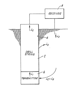
FIG. 1 is a schematic representation of a well bore
environment in which the present invention can be used.
FIG. 2 is a schematic circuit diagram of a prior art dc
clrcult .
FIG. 3 is a schematic circuit diagram of another prior
art dc circuit.
FIG. 4 is a schematic circuit diagram of a circuit com-
bining the circuits of FIGS. 2 and 3.
FIG. 5 is a block diagram of a bipolar signal apparatus
of the present invention.
FIG. 6 is a schematic circuit diagram of an implemen-
tation of the embodiment of the present invention shown in
FIG. 5.
FIGS. 7A-~B schematically depict different types of com-
mutated clamp implementations.
FIG. 9 is a schematic circuit diagram of a specific
implementation of the FIG. 5 embodiment.
FIG. 10 is a block diagram of one type of feedback cir-
cuit which can be used with the embodiment shown in FI~. 5.
FIG. 11 is a block diagram of another type of feedback
circuit which can be used with the embodiment of FIG. 5.
FIG. 12 is a schematic circuit diagram of a specific
implementation of the block diagram of FIG. 10.
Detailed Description of the Pre~erred Embodiments
In a particular aspect depicted in FIG. 1, the present
invention provides a well bore signal transmission system
:
_9_
comprising an electrically conductive drill string 2
disposed in a well bore 4 and further comprising a
transmitter 6 connected with an electrically insulating gap
to the drill striny 2 so that the transmitter 6 is disposed
in the well bore 4 with the drill string 2 but insulated
therefrom. The transmitter 6 transmits signals through the
drill string 2 to a receiver 8 which is not a part of the
present invention. In broader aspects of the present inven-
tion, the transmitter 6 can be used in other environments.
The transmitter 6 provides both amplification and a
bipolar output signal without using a transformer. One way
which the transmitter 6 could be implemented would be to
combine the prior art circuits shown in FIGS. 2 and 3 in a
manner illustrated in FIG. 4.
If the feedback voltage regulating circuits of FIGS. 2
and 3 are removed from the basic circuit, the output volta-
ges can be controlled in response to a gate d-rive signal
with a preferred duty cycle, namely, one which is propor-
tional to the desired output voltage. One method of
accomplishing this would be to replace the dc voltage
reference with an analog of the desired output voltage. If
the preferred duty cycle, in time sequence, is proportional
to the preferred output voltage, linear signal amplification
or generation results. Typically, the preferred output
voltage is that of a sine variation with respect to time.
The method of relating the duty cycle to the preferred out-
put signal may be that of pulse width modulation or any
--10--
suitable encoding method.
A fundamental restriction of either the positive or
negative voltage circuits of FIGS. 2 and 3, however, is that
they can generate an output voltage of only one polarity.
As mentioned, these two circuits can be combined as shown in
FIG. 4. Gate drive control signals G+ and G- operate tran-
sistors 10, 12 respectively, to conduct positive and nega-
tive current, respectively, in circuit with
inductor-capacitor integrators 14, 16, respectively.
Current from these integrators is alternately provided to
the load RL through output commutation transistors 18, 20 in
cooperation with diodes 22, 24, respectively.
If the gate drive control signals to the positive and
negative circuits of the FIG. 4 embodiment are alternately
driven in correspondence with the positive and negative por-
tions of the desired output signal and in proportion to the
instantaneous desired output voltage, bipolar operation can
be achieved. For a sine-wave output signal, the positive
and negative circuits would be used in alternate half
cycles, and their outputs would be commutated to the load in
alternate half cycles of the desired sine wave. It is pre-
ferred that the maximum gate on time be small with respect
to the output signal period and that the inductor-capacitor
integration time constant be large enough to provide accep-
table filtering of the voltage pulses and small enough to
allow an acceptable output signal rate-of-change. These are
easily satisfied if the pulse repetition frequency is two or
, .. ..
f~`J ~L~
more orders of magnitude greater than that of the desired
output signal; one order of magnitude greater is a minimum
acceptable ratio.
Although the circuit of FIG. 4 could be used in the EBT
environment illustrated in FIG. 1, the requirement for com-
mutation switching at the load is undesirable because the
signal at the load is characteristically of high current
(and low voltage) and the current related losses encountered
in the output commutating switches will reduce the maximum
achievable circuit efficiency.
FIG. 5 illustrates a preferred embodiment of the
transmitter 6 of the present invention. This combines the
desired features of the circuits of FIGS. 2 and 3 in a
manner that does not require commutation at the load. The
positive and negative gate outputs of the FIG. 5 circuit are
combined to provide an input to a shared integrator.
~ommutation is provided by alternating the gate control
signals to the positive and negative gate devices and by a
commutated clamp connected at the input of the integrator.
For the case of sine-wave amplification or generation,
appropriate signals having duty cycle versus time propor-
tional to each half cycle are alternately applied to the
gate control inputs during the appropriate half cycles of
the desired output sine-wave signal.
The feature of the circuit of FIG. 5 that permits this
combination is the commutated clamp that replaces the
separate diodes of the individual positive and negative uni-
:
`:
' .
--12-
polar circuits shown in FIGS. 2 and 3. If the diodes of
these two circuits were simply combined in parallel in the
circuit of FIG. 5, the input of the integrator would always
be connected to ground.
As shown in FIG. 5, positive gate 26 is connected to a
positive voltage supply and negative gate 28 is connected to
a negative voltage supply. Respective positive and negative
voltages from these supplies are connected to the input of
integrator 30 in response to duty cycle control 32 which is
responsive to input signal source 34 providing signal es.
Commutated clamp 36 is connected across integrator 30. If
the input signal source is an oscillator, the circuit of
FIG. S functions as a signal generator. If the input signal
source i5 an information containing signal, such as an
electrical signal representing pressure or temperature
measured in a well bore, then the remainder of the circuit
in FIG. S functions as a signal amplifier whose input is es
and whose output is eO. A preferred embodiment of the
amplification portion of the circuit shown in FIG. 5 is
shown in FIG. 6.
Batteries 38, 40 are connected to provide two different
polarity voltage sources. This is achieved in the FIG. 6
embodiment by connecting the negative terminal of the bat-
tery 38 to the positive terminal of the battery 40. The
positive terminal of the battery 38 is connected to the
collector of a bipolar transistor 42 implementing positive
gate 2~, and the negative terminal of the battery 40 is con-
-13- ~ ~ ~
nected to the collector of a bipolar transistor 44 imple-
menting negative gate 28. The bases of the transistors 42,
44 are connected to the duty cycle control means. The emit-
ters of the transistors 42, 44 are connected together at a
node 46. "Collector," "base" and "emitter" refer to the
respective terminals of bipolar transistors 42, 44 and they
also are intended to encompass corresponding terminals on
other types of transistors which could be used, such as
field effect transistors.
In the FIG. 6 embodiment, integrator 30 is implemented
by an inductor 48 and a capacitor 50. The inductor 48 has
one end connected to the node 46; and it has another end
connected at a node 52 to the capacitor 50, across which
load RL is to be connected. With reference to the environ-
ment shown in FIG. 1, the junction or node 52 of the induc-
tor 48 and the capacitor 50 is connected to a portion of the
transmitter which is in contact with the well bore and the
other end of the capacitor 50 is connected to the junction
of the batteries 38, ~0 and to the drill string 2. In an
alternate embodiment, the node 52 is connected to drill
string 2 while the junction of the capacitor 50 and the bat-
teries 38, 40 is connected to a portion of the transmitter
which is in contact with the well bore.
Commutated clamp 36 is connected across the inductor 48
and capacitor 50 for providing a current conductive circuit
in electrical parallel with the inductor and capacitor when
neither the transistor 42 nor the transistor 44 is con-
-14-
ducting through its collector and emitter terminals in
response to the duty cycle control means. Commutated clamp
36 will be more fully described hereinbelow.
The duty cycle control means in the preferred embodiment
as used in the environment illustrated in FIG. 1 receives an
input signal representing information to be transmitted to
the mouth of the well bore. In response to the input
signal, the duty cycle control means provides a control
signal. In the preferred embodiment, the duty cycle control
means includes conventional pulse width modulation means for
providing pulse width modulated actuating signals to the
bases of the transistors 42, 44. The signals provided to
the transistors 42, 44 turn them on (conductive) and off
(non-conductive) in response to the pulse width modulation
pulses occurring during the respective half cycles for a
sine wave. That is, during a positive half cycle, the tran-
sistor ~2 is turned on and off in accordance with the pulse
width modulation to communicate the positive voltage source
to the integrator containing the inductor 48 and the capaci-
tor 50. Likewise, during the negative half cycles, the
transistor 44 communicates the negative voltage source to
the inductor 48 and the capacitor 50. Thus, the two dif-
ferent polarity voltages and currents are periodically
alternately communicated through the respective gate
switches to the integrator.
Commutated clamp 36 provides means for delivering the
energy stored in the inductor field during gate-on intervals
'
;'..
-15~
to the load during gate-off intervals. This is accomplished
by clamping the inductor into a current conducting circuit
with the load (by clamping the inductor input to the common
electrical ground) during periods when neither gate is on.
This function, important for efficient circuit operation, is
well known in the switching power converter art. Since con-
ventional switching power converters are unipolar, the func-
tion described above can be provided by a diode connected to
block the voltage applied by the gate yet to conduct current
from ground to the load (and thus to deliver the energy
stored in the inductor field) during gate-off periods. In
the present invention, however, at particular times during
the process of amplifying bipolar signals, both positive and
negative source voltages will be gated to the inductor
input. Accordingly, a simple forward conducting, reverse
blocking device such as a diode cannot be used alone. Two
diodes, parallel connected in opposing polarity, cannot be
used alone because the gate voltage would always be shorted.
Also, in a specific preferred embodiment of the present
invention wherein a low voltage-high current output is
needed, the diode offset voltage would substantially reduce
the circuit's power efficiency. A low offset voltage, low
ohmic loss commutated clamp is preferred.
Representations of several embodiments for implementing
commutated clamp 36 are illustrated in FIGS. 7 and 8. In
each implementation the commutated clamp, in the interest of
efficiency, preferably is capable of holding the inductor
-16-
input very near ground potential while carrying relatively
high curxent. It is al90 preferable that it he capable of
switching from a clamped state to an unclamped state in a
time that is commensurate with the on-off switching time of
the gate switches. In operation, the clamps are on at all
times when the positive and negative gates are off, and off
when either gate is on. The switches and diodes illustrated
in FIGS. 7 and 8 represent the intended function only, and
may be implemented with any combination of appropriate devi-
ces readily known in the art.
FIGS. 7A and 7B illustrate two implementations which are
responsive to one and two control signals, respectively.
The control signals are on or off in periods of time related
to the gate on and off times. Thus, the commutation control
signals for closing the represented switches are the comple-
ment of the gate drive signals G~ and G- of FIG. 6.
FIGS. 8A and 8B illustrate a type of clamp which is uni-
directionally conductive during the operative half-cycle of
each respective gate switch. That is, the left diode as
viewed in FIGS. 8A and 8B will be connected into the circuit
and the right diode disconnected from the circuit when the
positive gate is used. The left diode will be disconnected
and the right diode connected when the negative gate is
used.
The circuits of FIGS. 8A and 8B can also be used in a
self commutating manner. Such operation could be achieved
by a sensing means at the inductor input (node 46) causing
.,
r~
--17--
the clamp to switch from on to of when either gate is
driving the inductor.
FI~. 9 is a schematic circuit diagram of a specific cir-
cuit employing the commutated clamp type of FIG. 7A. The
particular implementation of FIG. 9 is a low current proto-
type form, but test results indicate that a high current
version of this circuit should be well suited to EBT signal
amplification or generation. Like parts between FIGS. 5, 6
and FIG. 9 are indicated by the use of like reference
numerals.
The basic apparatus illustrated in FIG. 5 does not show
a feedback loop; however, the output eO can be controlled to
provide constant voltage, constant current or constant power
by using a suitable known type of feedback loop. These
include the use of a variable gain amplifier 54 (FIG. 10)
having the input signal eS as one input. The other input is
received from the feedback loop.
The feedback loop shown in FIG. 10 provides a means for
obtaining a preferred output signal voltage that is
invariant with output load resistance. In operation, an
appropriate signal, denoted Y, is obtained from the
amplifier signal output. Signal Y is proportional to the
instantaneous signal output voltage. Because the output
siqnal is bipolar and a unipolar control siqnal is required,
the signal Y is first rectified as indicated by block 56 in
FIG. 10. The rectified signal is then offset by an
appropriate reference signal VR (block 58) to represent a
-18~ &~5
relative measure of the output ac signal as a quasi-dc error
signal. The quasi-dc error signal is then integrated and
amplified (block 60). In practice, the integration time
constant is preferably at least several times greater than
the period of the bipolar output signal. Finally, the pro-
cessed quasi-dc error signal is applied to the control
input, denoted X in FIG. 10, of the variable gain amplifier
5~. The combined result of the operation of the described
functions is to stabilize the output signal voltage relative
to a predetermined amplitude established by VR. In effect,
the amplifier source resistance is reduced to zero so that
output load resistance variation does not result in an out-
put voltage variation.
In a second application of feedback control, the same
function obtains except the output eO is controlled to pro-
vide an output ac current that is independent of output load
resistance. The only difference in implementation is that
the signal Y is proportional to the output ac current rather
than to the ac voltage. Any conventional current sensing
means can provide the required signal. Also, in the opera-
tion of the bipolar amplifier, a signal that is proportional
to the amplifier output current can be obtained by
appropriate sensing in any one or more of the gate or com-
mutated clamp elements. Subsequent processing is equivalent
to that of the constant voltage feedback application except
that a constant amplifier output ac current proportional to
the reference VR is provided. FIG. 12 is a schematic cir~
,
'
f~.
cuit diagram of a specific implementation of a constant
current feedback loop wherein variable gain amplifier 54
consists of a conventional multiplier circuit. In the
illustrated configuration, the multiplier output is equal to
es(X+5)/lO. As error signal X may vary from -5V to +5V,
output signal es' may vary from O to es such that a constant
ac output current in-dependent of load resistance may
obtain.
The third type of feedback loop, one by which a constant
power output is obtained, is illustrated in FIG. 11. This
provides an output power level that is independent of output
load resistance. Signals Y and Y' representative of the
amplifier's output voltage and current are processed as
described in the previous types of feedback loops to provide
both voltage and current related quasi-dc signals (blocks
62, 64). Subsequently a single quasi-dc signal proportional
to the product of these two signals is obtained by conven-
tional signal multiplier processing (block 66). The
resultant signal, which is proportional to the output signal
power, is finally processed relative to the reference VR
(block 68) and applied to the variable gain amplifier at
input X. This achieves a constant amplifier output ac power
proportional to the reference VR.
The circuits and functions described hereinabove can be
readily implemented with many types of conventional circuit
devices, such as bipolar transistors, field effect tran-
sistors, diodes and other common circuit components. Also,
: ;
-20-
a plurality of devices can be connected in parallel, for
instance in the gate switches or commutated clamp, so that
high current flow can be shared among the devices.
Although the operation o~ the present invention has been
generally described hereinabove, the operation with respect
to transmitting a very low frequency signal on the drill
string 2 disposed in the well bore 4 will be specifically
described. Within the well bore 4 there will be generated a
very low frequency signal by some other device, which signal
contains information to be transmitted to the surface. For
example, a downhole pressure sensor output may be used to
encode a very low frequency oscillator signal so as to con-
vey pressure data. This signal will need to be amplified
for transmission up the drill string 2 to the receiver 8.
Using the present invention, a respective first pulse width
modulated control signal is generated in response to each
positive half cycle o~ the encoded very low frequency
signal. A respective second pulse width modulated control
signal is generated in response to each negative half cycle
of the encoded very low frequency signal. This is
accomplished through the duty cycle control means 32 in a
known manner. These signals are series of pulses whose
widths are related to the amplitude of the encoded very low
frequency input signal.
In response to the first pulse width modulated control
signal, a positive voltage/current will be applied/conducted
to an input of the integrator 30. This is generally not
-21-
continuous because the pulse width modulated control signal
will have alternate on and off periods within the respective
positive half cycle. Similarly, during each negative half
cycle of the encoded very low frequency signal, a negative
voltage/current is applied/ conducted to the input of the
integrator 30 in response to the second pulse width modu-
lated control signal. With respect to the embodiment
illustrated in FIG. 6, the voltages/currents are
applied/conducted by actuating the respective transistors
42, 44 implementing gate switches 26, 28, with the first
pulse width modulated control signal and the second pulse
width modulated control signal, respectively. That is, G~
is implemented by the aforementioned first pulse width modu-
lated control signal and G is implemented by the aforemen-
tioned second pulse width modulated control signal.
At the integrator 30 of the transmitter, a very low fre-
quency current is provided to the drill string 2, which is
connected to the output (node 52 in FIG. 6) of the integra-
tor 30, in response to the positive and negative inputs to
the integrator 30. This includes switchably connecting the
integrator 30 directly into a current loop with the drill
string 2 when neither the first pulse width modulated
control signal nor the second pulse width modulated control
signal causes the positive or negative voltage/current to be
applied/conducted to the input of the integrator 30. For
the preferred embodiments, this switchably connecting step
includes switchably connecting the input (node 46 in FIG. 6)
-22- 2~
of the integrator 30 to electrical ground such as is
illustrated in the particular implementation of FIG. 9 and
more generally in FIG. 5. More generally, the input of the
integrator is connected into a current conductive circuit
with the load.
Thus, the present invention is well adapted to carry out
the objects and attain the ends and advantages mentioned
above as well as those inherent therein. While preferred
embodiments of the invention have been described for the
purpose of this disclosure, changes in the construction and
arrangement of parts and the performance of steps can be
made by those skilled in the art, which changes are encom-
passed within the spirit of this invention as defined by the
appended claims.
'