Note: Descriptions are shown in the official language in which they were submitted.
9S~
This invention relates to a connector apparatus for
IC Packages, more particularly, to a connector apparatus
for receiving and ejecting a memory card which is con-
nected to CPU, DMA, or the like, in a electronic
device for reading out data stored in the Package to
perform predetermined tasks.
In an electronic device, such as a microcomputer,
it has been common practice to mount an IC package, such
as a memory card, in an electronic device body, if
necessary, in an electrically connected fashion so as to
accomplish, for example, an extended application. For
this purpose, a connector apparatus has been used in the
art.
The conventional connector apparatus for an IC
package is of such a type that it has a substantially
U-shaped frame with a pair of guide grooves provided on
its inner side frame portions and a connector section
provided as a connection frame portion between the side
frame portlons and, in use, a plate-like IC package is
inserted via an access hole into the device space, while
being guided along the guide grooves, and held there
with its widewise array of socket termlnals electrically
connected to an associated pin terminal array of the
connector section.
In the connec-tor apparatus as set out above, an
eject mechanism is provided which, when the package is
not in use, electrically disconnects the package from
~, .
.
.
.
: ', ' ' '. '
. ' ' :
- 2 - ~ ~ S ~
the device body. The eject mechanism is so operated
that it is rotated around its fulcrum to cause an
engaging hook means which is provided on the forward end
of the plate-like member to engage with the forward.end
edge of the package whereby it is possible to eject the
package out of a storage site.
In a recent trend toward accomplishing a thin,
lightweight compact electronic device, there has also
been unending demand for a corresponding compact device
per set which receives IC package into its storage space
and holds it electrically connected with the electronic
device.
In this type of connector apparatus for IC package,
in order to prevent a deformation at the engaging hook
means of the forward end of the lever member due to a
load involved there, the lever rnember has to be
thickened and, further, a strong structure needs to be
achieved at the fulcrum site, failing to obtain a
compact device. It is thus not possible to make the
: 20 device thinner in the direction of the thickness of the
package.
It is accordingly the object of the present
invention to provide a connector apparatus for IC
package, which can be obtained as a thin, lightweight
~5 compact unit, whlle being made closely equal to the
dimension of the package per se and can also be
: obtained as a very durable unit in spite of its thin
.
.
. ~ :
- 3 -
structure.
In order to achieve the object of the present
invention, there is provided a connector apparatus for
IC package; comprising: .
a housing plate member having cutouts formed in
predetermined positions;
a pair of guide frame members arranged at an
interval substantially equal to a width of a plate-like
IC package and to be parallel to each other on both
sides of the housing plate member;
a connector section provided at one end of the
guide frame member and having connecting pins to be
electrically connected to the package;
a pull-out plate member slidable over a surface of
the housing plate member and having engaging hooks
to engage with a forward end face of the package
electrically connected to the connector section via the
cutouts of the housing plate member, and
an ejection arm/lever rotatably ~ournaled over the
surface of the housing plate member and coupled at one
end to the pull-out plate.
According to the present invention, when the
e;ection lever is rotated with a journaling structure as
a center, the lever coupled at one end to the pull-out
plate is slidably moved over the surface of the housing
plate member. When this occurs, the package is ejected
through the engagement of the engaging hooks with the
- 4 - ~ ~ S ~
front end face of the IC package to cause the IC package
to be electrically disconnected from the connector sec
tion.
This invention can be more fully understood frpm
the following detailed description when taken in con-
junction with the accompanying drawings, in which:
Fig. 1 is a plan view showing one embodiment of the
present invention;
Fig. 2 is a bottom view showing the embodiment of
the present invention;
Fig. 3 is a cross sectional view showing a shaft
support section of an ejection lever in the embodiment
of the present invention; and
Fig. 4 is a side view showing the embodiment of the
present invention.
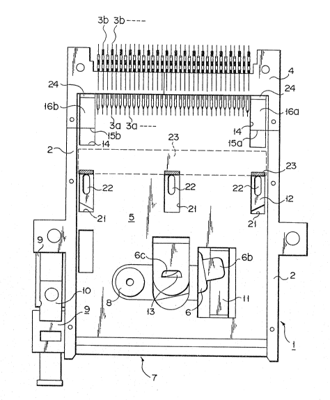
Fig. 1 is a plan view showing a connector apparatus
according to one embodiment of the present invention,
the arrangement shown in this Figure normally
corresponding to a ~circuit boardl~ side in an electronic
device for reading data stored in the package.
The connector apparatus 1 comprises a pair of guide
frame members 2, 2 made of a nylon, defining an interval
somewhat greater than the width of IC package (memory
card)~ not shown, and having a length substantially
equal to the depth of the package and a thickness
substantially equal to the thickness of the package, a
connector section 4 having connecting pins 3a fitted
_ 5 _ .~5~
into socket terminals provided on the package side and
connecting pins 3b connected to those provided on the
side of the device, and a housing plate member 5 made of
a metal, fixing the guide frame member 2, 2 in place,
having a later-described e;ection mechanism formed on
its surface, and, upon being mounted in place in the
electronic device, defining a storage space of the
package relative to a circuit board on the side of the
device through the guide frame members 2.
Fig. 2 is a bottom view of the connector apparatus
1 as seen from the rear side as distinct from the side
shown in Fig. 1, the ejection mechanism being prin-
cipally shown in Fig. 2.
An ejection lever or arm 6 is made of a metal and
supported by a rotating axis 8 on the lower surface side
of the housing plate 5 at an area near an access hole 7
leading to the package storage space. In order to
rotate the ejection }ever 6 around the rotating axis 8,
one end 6a of the ejection lever 6 is rotatably coupled
by a rotation shaft lla to one end of a slide member 10
which is slidably moved in a one-piece molded guide 9.
A tongue 6b is provided integral with the other end of
the ejection lever 6. The tongue 6b is, for example,
strucked out of the housing plate 5 and located ln a
manner to be placed in slidable contact with the inside
surface of the band-like slide guide 11 somewhat raised
from the housing plate surface. Thus, the ejection
- 6 - ~ 3~
lever 6 is so constructed as to be rotatable in a plane
parallel to the housing plate 5. The ejection lever 6
has a raised section 6c projected toward the housing
plate 5 side.
Reference numeral 12 shows a pull-out metal plate
which can withdraw the package (not shown) out of
electrical connection with the connector section 4 of
the connector device 1 when the package is not in use.
The pull-out plate 12 has an engaging claw 13, as a
raised claw, at its end and engages with the raised
section 6c formed on the driven side as distinct from
the rotating axis (drive side) 8 for the lever 6. The
pull-out metal plate is of such a type that it is sli-
dable in a pull-out direction of the package over the
housing plate 5 upon rotation of the ejection lever 6.
The pull-out metal plate 12 has extending arms 16a and
16b one at each opposite side. The pull-out metal plate
further has bent sections 15a, 15b in a stepped relation
such that their forward ends are upwardly projected via
cutouts 14, 14 provided at corresponding area of the
housing pla-te member. Thus the package stored in the
storage space of the connector device 1 has its surface
placed in direct contact with the arms 16a and 16b of
the pull-ou-t plate 12. The forward ends of the arms 16a
and 16b are bent to provide engaging hooks 24, 24
engaging with a socket-side end face, that is, the
forward end face, of the IC package.
- 7 - ~ q~
The package needs to be electrically shielded and,
in orc]er to achieve this, three projections 22 are pro-
vided at corresponding places, by an extrusion molding
method, in the middle portion of -the pull-out metal
plate (conductive plate) such that the~ are projected
toward the storage space side via through holes 21 pro-
vided at the corresponding areas of the housing plate 5
to allow them to contact with the outer surface of the
IC package inserted.
Fig. 3 is a cross-sectional view showing the shaft
support section of the ejection lever 6. Since the
rotation shafts 8 and lla are of the same type, only one
shaft 8 will be explained below in conjunction with
Fig. 3 and explanation of the shaft lla is, therefore,
omitted.
That is, a tubular projection 6d is provided as one
portion of the ejection lever 6 and made of, for
example, a stainless steel. The tubular projection 6d
is fit~ed in the bearing hole 18 provided in the housiny
2~ plate 5 made of, for example, a stainless steel. The
rotation shaft 8 made of a brass has a flange 8a at one
side and is fitted in a center through hole provided in
the tubular projection. The other side of the rotating
axis is caulked to prevent the rotating axis from being
slipped off the center through hole. The rotating axis
is rotatable in the bearing hole 18 in accordance with
the movement of the lever 6. In the arrangement shown
- 8 -
in Fig. 3, the ejection lever 6 is repeatedly rotatable
while the outer surface of the tubular projection 6d of
the ejection lever 6 contacts with the inner wall
surface of the bearing hole 18 of the housing plate 5.
Since the housing plate 5 is made of the same material
as that of the ejection level, it is possible to achieve
a high wear resistance and hence to achieve a remarkably
enhanced endurance at the bearing area.
The problem with the endurance of the bearing area
has conventionally arised from, for example, a clearance
between the rotation shaft and the insertion hole of the
ejection lever due to, for example, the wear of the
axis and a resultant reduction in an IC package pullout
stroke length. That ls, a reliability problem has been
involved upon wlthdrawal of the package.
It has been found that the aforementioned bearing
structure of the ejection lever of the connector appara-
tus according to the embodiment of the present invention
can fully withstand about 20,000 ejection operations, a
flgure which is generally required in this field of art.
Further, the connector apparatus of the present
embodiment is of such a type that a connector section 4
can be separated from an ejection mechanism-equipped
housing plate 5 side by a simpler operation. Fig. 4 is
2s a side view showing the connector apparatus. In Fig 4,
an engaging arm, not shown, is provided integral with
each side section of the connector 4 made of elastic
.
,
,, '
- 9 ~
material and an engaging pro~ection 19 is provided on
the forward end of the engaging arm. The engaging arm
of the connector section 4 is inserted into a receiving
section provided by both the bent side portion o* the
housing plate 5 and partial recess formed at the side
surface of the guide frame member 2. The engaging
projection 19 is fitted into the engaging hole 20 -
provided in the bent side surface of the housing
plate 5.
The connector section can be freely and readily
attached to, or detached from, the side of a connector
apparatus by bringing the engaging projection 19 of the
engaging arm of the connector section into and out of
~ engagement with the engaging hole 20 provided on the
guide frame~member 2 side and hence the housing plate 5
side.
The guide frame member 2 is secured by screws to
the housing plate 5.
Whe~ the package is mounted in the electric device
according to the present invention, it is inserted into
the sto~rage space vla the access 7 of the connector
device~l to fit the socket terminals of the package over
the pin terminals of the connector section 4. At this
time, the forward end face of the package engages with
the engaging hooks 24, 24 of the pull-out metal plate 12
:
to move the metal plate 12 in a forward direction. ~s a
result, the ejection lever 6 is rotated around the
- 1o ~ 6,,',
rotating axis 8, causing the slider member 10 to be
projected.
With the package held in the storage space, the IC
package is grounded through the pull-out plate 12 whose
projections 22 are connected via the through holes 21
of the housing plate 5 to the package surface and then
through the ejection lever 6, housing plate 5 and
screws 25.
By so doing, it is only necessary that only one
surface of the package, that is, only its surface facing
the housing plate 5, make electrical contact with the
projections 2Z of the pull-out plate 12. Therefore, no
particular consideration needs to be paid to the other
surface of the package whi.ch faces the circuit board in
the device~ It is thus possible to provide a desired
printQd circuit pattern, for example, on that surface.
Further, since there is no intervening object
between the circuit board of the device and the one
surface of the package, electric contact can be made
between the side of the package and the circuit board
and this can be so done at any proper position with the
use of a thin metal plate of, for example, a predeter-
mined electric conductivity. It is possible to properly
print a desired circuit pattern on each side of the
package.
When the package is withdrawn out of the storage
space, the slider member 10 is pushed, causing the
e;ection lever 6 to be rotated around the rotating
axis 8. This rotation causes the pull-out plate 12 to
be moved over the surface of the housing plate 12 along
the guide frame members 22 with the raised section 6c
hooked by the engaging claw 13, so that the package is
withdrawn out of the storage space through the utiliza-
tion of the engaging hooks 24, 24 on the forward end of
the arms 16a, 16b.
In the aforementioned connector device 1, the
pull-out plate 12 is freely moved over the surface of
the housing plate 5 and, if a debarring process which
has to be done, for example, at the edge of the punched
through hole 21 of the housing plate 5 is omitted so as
to lower the manufacturing cost, then there is a possi-
billty that the contacting surface of the draw-out plate
12 will be scraped off by the burr. It is preferable
that, in order to prevent the occurrence of electrical
faults resulting from the drop of the metal scrapings
onto the package or connector section, a plate-like
covering 23 made of, for e~ample, polyethylene be joined
to that area of the draw-out plate 12 where the draw-out
plate 12 is moved over the through holes of the housing
plate 5.
The connector apparatus according to the present
embodiment has a dimension, that is, a thic~ness about
1.4 times that (about 3 mm) of the package, a width
corresponding to a total of the width of the package
- 12 -
plus that of the guide frame member 2, and a depth
greater than the depth of both the depth of the package
and thickness of the engaging hook 24 involved upon
engagement of the engaging hooks 24 with the socket-side
end face of the package. It is thus possible to obtain
a thin compact unit.
As will be evident from the above, the connector
apparatus of the present invention can be achieved with
much less number of component parts than a conventional
connector apparatus for IC package of the same type. It
is thus possible to make the whole outer dimension of
the CGnnectOr apparatus closely equal to that of the
package per se and hence to provide a thin, durable
compact connector apparatus.