Note: Descriptions are shown in the official language in which they were submitted.
`- 2050658
DUAL HARDWARE CHANNELS AND HARDWARE CONTEXT
SVVITCHING ~ A GRAPHICS RENDERING PROCESSOR
BACKGROUND
The field of the invention is display systems and in particular graphics
s processors for display systems that provide multiple channels and context
switching belwæn çh~nnFl~.
Many types of graphics systems require fast response to opel~tor inputs
and cursor movements. Often, a fast response must occur while a graphics
processor is
.
2050658
e
performing a low priority task, such as generating a background map. Existing graph-
ics processors are implemented with a single channel that cannot respond rapidly to pri-
ority tasks. Such systems have relatively poor response to higher priority tasks. This
is because the graphics processor is implemented to finish the current task before in-
5 voking a next task. There is no provision for assigning priorities to tasks. This is be-
cause, even if a subsequent task is a higher priority task, the graphics processor must
complete the current task before invoking the higher priority task.
SUMMARY OF THE INVENTION
A prioritized multiple channel configuration having context switching solves
important graphic system problem of fast response. The present invention is an im-
provement in graphics processors, using multiple channels having context switching
and FlFOs to provide rapid response to higher priority tasks. A graphics processor
servicing a first channel task is interrupted when a higher priority task is available in a
15 second channel. Context switching facilitates interrupting of the lower priority first
channel task, then saving of the context of the first channel task, then pelro~ ing
higher priority second channel task, then restoring the interrupted first channel task,
and then continuing with the processing of the restored first channel task.
The present invention efflcienlly solves the problem by providing two priori-
20 tized input channels sharing a single graphics processor. The graphics tasks requiring
fast update are usually sent through the high priority channel. The graphics tasks not
requiring fast update are usually sent through the low priority channel. Also, multiple
host processors are readily accommodated and can each use both channels.
- A preferred embodiment of the present invention comprises one or a plurality of
25 stored program computers for generating a plurality of display lists. Each display list
includes a plurllity of graphic instrllc~ions. A plurality of FIFOs are coupled to the one
or more stored program computers for storing the plurality of display lists. A graphics
processor is coupled to the plurality of FilFOs for generating graphic pixel signals in re-
sponse to the plurality of display lists stored by the plurality of FlFOs. A bit map
3() memory is coupled to the graphics processor for storing the graphic pixel signals. A
display monitor is coupled to the bit map memory for generating a display in response
to the graphic pixel signals stored by the bit map memory. The plurality of FlFOs may
each store a different display list.
The graphics processor the present invention includes a context switching cir-
35 cuit for switching context between different display lists stored by different ones of the
plurality of FJFOs and for generating the graphic pixel signals in response to the differ-
ent display lists. It also includes an inlerrupt input circuit for generating an intermpt
20506~8
signal and an interrupt execution circuit coupled to the interrupt input circuit and to the
plurality of FlFOs for interrupting the generation of graphic pixel signals in response to
the interrupt signal and in response to a first display list stored by the plurality of
FIFOs.
S The in~e-- upt input circuit generates graphic pixel signals in response to the in-
terrupt signal and in response to a second display list stored by the pluraiity of FIFOs.
Tt includes a restore control circuit coupled to the interrupt execution circuit for generat-
ing a restore signal in response to the second display list stored by the pluralily of
FlFOs and includes a restore execution circuit coupled to the restore control circuit and
I () to the intermpt execution circuit for restoring the context of the first display list in re-
sponse to the restore signal. It also includes a concurrent processing circuit coupled to
the plurality of FlFOs for processing at least one of the plurality of display lists concur-
rently with the generating of the display list generated by the stored program computer.
It also includes a nested subroutine circuit for controlling the generating of the graphic
pixel signals under nested subroutine control.
In addition, a method of providing context switching in a display system com-
prising a F~FO and a graphics processor is disclosed. The method comprises the fol-
lowing steps. Transferring a first display list to the FIFO. Initiating processing of the
first display list by the graphics processor. Transferring a second display list to the
FIFO. Interrupting processing of the first display list by the graphics processor and
storing a context of the first display list. Initiating processing of the second display list
by the graphics processor. Detecting completion of processing of the second display
list by the graphics processor. Restoring the context of the first display list. Contin-
uing processing of the first display list by the graphics processor.
Accordingly, a feature of the present invention is to provide an improved dis-
play system and method. Another feature of the present invention is to provide an im-
proved graphics processor. Another feature of the present invention is to provide a
general purpose graphics processor. Another feature of the present invention is to pro-
vide multi-level nested inlel- IJpt capability for a graphics processor. Anolher feature of
the present invention is to provide a nested subrolltine capability for a graphics proces-
sor. Another feature of the present invention is to improve response time of a graphics
processor. Another feature of the present invention is to reduce latency time of a graph-
ics processor. Another feature of the present invention is to provide concurrent down-
loading and graphics proces~ing. Another feature of the present invention is to provide
DMA downloading of display lists. Another feature of the present invention is to pro-
vide a multiple channel graphics processor. Another feature of the present invention is
to provide a multiple channel FIFO input for a graphics processor. Another feature of
`~ 4 20506~i8
the present invention is a context switching interrupt strueture to f~l ilitate higher
priority proeescin~.
s
Other aspects of this invention are as follows:
A display system characterized by:
a stored p.o~ ... computer for generating a plurality of display lists, each
display list including a plurality of graphie instructions;
a plurality of FlFOs coupled to the stored program computer for storing the
plurality of display lists; and
a graphies p~cessor coupled to the plurality of FlFOs for generating graphic
pixel signals in response to lhe plur~lity of display lisls stored by ~he pluralily of
Fl FOs.
In a display system comprising: a stored p~o~la~l eo.,.~ ter for generating
display lists, a display memory eoupled to the stored 1~~'~"l co.n~,ute~ for storing the
display lists, a graphies p.ocessor eoupled to the display memory for generating pixel
signals in le~onsG to the display lists, a eontext switehing arrang~metlt that inîc.r~ces
between the storcd ~lO~ll CO~"P~ and the graphics ~.ocessor, said eontext
2 o switehing arrangement is eha a~t~,fized by:
first and seeond hardware eh~nnelc eomprising high and low priority
p.~ssing ch~nn~lc;
a dual ehannel F~FO eontroller eoupled to the first and seeond hardware
channels for interfaeing between the stored program C4~P~ and the display memoryand seleetively loading the display lists into first and second ~l~O buffers in the display
2 5 memory;
an inl~,, l upt eircuit eouple d to the graphies p,~)eessor and the display memory
for inîc,.lupling the p,ocessing of a low priority display list and initi~ting the proeessing
of a higher priority display list; and
a plurality of eontext l~l;ist~ for storing eontext attributes ~ccoc1~t~d with each
of the display lists and a ~ lb~cL- multiplexer for restoring the attributes of the low
3 o priority display list onee the higher priority display list has been p,oces~d
A~
4a
205065~
~n a display system comprising a FrFO and a graphics processor, a method
is characterized by the steps of:
transferring a first display list to the FlFO;
initiating processing of the first display list by the graphics processo-,
transferring a second display list to the FIFO;
inle.l~pling pr~ce~sing of the first display list by the graphics processor and
storing a context of the first display list;
initiating processing of the second display list by the graphics processor,
detecting co.. pletion of processing of the second display list by thc graphics
processor,
restoring the context of the first display list; and
continuing processing of the first display list by the graphics processor.
~n a display system comprising: a stored pro~;lalll computer for generating
display lists, each display list including a plurality of instructions, a plurality of ~l~OS
coupled to the stored program computer for storing the display lists, a graphicsplocessor coupled to the plurality of FlFOs for generating pixel signals in response to a
display list, an intellupt circuit coupled to the ~,laphics plvcessu~ for int~.lul)ling
operation thereof, and a context memory couple~l to the graphics pç~cessol and to the
interrupt circuit for storing a context in l~,l.once to int~,.lu~ltion of operation, a method
2 o is characterized by the steps of:
transferring a first display list from the stored p~gla-n computer to a first one
of the plurality of thc FlFOs;
inidating processing of the first display list by the graphics p,ocesso-,
L ansf;,.l;ng a second display list from the stored ~loE,Ialn conlputel to a second
one of the plurality of the F~FOs;
2 5 inte~l Upling ~I-xessing of the first display list by thc graphics processor and
storing a context of the-first display list in the context memory;
initiating plvccssing of the second display list by the graphics ploCe,SSOI,
detecting completion of plvcessing of the second display list by the graphics
pl~cesso.,
restoring the context of the first display list stored by the context memory; and
3 co.";n-.ing p-ocessing of the first display list by the graphics proccssor.
I ? ~
-
2050658
'
4b
BRIEF DESCRIrTION OF TI~E DRAWINGS
The various features and advantages of the present invention will become ap-
parent from the following detailed description taken in conjunction with the accompany-
ing drawings, wherein like references numerals designate like structural elements, and
in which:
Fig. I is a block diagram representation of a graphics processor system that
employs dual hardware channels and hardware context switching in accordance withthe principles of the present invention;
Fig. 2 is a detailed block diagram of the graphics processor of Fig. l;
Fig. 3 is a block diagram representation of the interface between the graphics
processor and a bus that illustrates aspects of the present invention;
Fig. 4 is a detailed block diagram of the context register shown in Fig. 2;
Fig. 5 is a detailed block diagram of the dual channel FIFO controller of Figs. 2
and 3;
Fig. 6 is a memory map ~ csentation of a PJFO; and
Fig. 7 is a memory map representation of an attribute stack.
2()
DETAILED DESCRIPTION
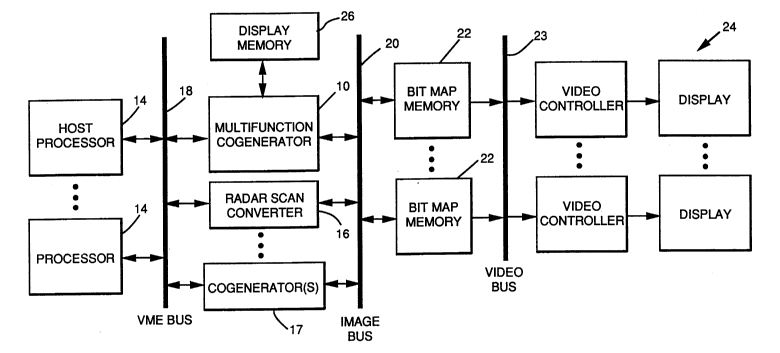
Referring to the drawings, FIG. 1 is a block diagram of a generalized graphic
display system including a dual channel multifunction cogenerator 10 of which the pre-
sent invention forms a part. FIG. 2 sh-)ws a block diagram of the cogenerator 1() of
which a dual channel FIFO controller 38, 40 and context registers 42 of the present in-
vention forms a function~lly distinct part. The cogenerator 10 is a dual channel, hard-
ware based device which operates in conjunction wilh one or more general purpose data
prc!cessing systems, such as a military command and control system, wherein the sim-
plified system is shown in FIG. 1. Brietly, the system comprises one or more real time
3() data processors 14 and other real time data accumulating devices such as a radar system
16 and other cogenerators 17. The host processor 14 and the radar scan converter 16,
for example, feed data into the cogenerator 10 via a multifunction bus 18 where it is
combined with graphics data generated by the cogenerator 10. The cogenerator 10 out-
puts a complete set of data for generation of a graphics display via a 64-bit bidirectional
interconnect image bus 20 into a bit map memory 22 and then by way of a video bus 23
to a display system 24. The cogenerator 10 m~ly include various other input devices
205Q65~
s
such as manual input output devices, multiple real time processors, bulk memory de-
vices and the like.
A det~ile4 des.;li~lion of the cogener~tor 10 is given in commonly ~ n~d
- 5 United States Patent No. 5,276,798 entitled,"Multifunction Cogenerator". In over-
view, however, the cogenerator 10 is a high performance single chip graphics render-
ing pl~cessor. It g~"~clates m~ iple graphics primitives and performs general purpose
p,-~ce ~ g functions. The cogenerator accepts graphic commands over a thirty-two bit
bidirectional host input port from a processor such as the host processor 14 of FIG. 1.
10 The cogenerator 10 p,ocesses these commands and then draws into the bit mapped
memory 22. The cGge.lc~ator 10 "draws" into the bit ll-apped memory 22 over the im-
age bus 20. "Drawing" is pe.rol-"ed by entering binary one and zero signals (drawing
ones and drawing zeros herein) into individual memory locadons of the bit mappedmemory 22. Typically, the bit mapped memory 22 has multiple memory layers with
15 the layers corresponding to color and intensity of graphic display pixels. The image
bus 20 is a 64 bit bidirectional multi-user bus. The cogenerator 10 can draw graphic
primitives such as symbols, polylines, rectangles, circles, ellipses, arcs, polygon fills,
and perfo~n bit block transfers (BITBLT) between the cogenerator 10, the host proces-
sor 14, and the bit mapl)cd memory 22.
Directly associated with the cogenerator 10 is a tri-ported display memory 26.
The display memory 26 stores all commands and parameters and includes ap~,lopliate
logic required for the cogenerator 10 to function properly. The memory address space
in a working embodiment is 4 megabytes by 32 bits. The cogenerator 10 interfaceswith either DRAMS, SRAMS, and/or PROMS. The display memory 26 is accessible
25 by the cogenerator 10 display list processor 28, the cogenerator 10 internal graphics
generator 30, and the host processor 14. Stored in the display memory 26 are two first
in, first out (FIFO) memory buffers one of the buffers being assigned a higher opera-
tional priority than the other and there being one buffer memory for each of two draw-
ing channels. An address stack is provided for each FI~O buffer to store subroutines
30 calls. An attribute stack stores all internal cogen~.~tor attributes for hardware context
switching, a sin/cosine table for drawing graphics, and up to 128 font tables to draw
stroked and/or dot matrix symbols and characters. A large display list region is also
provided.
The display memory 26 is comprised of up to four million words of RAM or-
35 ganized as 32 bit data words and appropriate buffer logic. The contents of the display
memory 26 may be organized as shown in Table l below. The host processor 14 has
the ability to pe.ro~ random reads and writes at any address within the display mem-
~,.,
.:
20506~
h
ory 26 address space. The cogenerator I () monitors tl1e input of data from the host pro-
cessor 14 to tl)e display memory 26 to synchronize updating of data from the host pro-
cessor 14 with the output of grapl1ics signals Iherefrom.
A dual channel FlFO buffer conlroller 38, 4() interfaces the cogenerator 10 to
S the host processor 14. Tlle FIFO buff~r controller 38, 4() are responsible for perform-
ing all interfacing duties such as proper "lland sllaking" when the bus 18 is performing
data transfers. The host processor 14 is able to both read and write to the cogenerator
10 and the display memory 26. Whell the host processor 14 reads or writes to the dis-
play memory 26, the FIFO buffer controller 38, 4() actually perform the read or write
1() operations to the display memory 2~ for the host processor 14. An address stack is
provided internally within each FIFO buffer controller 38, 40 to store subroutine calls,
an attributes stack to store all internal .ll~ributes re(luired by the cogenerator 10 to per-
fonn hardware context switching, a sine/cosine table of drawing conics and primitives,
up to 128 font tables to draw both stroked and dot matrix symbols and characters and a
large display list region. The FIFO buffer controller 38, 40 is also responsible for arbi-
trating high and low priority channels to the cogenerator 10.
A display memory interface unit 35 performs the actual display memory 26
memory cycles. It is essentially a tri-port memory controller. The display memory 26
is used by both the host processor 14, and the cogenerator 10.
A display list plucessor 28 performs all of the cogenerator 10 command and
display list processing. Commands are sent to the cogenerator 10 from the host pro-
cessor 14. The display list processor 28 handles the various ways that commands can
be sent to the cogenerator 10. The display list processor 28 interfaces to the display
memory 26 using the display memory interface unit 35, reads commands from tlle
~Iro buffers as well as perfonms olher lunclions. Whell a coml11alld is given to tlle
- display list processor 28, the display list processor 2X processes the command and de-
em~ines what action to take. The cogel1erator 1() provides many differ~l1t con1m.lnds
~nd se-3uellces.
3()
Context registers 42 store all of the cogeneralor attributes. These attributes de-
fine the current state of the cogenerator l(). The current slate may include a large num-
ber of paramelers SUCII as: cogeneralor operatiol1al mode; draw pointer posilion; fore-
ground color; background color, clipping window dil11ensions; etc. l`he conlents of the
cogeneralor 1() are important as they derlne the l-ersoll~lity of the cogenerator l() at any
''''~'A
- 205065~
given time and all attributes are user programmable. Tllis gives a user consi(lerable
flexibility in operating the display system.
Also provided is a readback multiplexer 44 which is a large data multiplexer. Itis used to multiplex data to the display memory interface unit 35 which is directed to
S either the display memory 26 or back to the host processor 14 via~bus 18. Three
sources of re~dbark data are the context registers 42, a graphics generator 34 defined
within the dashed block in FTG. 2, and the block texturing and complex clipping pro-
cessor 30. If the data is intended for the host processor 14 it will be sent through the
FIFO buffer controller 38,40 by the display memory interface unit 35. The graphics
10 gene. alol 34 is connected to the readback multiplexer 44 for various co~n-,. alOI 10
drawing operations. The block texturing and complex clipping processor 30 also sends
data to lhe readback multiplexer 44 for various cogenerator 10 operations.
The graphics generator 34 generates all of the cogenerator 10 primitives and
symbols and pc,rol,l.s bit block transfers (BITBLTs). The graphics generator 34 in-
15 cludes a multiprocess scheduler 46, a command generator 41, an area fill conic andvector generator 43, a symbol generator 45, and a BITBLT address generator 47. The
area fill, conics and vector generator 43 creates digital signals lc~esel-ting graphics
primitives such as polylines, rectangles, circles, ellipses and polygons and area fills.
These primitive signals are next combined with other digital signals ,epresenting al-
20 phanumeric and other symbols, which are generated in a symbol generator 45, and withyet a third set of signals generated by block texturing and complex clipping processor
30 to produce the final set of signals which is then transferred by the BlTBLT address
generator 47 into specified pixel addresses in the bit mapped memory 22. Typically,
the bit mapped memory 22 has mulliple memory layers which set the color and intensity
25 for the graphics display defined for each pixel location therein.
The multiprocess scheduler 46 controls data transfers between elements of the
cogenerator 10. The mulliprocess scheduler 46 uses a branched scheduler approach to
control the several operations and apply cert~in charucteristics of a software operating
system thereto. This promotes functional independence between various cogenerator
3() 1() sequences and provides a mechanism for inter-unit commllnication.
The area fill, conic and vector generator 43 calculates mathematical solutions for
drawing geometric primitives. The symbol generator 45 generates alpha numeric sym-
hols. The BITBLT address generator 47 provides a ~eneral purpose mechal-ism for
moving rectangular blocks of image data in the bit map mel1-ory 22 and the display
35 memory 26.
Detailed descriptions of the above-described devices are given in
commonly ~signed United States Patent No. 5,303,321 entitled
i~ ~
205065~3
-
"Integrated Area Fill, Conics and Vector Generator in a Graphics Processor",
U.S. Patent No. 5,218,674 entitled "Har-lwalc Bit Block Transfer Processor",
and U.S. Patent No. 5,265,203 entitled "Mu1til)r~cess Srh~ ler in a
5 Graphics Processor".
Referring now to Fig. 3, a dual channel FlFO controller 38, 40 collples the dis-play memory interface unit 35 in the graphics cogenerator 10 with the host processor 14
through the multifunction bus 18. A pair of conventional multifunction bus interface
circuits 60, 61 couple the graphics processor 1() ~o the multifunction bus 18. The bus
1() interface circuits 60, 61 are coupled to the display memory interface unit 35 and to dual
F~FO control circuits 62, 63. The dual FlFO conlrol circuits 62, 63 are coupled to the
display memory interface unit 35.
The dual channel FlFO controller 38, 4() communicates data (instructions and
attributes) between the display memory interface unit 35 and the host computer 14. lt
rèceives output data from the display memory interface unit 35 on an output data line
315 and communicates this output data through the bus interface circuits 60, 61 to the
host processor 14 on the multifunction bus 18. It also receives input data from the host
pr~cessor 14 on the multifunction bus 18 through the bus int~ ce circuits 60, 61and commlmicate~ this input data to the dual FIFO control circuits 62, 63 on the input
data lines 66, 67. The dual FIFO control circuits 62, 63 implement a conventional
FlFO algorithm to load data inlo the FlFOs.
Referring to Fig. 4, a more detailed block diagram of the context registers 42 is
shown. The context registers 42 are comprised of 21 attribute registers Sl-l to 51-21,
and atlribute register load controller 52 and an attribllte multiplexer 53. The context
~5 regislers 42 are coupled to the display memory interface Ullit 35, to the display list pro-
cessor 28, and the readback multiplexer 44 as inclica~ed in Fig. 4.
To start a context switch, the cogener,ltor l() processes a "PUSI I allril>ntes"command. The display list processor 2X reads in a comllland from the disl-lay melllory
2f~. A PUS~l command is placed intO either the FlFO bllffers or a display list. A com-
3() mand decoder (not shown) detects a l'USl~ command and informs a display list com-
mand interpreter (not shown) tllat selects the atlribute data bus input to the readback
m~lltiplexer 44. This bus runs from ll~e context registers 4'~ to the readback mulliplexer
44 as shown in Fig. 2. The OUlpUt of the readback mulliplexer 44 is sent to llle display
memory interface uni~ 35. The display list processor 28 selects the at~ribute bus for in-
put to the display memory interface ullit 35 so all lhe cogeneralor attribules are se~luen-
tially loaded into the attribute stack located in the dislllay memory 26. 'Ihe attribule
2050658
stack is a l K block of memory broken up into 32 tables each having 32 entries. Each
table holds one cogenerator context, or state, typically with some unused entries.
Once the attribute bus is selected for input to the display memory interface unit
35, the co""~and inlel~r~,t~,. in the display list processor 28 sends the attribute select
code to the context registers 42. The int~ tel cycles through 21 codes to extract all
21 attribute register values out of the context registers 42. This happens sequentially to
perform tlle PUSH operation. The attrihute select code connects to the attribute multi-
plexer 53 in the context registers 42. Tlle first code sent selects attribute register 1 for
output. The attribute multiplexer 53 drives the data to the readback multiplexer 44. The
first attribute value is at ~he input to tlle display memory interface unit 35. The com-
mand inte.~"~tel in the display list processor 2X controls the attribute stack address gen-
erator (not shown).
Fig. 5 shows a biock diagram of the FIFO controller 38, 40. The dual channel
FIFO controller 38, 40 receives a command from the host processor 14. A channel 2
interface transceiver 70 accepts the data, address and provides proper hanrl~h:~king with
the host processor 14 to complete the bus transfer. The channel 2 interface transceiver
70 then activates a channel 2 request. A priority controller 71 monitors both channel 1
request and channel 2 request activity. In this case channel 1 is idle and channel 2 has
received a command for FIF02. The function of the channel 2 interface transceiver 70
is to set priority and determine what kind of memory cycle to perform. When the chan-
nel 2 interface transceiver 70 determines the cycle type, it tells the display memory cycle
requestor 72 to perform the cycle. The priority controller 71 receives a channel 2 re-
quest and loads the input data register 73 with the data sent from the host processor 14.
The input data register 73 sends it's contents to the display memory cycle requestor 72.
An address decoder 74 decodes the current host processor address. The priority con-
troller 71 uses this information to deterrnine what the host processor 14 is attempting to
do. In this case a write to FIF02 is occurring. The priority controller 71 selects the
FIF02 write pointer from a FIFO controller 75. Tlle priority controller 71 controls an
address multiplexer 76 and selects the FIF02 write pointer. The address multiplexer 76
sends the FIF02 write pointer value to the display men1ory cycle requestor 72. Now
the priority requestor 71 commands the display memory cycle requestor 72 to perform a
write cycle to FIF02. The display memory cycle requestor 72 has the proper address
and data. lt now issues a cycle request to the display memory interface unit 35. A
channel 1 transeiver 65 and output data register 69 are employed
A memory map of the display memory 26 is shown in Table I. The display
memory 26 is implemented with RAM chips having 4 million (4M) 32 bit words. The
display memory 26 is ~cessed with various address registers, FIFO pointers, and
2050658
stack l)ointel~ multiplexed together to form a multi-ported memory. Addresses having
22 bits is sufficient for addressing the 4M word display memory 26. Because many of
the addressing circuits have a limited address space, a hardwired block address limiting
the pro~a~ able bits provides circuit efficiencies. For example, the FIFO I pointers
addressing words 1024 to 2047 are implemented with a 10 bit prog.~m,.. able address,
hardwiring the 11 MSBs (bits 10 to 21) to a zero state and hardwiring the next less
si~nific~nt MSB (bit 9) to a one state. The 32 bit output of the display memory 26 is
fanned out to all of the deshn~tions.
In Table I, the ,l~e"~ol y map of the display memory 26 shows the locations and
l0 capacities of the stored information. The term K, as in 1K, means thousands of words
of memory and the term M, as in 4M, means millions of words of memor,v. Memory
addresses and memory capacities more than lK words are often shown herein as being
rounded off for convenience of liscu~ion. However, in a 1 rerell.,d embodiment, the
rounded off numbers are implemented with binary numbers. For example, lK implies15 1024 and 4K implies 4096.
An unused set of 8 words located at the bottom of the display memory 26
(words 0 to 7) are reserved for future use. An interrupt table having 247 words (words
8 to 255) is located above the unused 8 words at the bottom of the display memory 26
and is used to store interrupt vectors. A pair of subroutine stacks, ~ubrou~ e stacks 1
20 and 2, having 256 words (words 256 to 511) and 512 words (words 512 to lK), re-
spectively, are located above the interrupt table near the bottom of the stack are used to
store the return addresses from subroutine calls. Subroutine stack 1 stores return ad-
dresses for ~ul)luuline calls from channel 1 and subroutine stack 2 stores return ad-
dresses for subroutine call from channel 2. A pair of FlFOs, the higher priority FIFO
; 25 (FJFO 1) and the lower priority FIFO (FIFO 2) having IK words (words lK to 2K)
and 4K words (words 2K to 6K), respectively, are located above the subroutine stacks.
These FIFOs are used to store the input display lists and individual co",mand packets
rrom the host processor 14. An attribute stack having l K words (words 6K to 7K) is
located above the FlFOs and is used to store attributes for context switching. A30 sine/cosine table having IK words (words 7K to 8K) is located above the attribute
stack and is used for conics rendering. Font tables, 128 tables each having 4K words
totaling 512K words (words 8K to 520K), is located above the sine/cosine tables and is
used for symbols and text rendering. A display list memory having 3.5M words
(words 520K to 4M) is located above the font tables at the top of the display memory
35 26.
~ . 2050658
Il
TABLE I TABLE ll
MEMORY DATA COGEN DRAW
ADDRESS TYPE DRAW POINTER
XY ADDRESS OF~SET VALUE
4M FOREGROUND COLOR
} DISPLAY LIST BACKGROUND COLOR
520K COLOR MASK
FONT TABLE BMM ADDRESS
8K CLIPPING WINDOW I
) S~NE/COSINE TABLE CLIPPING WrNDOW 2
7K CLIPPING WINDOW 3
ATrRIBUTE STACK SYMBOL Al-rRIBUTES 1
6K SYMBOL ATT-RIBUTES 2
FIFO 2 LINE TEXTURE I
15 . 2K LINE TEXTURE 2
F~FO 1 DEFINE TEXTURE 1
IK DEFINE TEXTURE 2
] SUBROUTINE STACK 2 DEFINE BITBLT SOURCE BLOCK
512 ADDR XY SYMBOL STRING POSITION
) SUBROUTINE STACK 1 DDA TEXTURE ~ POLYLINE STATE
256 DM_POINTER I
INTERI~UPT TABLE DM_POINTER 2
) UNUSED
0
Referring now to Fig. 6, a FTFO memory map is implemented in the display
memory 26 in accordance with Table 1. Each Fl~O is implemented with a read counter
storing a read pointer and a write counter storing a write pointer, contain,ed in the FIFO
3() control circuits 62, 63. The FIFO memory is implçnnP,nted in the display memory 26
at addresses lK to 6K. It is implemented in a conventional manner, where the next
- word to be read is addressed by the read pointer and the next word to be written is ad-
dressed by the write pointer. When a word is wrilten, the write pointer is incremented
to the,next memory write address. When a word is read, the read pointer is increment-
ed to the next memory read address. When the read address or write address gets to the
last memory address at the top of the FIFO, memory address 6143 for FTFO 2 and
t
205Q658
"
memory address 2047 for FIFO 1, Ihe pointer wraps around to the bottom of the FIFO.
memory address 2048 for FIFO 2 and memory address 1024 for FIFO 1.
Because of the wrap around of lhe pointers, either one of the pointers can catchup with the other pointer. ~ ition~l logic is implem~nt~d in the FIFO control circuits
62, 63 to jnt~rl~ck FIFO operation in a convention manner. First, cilcuilly is pro-
vided to insure that the read pointer does not pass the write pointer during a FIFO
empty condition. When the read pointer catches up with and equals the write pointer
address, processing from this FIFO h; disabled until the write pointer is adw~lnced past
the read pointer. Second, circuitry is provided to insure that the wrile poinler does not
1 () pass ~he read pointer dllring a FIFO filll condilion. When the write pointer catches llp
with and equals the read pointer address, loading into this FIFO from the host prnces-
sor 14 is disabled until the read poinler is advanced past the write pointer. This is im-
plemented by disabling the acknowledge signal on the multifunction bus 18 back to the
host computer 14 when the FIFO is full.
Referring now to Fig. 7, an atlribute stack is implemented in the display mem-
ory 26 in accordance with Table 1. The graphics processor 10 is implemented with a
co-,-p.~,hcnsive set of internal attributes. These attributes combine to define the current
state of the graphics cogenerator 10. The state of the graphics cogenerator 10 defines
the personality of operation. The attribute stack, implemented as a push down stack,
allows a pro~ u2~ to store up to 32 different states each having 21 attributes. The
attribute stack pointers and attribute slack control circuitry are implemented to be self
contained within the graphics cogenerator 10.
The attribute stack is implemented as a 1K block of memory partitioned into 32
tables, each table having 32 words. 13ecallse the syslem is implemellled with 21 at-
'~5 Lribute r~gislers, each attribute table hl Ihe stack call accommodate one full grapllic con-
lext of 21 attributes and 11 spare words. It is implemented wilh a coulller storing a
stack pointer that is inc.~ ented through 21 addresses to push a table of attributes into
Ihe attribuie stack and is decremented ~1 addresses to p op a lahle of attributes out of the
attribute stack. The context circuilry is contained in the context register unit. It is im-
3() plemented in a conven~ional manner, such as with Ihe interrupt stack in the Motorola
68HCI 1. Many different attribute sets may be configured. One set of 21 attributes is
listed in Table 11.
The attributes stored in these registers ar~ pushed into the attribute stack in the
display memory 26 in response to an inlerrupt and are popped out of the altribute stack
in the display memory 26 in response ~o complelion of interrupt processing. A RE-
TURN instruction is placed at the end of the inlerrupting task instruction set to restore
the context of the intemlpted task for continlled processillg of the interrllpled tasl;.
,
2050658
13
An int~ upl vectors the processor operation to a display list in the display list
region of the display memory 26. For example, a lower priority display list being pro-
5 cessed out of the lower priority FIFO 2 or out of the display list region of display mem-
ory 26 may be inte. . upled by a software interrupt in the higher priority FTFO l to pro-
cess a display list in the display list region. Intc.l.lyts are p-ocessed when the graphics
- - cogenerator lO is p-ocessil~g information from the FIFO or from the display list region.
An interrupt vectors the processor operation to the display list region. An
10 intellupt automati~lly stores the return address in an interrupt stack
implemPnted in the display memory intP~face unit 35.
lS The context switching capability allows multiple display list luulines to be
nested. It also allows multiple host processors 14 to download dirr~,.e.~t display list
routines to the graphics ~.oce,s50~ 10 for pn ,cessing, where each display list routine can
have a dirr~,.e.~l context. The display list routines are interrupted with multi-level nested
illt~,ll u~)l cap ~bility. This perrnits a second routine to inl~,.l u~)t a first routine that is be-
20 ing pç~ces~ a third routine to inle.l upt the second interrupting routine that is being
processe~ a forth routine to interrupt the third interrupting routine that is being pro-
cessed, and so forth. The attributes of each int~ pted routine are pushed into the at-
tribute stack to make the attribute registers available for the attributes of the inte..upung
routine. As int.,.,upling routines are completed, a concluding RETURN instruction in
25 the routine pops the allri~ s of the last interrupted routine from the attribute stack and
execution of the instructions of this last interrupted routine is co,...~eneeA This is
known as context switching. The attribute stack is 32 levels deep. This allows 32
nested display list subroutines to be used. A pusll operation sequentially stores all of
the attributes stored by the context registers into the attribute stack at the current at-
30 tribute stack pointer position. The programmer can then overwrite any or all of the in-
ternal attributes in the attribute registers. Effectively, this is a nondestructive ov~,.w.ite
o~.ation because the overwritten attributes may be restored with a pop operation from
the attribute stack. The pop operation sequentially restores a complete set of 2l at-
tributes from the current attribute stack read pointer location. The subroutine stack fa-
35 cilitates subroutine nesting without context change, implementing up to 256 levels ofnesting forchannel l and up to 512 levels of nesting for channel 2.
2050658
14
S The nested subroutine feature may be used both, within the same channel and
across channels. For example, three display list routines A, B and C will be discussed.
Initially, the system is exec~l~ing display list routine-A on channel 2. Then display list
routine-B is sent to channel 1. The grapllics cogenerator 10 then context switches to
channel I to process display list routine-B. The current state of the graphics cogenera-
I () tor 1() for routine-A is pushed onto lhe attribute stack. Execution of routine-B is then
jni~ e.1 Routine-B has new attributes which over~.vrite the routine-A attributes in the
context registers. While processing routine-B, routine-C interrupts routine-B on chan-
nel 1. The graphics cogenerator 10 then stays on channel I to process display list rou-
tine-C. This is because channel 2 has a lower priority than channel I and hence chan-
nel 2 is inhibited from interrupting channel I processing. The current state of the
graphics cogenerator 10 for routine-B is also pushed onto the attribute stack. Execution
of routine-C is then ini~iated Routine-C has new attributes which overwrite the rou-
tine-B attributes in the context registers. When execution of routine-C is completed,
then the graphic processor I0 context switches back to routine-B on channel 1. The at-
tributes of routine-B are popped off of the top of the attribute stack into the context
registers. The routine-B attributes overwrite the routine-C attributes in the context reg-
isters. The graphics cogenerator 10 lhen starts processing routine-B from the point
where it was inte.,.",led. When execution of routine-B is completed, then the graphics
cogenerator ln context switches bacl~ IO cllannel 2, pol)s the routine-A attribllles off of
II)e atlribute stack, over~vriting the roulille-13 altril)ules in lhe conlext registers. ~rhe
graphics cogenerator 1() then starts processing rouline-A from lhe poinl where it was
interrupted. This example shows a simple scenario of context swilclling and nesled in-
terrupts and subroutines.
Many alternative embodiments may be implemented from the teachings her~in.
3() For example, the F~FOs may be implemented wilh dedicated meMory in place of the
shared display memory 26. Also, the slack may be implemented with dedicated mem-ory in place of the shared display memory 2fi. Also, multiple channels exceeding two
cllannels, such as three channels or six channels, can readily be implemente(l. Also,
various portions of the system may he implemenled wilh a micro processor, such as a
Motorola 68()40 or an AMD 290()(), pro~,dllllncd lo implement the system operations.
Also, a dedicated data path and a dedicated ll-)sl processor 14 may he implemented in
place of the multifunction bus 18 and ,I general pllrpose host processor 14. Also, Ihe
~ 20~0658
graphics system may be implçnl~onte(l for example by a stored program pl~ cessor or by
a special purpose h~.lw..l,d processor. Stored program processors may be implement-
ed for example by microprocessors, by array p.ocessv~ or by RISC prucesso.s.
Thus there had been described a new and improved graphic display system and
s metho~ It is to be un~le~t~od that the above-described emborlim~-nt~ are illustrative of
some of the many specific e.-lbo~i...e..l~ that ~ ,s~,.,t applications of the principles of
the present invention. Clearly, nuln~,.ous and varied other arrangv~ ,nls may be de-
signed by those skilled in the art without departing from the scope of the invention.