Note: Descriptions are shown in the official language in which they were submitted.
20S0711
-- 1 --
This invention relate~ to a camera sensor
having a linear array of CCD units that are used in
connection with the real-ti~e creation of a ~igh
resolution silhouette image of an object on a moving
conveyor.
Backaround Information
In the inspection by video equipment of a
stream of like objects being sequentially transported on
a conveyor, it i8 required that the image processing be
done on a real time ba~ifi to produce the nece~sary
~econdary control signals. Variou~ prior art technigues
are disclosed in Ohyama U.S. Patent No. 4,866,783 and
Turcheck et al U.S. Patent No. 4,784,493.
Composite video 6ignals are not required for
some applications. Therefore a raster scan is not
essential. It may be sufficient to have a high
resolution silhouette of an obiect elevation to 1~
determine the object orientation or size. Real time
processing of large amounts of data is prohibitive for a
feasible low-cost system due to the proces~ing time
involved and huge memory requirement~ to stor~ all the
informa~ion custo~arily u~ed. Usual ~olution~ ~ould be
to invest in an expensive, faster computer and to add on
20 the required memory.
ummarY of Invention
It is an object of the invention to provide a
novel method and ~ystem for the ~canning of a object
with a linear array of pixels for ~ensing the position
of an object marginal edge. Where the object is on a
horizontal conveyor, the linear array of pixels may be
disposed vertically to provide information conforming to
a trace of the upper marginal edge and other surface
features that appear as a part of a silhouette of the
object.
The method includes scanning a linear array of
CCD units that are shadowed by the profile of objects on
a ~loving conveyor produci~g a unique signal related to
- 2 - 295 07 1 ~
the position of at least one object margiAal edge. The
a~alog voltage produced by a sequential ~can of the
pixels results in a transfer of each pixel charge fully
and does not allow any charge to accumulate between
resets and next scan. Each re~et involves the
application of a momentary voltage to all the pixels and
the amount of charge varies depending in whether the
pixel is illuminated or shadowed by the object.
An analog signal is produced during each can
and i6 made up of a voltage related to pixel charge~
which appear ~equentially i~ a ~erial bit stream of
uniform length. ~he shadowed pixels have a lower cha~ge
them the illuminated pixels. The exact location of a
transition between shadow and illumination is precisely
determined where 1000 to 4000 pixelfi per inch of linear
array are provided. Each transition is converted to a
digital pulse edges which occurs in timed relation to
the transition.
These and other objects of the invention will
become more fully apparent from the claims and from the
description as it proceeds in conjunction with the
accompanying drawnngs.
Brief DescriPtion of Drawinqs
Fig. is a diagrammatic view of a conveyor
system for separating and orienting parts, together with
a novel inspection camera and information proce~sor;
Fig. 2 i6 a block diagram of a camera 6ensor
and related functional circuitry for acquiring and
storing object silhouette information:
Fig. 3 i6 an elevation of a conveyor ~oving
surface that i6 supporting a round of ammunition;
Fig. 4 is a group of waveforms taken at scan
position 120 as depicted by line 4-4 of Fig. 3;
Fig. S is a group of waveforms taken at fican
position 800 as depicted by line 5-5 of Fig~ 3; and
Fig. 6 is a diagram of a suitable circuit
arrangement for hardware that can compact the object
image intelligence data.
~ 3 ~ 2 0 ~ a 7
Detailed DescriDtion of Preferred Embodiment
The plesent invention i~ adapted for ~e ~ith
conveyors that move a serie~ of li~e obje~ts on a
repetitive basi~ for automated inspection or assembly.
The invention serves as a sub6titute for human
inspection of the object orientation on the conveyor
surface and is adapted to provide data representation
concerning a part size that may have a resolution as
little as O.OOOS inches.
In the illustrated conveyor 10 of Fig. 1,
objects 12, 14, 16 rest on a surface 18 that moves in a
counter-clockwi6e direction while a tilted central dis~
rotates at a slower speed to load objects in spaced
positions along conveyor surface 18 in a known manner.
The ob jects 12, 14, 16 pass between a camera sensor 22
and a light source 24 after which they move downstream
to a conventional detector 26 and diverter 28 which
enables reorientation and/or rejection of improperly
oriented or sized articles. The diverter may of the
general type as show in Dean et al U.S~ Patent No.
4,619,356.
In a~cord with one feature of the pres~t
invention, a camera 6ensor 22 is not a raster scan type,
but instead consists of a linear array of charge coupled
device (CCD) units. The CCD units are aligned to be
transverse to the direction of objec~ movement. The
linear array of CCD units thus may be es6entially
vertical in the case of a horizontal conveyor. The CCD
units are aligned in a single column that is one pixel
wide and at least about 1000 pixels high. The height of
the CCD unit column must be sufficient to span the
feature of interest of the object 12, 14, 16 on the
conveyor 18. For many small objects such as bolts,
screwdriver handles, small caliber ammunition and the
like, a maximum variation of the feature of interest may
be within a one inch span.
205071 1
A silhouette image data obtained for certain
application~ must have a 0.0025 inch resolution. The
number of CCD units in the one inch colu-A may
conveniently be about 2000 and advantageou~ly may be
2048. An even smaller resolution below 0.0005 inche~
may be obtained with the use of about 3000 or 4000
pixels in a one inch column. The linear array of CCD
units may be obtained commercially from Texas
In~trument~ a~ TC-103-1. The drive circuitry necessary
for proper CCD operation and timing diagrams to provide
a sequential scan of the analog voltage signal are
commercially available. The scan rate must provide
sufficient time to transfer each pixel charge fully and
not allow any charge to accumulate in a pixel between
reset and the net scan at which time a momentary voltage
is applied to each of the CCD ~e~sing units.
In the 6yste~ of the present invention, the
light source 24 is located across the conveyor ~urface
18 to face the CCD units. As an object 12, 14, 16
pasfies ~etween the light ~ource 24 and the camera sen~or
22, a shadow i8 formed on certain of the pixel areas
whereas unblocked pixel~ are fully illuminated by the
light. 8y use of a collimated light source which
operates through a lens having a shape and size
corresponding to that of the linear array of CCD units
forming a camera sensor, a precise point on the upper
edge surface of the object can be optically determined
with great accuracy. Variations in ambient light
condition~ are less likely to interfere with operation
of the camera ~ensor when a collimated light source is
used .
If the object has a point on the lower edge
surface t~at i~ po~itioned above the conveyor fiurface, a
light beam will be detected at appropriate positioned
~5 pixels in the same linear array at a point on the lower
surface which is opposite the detected point on the
upper object su~face~ Similarly, an aperture in the
_ 5 _ 20~0711
object which i~ aligned between collimated light source
and the camera ~ensor will produce transition~ in the
adjacent pixel~ to provide a manife6tation of the
marginal edge point~ of the aperture at succes~ive
positions as the object advances past the camera sensor.
Successive exposures of the camera ~ensor 22 to
each object 12, 14 or 16 as it moves along the conveyor
path 18 gives successive data inputs which may be
sequentially processed and collectively used to provide
as a display, a silhouette of the object before the
object rQaches the diverter ~tation 28. O~ject ~peed on
the conveyor may be ~everal inches per second depending
upon the desired re~olution. Successive scans may be
provided at 300 microsecond intervals with a 2048 pixel
1~ linear array driven by a 10 MHz clock. Conveyor speed6
up to seYen inche~ per second may be acceptable without
exceeding the resolution accuracy ~pecified.
The installation as illu6trated in Fig. 1 may
include also a system control 30 and control box 32
which are usually physically located near the conveyor.
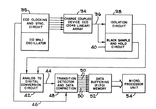
With reference to Fig. 2, a functional block
diagram of the camera fiensor 22 i6 illu6t~ated. The
vertical column of CCD units 34, con6isting of a 2048
pixel linear array in the illustrated embodiment, is
2~ connected to receive clocking or timi~g signals from the
clock and sync circuit 35. Clock circuit 35 includes an
06cillator running at a frequency of at least about one
MHz, and 10 MHz in the illustrated example, in order to
provide pixel scanning in about 200 micro6econd6 and 100
micro~econds for reset operation. The CCD units that
are commercially available are capable of running at
clock frequencies as high as 40 MHz. Thu~, pixel scan
during a 300 microsecond sampling ~can after
conditioning, is u6ed to produce an analog information
signal which contains a transition relating to the
precise position of an edge poin~ on an object or part
which is ~eing conveyed.
2~5~7~
From the column of CCD units 34 which eac~
functions as a pixel. an output signal on lead 36 i~ in
the form of an analoq signal voltage (6ee Figs. 4 and 5
containing sequentially obtained voltaqes of a first
amplitude for shadowed pixels and a second low amplitude
for those pixels receiving light from light source 24.
The analog information is a serial bit stream of uniform
length and is transferred serially at the clock rate to
a voltage follower that serves as an isolation circuit
3B and to a black sample and hold circuit ~0 which
produces a voltage level reference ~ignal from pi~els
that are blocked from receiving light. This provides a
reference signal which holds the analog signal at a
controlled DC level and may be u6ed as one input to
1~ circuitry associated with an analog to digital
conversion circuit 42.
The output signal on lead 44 is applied to the
transition detector and data compaction circuitry 48
which will be described in connection with Fig. 6. On
lead 46, a clock signal from the clocking and ~ync
circuit 35 i5 applied to maintain synchronization
between the data com~action unit 48 and the 6cannir~g
means that is part of the charge coupled device array 34.
The output signals from the data compaction
device 48 on leads 50 i~ in the form of a single bina~y
number for each transition from the analog to digital
conversion circuit and is applied to the memory 52 which
serves as a buffer to collect all of the data for a
particular object 12, 14 or 16 on the conveyor surface
on a first in, fir~t out basis. The microproces60r unit
54, which may be any suitable type that is commercially
available, may ~tart to process the output signals as
soon as the memory SZ begins to receive valid object
data.
The camera sensor 22 is thus ~ynchronized with
a counter în the data compactor 48 by means of the
clocking and ~ync circuit 35. The memory 52 for data
2~.307t 1
- 7 -
buffering may have a 64X or even smaller capacity for
object~ of the type ~entioned above. AS poin~ed out
above, low cost commercialiy off-fihelf a~ailable
components have a capability to operate up to a 10 MHz
data rate in a reliable fashion thereby providing a low
cost hardware product.
With reference to Fig. 3, there illustrated a
round of ammunition which has a cylindrical cartridge or
casing 56 that i8 supported on a conveyor surface 18 and
a projectile 58. Fig. 4 contains a group of waveforms
taken alcng line 4-4 of Fig. 3 and Fig. 5 contain6 a
group of similar waveforms taken along line 5-5 of Fig.
3. Fig. 4 waveforms are taken at a position
corresponding to scan 120 whereas, the Fig. 5 waveforms
are taken at scan 800.
In ~ig. 4, the wa~eform of the amplified analog
signal ~tarts at time 0 in a black condition because of
the conveyor 18. At pixel 30, which corresponds to
count 30 in a counter, light is detected thereby
starting a negative going digital pulse and a positive
going edge detector pulse 60. At pixel 100, the lower
edge point on the silhouette of the projectile 58 is
effective to block light and create a further edge
detector pulse 62. At pixel 500, the light is again
detected, thereby sau~ing a third edge detector ~ignal
64 to be generated. Finally, at the top of pixel linear
array and pixel 2048, the scanner no longer produces a
signal and an end of scan tran~ition detector pulse 66
is qenerated~
A conventional binary counter capable of
counting up to at least 2048 at the clock frequency is
synchronized with the scan of the 2048 pixels in the
camera sensor as indicated at the bottom waveform of
Fig. 4. The clock is reset to start at zero as the scan
starts so that count values of 30, 100, 500 and 2048 are
stored in the memory 52 of Fig. 2 as determined by the
time of o~currence of edge detector pulses 60, 62, 64
and 66.
- 8 - 2030711
Fig. 5 shows the corresponding waveforms that
occur at ~can 800. Since the lowe~t point on the
cylindrical casing 56 rests on the conveyor surface 18,
the lowest 1499 pixels in the linear array are dar~ and
the first transition occurs with pixel 1500, which is
aligned with the upper edge point of the cartridge
casing 56 at scan position 800.
The edge detector pul6e 68 is generated in
re~ponse to the tran~ition at ~ixel 1500 and causes the
count value of 1500 to fall through the memory 52 to its
output terminal~. A similar edge detecto~ pulse 70
occurs at count 2048. Thereafter, a master re~et pulse
is generated. The counter6 are reset to a zero count by
a counter reset signal which is synchronized with the
beginning of the next scan of the pixels.
Fig. 6 shows one psefe~red em~odiment for
converting the digital signals of Fig6. 4 and 5 into
count values that are supplied to the microprocessor
unit (MPU) 56. The digital signal from Fig. 4, in the
form of incoming ~erial binary bit, is applied to
terminal 80 of a negative and positive edge detecting
network that detects change6 in the binary state and
i~sues for each positive or negative edge a 50n sec.
pulse on lead 82. At a 10 MHz clock frequency, the
~canned informatio~ data and clock counts are ~eparated
by lOOn sec. The 50n sec. pulse i6 u6ed to gate on the
memory unit 52 ~Fig. 2) which includes FIF0 registers 84
as illu~trated in Fig. 6. The three ~inary counter
registers 86 that operate with clock signals on lead 46
are reset ~y a counter reset signal on lead 88. The
count value on lead~ 50 is con6tantly presented to the
FIFO registers 84. However, the count values are
allowed to drop through the FIFO regi~ter6 84 only when
an edge detector pulse on lead 82 is present. In this
example, the count values of 30, 100, 150 and 2048 are
~tored.
- 9 - 2 0 5 0 7 ~ 1
When a count value fall6 through the FIFO
registers B4, the FIFO ifisue6 an output ready signal to
MPU 5q on lead 92. When the MPU ~ees an output ready
signal, it is6ue6 a shift out signal on lead 94 to FIFO
registers 84 which releases the count value immediately
to the MPU 90. The data at this point is then coded
object image intelligence. Thi6 handshaking continues
throughout the entire scan cycle and 6equentially
throughout all scans of a object.
As is evident from the foregoing. for the scan
120, only four count values are proces6ed and 6tored
rather tl~an 2048 bit~ of scan information. Other scans
such a6 scan 800 may have only two count values that are
processed. The number of scan6 may be decreased where
1~ less re601ution in the horizontal direction is
acceptable thereby further reducing the proces6ing
time. This compaction of data increase6 processing
speed and reduce6 memory 6ize requirement6 without
6acrificing re601ution of the 6ilhouette image.
While only a single embodiment hag been
illu~trated, other modification6 and variations will
become apparent to t~o6e skilled in t~is art. The
illustrated embodiment ha6 a degree of sophi6tication
which can be simplified for le66 demanding
application6. It i6 therefore intended that the
variations and modification6 which fall within the 6cope
of the appended claims and equivalents thereof be
covered thereby.