Note: Descriptions are shown in the official language in which they were submitted.
SCM/39ss e
MOVING VEHICLE TRANSPONDER
F1eld of the Invent10n
__
Th1s ~nventton relates to tag transponders, part~cularly
though not exclusively for attach~ng to veh1cles.
Background Art
A system has been devised which allows road toll fees to be
collected automatically.
The syste0 compr1ses an 1nterrogator dev ke bur1ed ~n the
carr~ageway and a transpond~ng tag f~tted to vehicles.
When a su1tably equlpped veh~cle approaches a toll po~nt
~ts presence ~s detected by an ~nduct~ve loop detector (s~m~lar to
that used at traff~c 119hts) and the ~nterrogator ls energ~sed. Thls
dev~ce transmlts a signal at 915 MHz to the veh~cle, the transmlsslon
carr1es a code wh~ch 1s recogn~sed by the vehicle Utag" as a command
to turn on its transmltter. The tag transmitter then sends a coded
s~gnal to the interrogator ~n the carr1agewdy~ The coded lnformat~on
contains the vehlcle reg~strat~on number. It ls therefore poss1ble
to collect toll fees without the need for manned toll booths and
wlthout the need for vehicles to slow down so that money could be
transferred.
It w~ll be understood for the purposes of th1s
speclf1cat10n, "transponder ta~" ls 1ntended to mean a unitary dev~ce
wh~ch lncludes elements necessary for 1ts operat10n ~n rece1v~ng
radiated slgnals an~ transml~ting signals tn response ~hereto.
Summary of the Inventlon
It is an object of the present lnvent~on to prov~de a
transponder tag wh~ch ls of a part1cularly simple, lnexpens~Ye and
rel~able construct~on.
The present 1nvent~on ~s lntended to operate ~n the UHF
range, and speciflcally 915 MHz. HoweYer for the purpose of th~s
specif~cat~on "UHF range" ~s ~ntended to mean any frequency
below 2 GHz and excludlng frequencles ~h~ch would normally be
regarded as mlcrowave.
The present ~nvent~on prov~des a transponder tag operat~ve
in the UHF range and 1ncludlng a substrate of dtelectric mater~al
havlng formed on one slde a conduct~ve surface prov1d~ng a ground
plane and a dlpole antenna, a slot line with~n the ground plane
forming a balanced antenna feeder and leading to the centre of the
d~pole antenna, and the substrate having mounted on the s~de of the
substrate opposite to sa~d one side a transm~ss~on line feeder
pos~t~oned for electromagnetic coupl~ng wlth sald slot l~ne, the
transm~ssion llne feeder belng coupled t~ transce~ver clrcuit means
and processing means mounted on the opposlte s~de for perform1ng a
transponding function.
Thus in accordance w~th the ~nvention a transponder of
part~cularly s~mple construction ~s provided operating ~n the UHF
range ~ncludlng an antenna and balanced feeder arrangement formed ln
a partlcularly s~mpte manner on oppos~te s~des of a dlelectr~c
substrate.
As preferred the dipole antenna ls formed by remo~lng for
example by etching selected parts of sa1d conduct~ve surface~ leav~ng
a str~p def~nlng a d~pole antenna wh~ch ~s connected to the ground
plane at the central reg~on of the strlp.
As preferred the transm1ss~on llne feeder comprlses a
conductlve strlp, /4 long and term~natlng at a pos~t~on generally
oppos~te the slot line for max~mum coupling to the slot llne.
The transcelver means campr1ses an osclllator coupled v1a a
buffer (power) ampl~f~er to the transm1ssion l~ne feeder, the
--3-
collector of an RF trans~stor of the ampl~fler belng dlrectly coupled
to the feeder. As preferred the osc~llator and ampl1f1er are CW
modulated by switching of the power supplled to the osc~llator and
ampllf~er by means of output data signals from the processor.
The receiver ~s capacitlvely coupled to the feeder w~th the
base of a recelver translstor be~ng directly connected to the AC
coupllng. The recelver demodulates recelved RF signals and provldes
the demodulated data to the process~ng means, whlch preferably
comprlses a processor and memory ~ncludlng stored programs, all
provlded ln a slngle ASIC.
Br~ef Descr~ptlon of the Drawln~s
A preferred embodlment of the ~nventlon w~ll now be
descrlbed wlth reference to the accompanylng draw~ngs, whereln :-
F~gure 1 is a block diagram of the transponder accord~ngto the ~nventlon;
Flgure 2 ~s a circu~t d~agram of the transce~ver of
F~gure l; and
Flgure 3 is a plan vlew of the transponder show~ng the
antenna and antenna feed arrangement.
Descrlptlon of the Preferred Embodlment
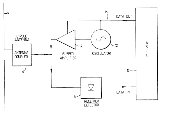
Referrlng now to thè drawings Figure 1 ~s a block dlagram
of the tag accordlng to the inventlon and shows a d~pole antenna 2
coupled vla an antenna coupler 6 to a receiver detector 8 whlch
demodulates data received by the antenna and passes the demodulated
data to a data processor 10 formed as an ASIC. Output data provlded
by processor IO ~s coupled to an RF osclllator 12 wh~ch osclllates
a 915 MHz and to a buffer (power) ampllf~er 14 whlch amplifles the
osclllator slgnals and feeds the signals to antenna coupler 6. The
data on output llne 16 from processor lO modulates the osc~llator and
buffer amplifer ln a CW modulation mode wherein both the osc~llator
and ampllfler are swltched on/off d7rectly by the output data.
Referring now to Flgure 3, thls ~s a plan v~ew of the tag
transponder comprls~ng a substrate block 30 a relatlvely low
dielectric value polyester res1n and having on 1ts upper s~de a
conduct1ve surface 32 (for example copper) coated thereon. The
surface 32 forms a ground plane and port~ons of the surface 32 are
removed as at 34 to provlde on one s~de of the surface a dipole
antenna strip 36 hav~ng an ~nput ~mpedance of 75 ohms at 1ts centre.
A slot l~ne 38 ~s formed ln the ground plane extend~ng from the mld
po~nt of the antenna 36 and forming a right angled bend as at 40.
On the other slde of the d~electr k body as ~nd~cated ~n dotted
l~nes, the electr~cal components ~ndlcated ln F19ure 1 are mounted
as at 42, preferably by means of surface mount technology on an
array of solder bumps. The electron k components 42 are coupled to
the antenna by means of a transm~ss~on llne 44. Transm~ss10n l~ne
44 ~s formed as a str~p of conductlve metal coated on d~electr1c
block 30 and hav1ng a length ~/4 w1th the free end of the strlp 46
terminat~ng close to a pos~tlon d~rectly opposlte slot l~ne ~8.
The end of str~p 46 is coupled via a capac~t~ve coupl~ng 48 to
ground plane 42. This arrangement prov~des a maxtmum
electromagnetlc coupl~ng between the end of str~p 46 and slot line
40, the radlat~on be~ng coupled to slot l~ne 40 and then be~ng
conduct~ve ~n a balanced feed arrangement on e~ther stde of the slot
llne to the d~pole antenna to provlde a balanced feed to the dipole
antenna.
The dlpole antenna is printed on the same PWB (printed
w~ring board) as the tag electronics.
Referring now to Flgure 2, this shows a c~rcuit d~agram of
the transce~ver arrangement as comprising d rece~ver or detector 50
coupled to transmisslon l~ne 44 v~a a capac~tance 52, the base of an
RF detector trans~stor 54 being directly coupled to capac~tor 52.
The collector of translstor 54 ~s coupled to the base and, vla a
d~ode 56, to the emitter of a further trans1stor 58. A tun~ng
circuit for the detector ~s formed by the quarter-wave transmlss~on
line 449 while trans~stors 659 66, capacltor C1 and ~nductor Ll
provide act~ve blas for the detector trans~stor 54. The
comb~nation of trans~tor 54 dlode 56 and trans~stor 58 provlde a
-5--
means of demodulating the data from the input RF slgndl and the
demodulated data ls fed to processor 10. Processor lO responds to
the lnput data by provlding data on output llne 16 for modulation of
an oscillator 12 compr1slng a trans~stor 60 and a resonant c1rcuit
arrangement L2, C3, C4, the frequency of osc111at~on be1ng
determlned by a m1cro strip 62. The osc111ator 1s coupled to buffer
ampllf1er 14 compr1slng an RF transistor 64 coupled 1n common base
mode to osclllator 12 and having lts collector dlrectly coupled to
feeder 44.
The processor c~rcu~t 10 ~5 powered by a llth1um battery
(not shown) and the battery and transponder tag are housed ~n an
overall plastics encapsulatlon.