Note: Descriptions are shown in the official language in which they were submitted.
~ 23~ PCT/~B90/~
2 ~
DISPLAY.
The present invention relates to a display.
A known type of display compris~ a static base unit and
a rotating unit driven by a motor. The rotating unit
carries a plurality of light emitting d~odes (LED's)
which are controlled during rotat~o~ so as to provide a
display image.
EP 0 026 762 discloses a display of ~hiC type in which a
rotating two dim~nsional array o~ LE~'~ sw~ep~ a
cylindricaL volume and the L~D 's are controlled so as to
defi~e a cylindrical thr~e dlmensional array of picture
elements (pixels). Data for co~rolling illumination of
the pixels is sent in serial form from fixed electronics
in the base uni~ via a~ rared link ~o rota~ing
electronics in the rota ing unit. The rotating
elec~roni~s essentially comprise a decoder for
illuminating each L~D of the array in s~quence, with no
da~a storage bein~ provided in the rota~ng unit. Thus,
only one L~ a~ a time can b~ illuminated.
GB Z 093 617 and EP 0 156 544 di close di~plays of this
type a~ whlch two diametrically opposite vertical columns
o~ ~ED'8 ~w~ep a common ~ylindrlcal display surface and
the LED'~ ar~ ~ontroll~d so ~ to de~ine a cyllndrical
two, dimensional array of pix01s. The rotating unit
con~ain~ enough ele~ronic~ and ~ory ~or all of the
LED's to be controlled simultaneou~ly and for data to be
stored for all of ~he pixel~ to provlde one complete
image. In order ~o: charlge the display~d imag~, a
connection has ~o be established with ~che rotating unit
so ~hat n~w data can be writ~en in~o the memory. Durlng
such reprogra~uning, ~che display cea~e~ to, function as a
display un il the old data have be~n replaced by the new
.
WO 90~1235~ P~/GB~/00~64
2 ~
data. Thus, dispLay images cannot be changed during
normal operation of the display. This make~ image
updating and animation dif~icult or impossible and
requires expert or tra~ned personnel to reprog~mme the
display .
Another pr~blem with knowll display~ of this type is that
the light output i~ relativ~ly low. Thus, shaded
locations are necessary f or viewing such displays .
According to a first aspect of the invention, there is
provided a display comprising a static unit a~d a moving
unit, the moving unit carrying a plur~lity of light
sources and being arranged to move so that the light
sourceC perfonm a repea~ed mov~ment, the moving uni~
including a memory for storing data for providing a
plurality of displayed images and control mean for
control~ing the light sources so a~ ~o displ y at least
ona selected image at a time.
The moving unit is prefer~bly a rotating unit and the
ligh~ source~ are pre~erably arranged as a plurality of
co}umns parallel to the axis of rotation. The light
sources ar~ pr~erably ligh~ em~tting diode~.
~h~ s~at~c unit i5 prefera~ly arrang~d to co~municate
w~th ~he moving unit by mean~ of a communicatlon link,
such ~8 a ro~ry transforner. Preferably the static unit
co~a~n~ a further memory ~or storing da~a ~or a
plurali~y o~ ~ur~her displayed imag~ and transmission
means for tr~smi ting ~he data to th~ ma~ory and the
con~rol mean~ of the moving unit via the co~munication
link.
It is ~hus possible to provide a display which perm ~ s
sev~ral ~m~g~es to be displayecl ln a de~ired sequence, f or
~) 90/12354 PCI/GB90/00564
2 ~ g l
instaslce . o a~s to change the image~ or so a~ to prov~de
animated images.
According to a second aspect of the irlvention, there is
provided a display comprising a ~tatic unit and a
rota~ing unit, the rotating unit carrying a plurality of
columns of light sour~es arranged to sweep a ~ommon
cylindrieal sur~ace, the liyht sour~es of each colwmn
being oriented parallel to each o~her at an angle to a
radius ~rom the axis of rotation through th0 column and
the light source of ~ leas~ two of the columnR being
oriented at respective different angles.
In g~ner~l, light sources such as light emittlng diodes
emit most of ~heir light ~orwards along their optical
axis, with the llght intensity falling with incr2asing
angle ~rom the axis. By varying ~he orientatlons of the
columns, it is possible to provide a oylindrical image
wh~ch remain~ vlsibl~ close to ~he extreme~ of the
cylindric~l surface which are visible from any one point.
At leas~ two of the COlUmn8 may be o~fset relative to
ea~h other paralle} ~o the ro~ational axi~ so as to
provide interlacing.
According ~o a third aspec o~ th~ inven~ion, th~re is
provld~d a d~splay, comprising a static unit, a rotatlng
~un~t c~rrying a plurality of light source~, a motor for
drlving th~ ro~ati~g unit, and a con~rol circul~ for
controlling the ~p~ed o~ the motor, the control circult
comprising means for repeatedly pre~etting a counter to a
pre~e~ valu~, m~ans for s~epping the coun~r towards a
pred~termin~d value at a predetermined rate for a period
rela~ed to the pe~iod of rota~ion of th~ motor, and means
for ~upplying increased power to th~ mo~or when the
counter reache~ the predetermined value.
WO 90/12354 PCr/GB90/00564
4 2 ~
Such a syctem provides highly accura~e motor Rpeed
control and, by using stable or similar clocks to control
the ligh~ sources a~d the prede~ermined rate, dispenses
with the need for any kind of synchronisation between the
static and rotating units.
According to a further aspect of the invention, there is
provided a display according to any combination of the
first to third aspects of the inve~tion.
According to ~ fi~th aspect of the invention, there is
provided a motor speed controller compxising means for
repeatedly presetting a counter to a pre~et value, means
for stepping the counter toward a pxedetermined value at
a pred~termined rate ~or a period related to the motor
rotation period, and means for supplying increa~ed motor
power when the counter reaches the predeter~ined value.
The inve~tion will be ~urther de~crib~d, by way of
example, with r~erence to the accomp~nying drawings, in
which:-
Figure 1 i~ an external view of a display constituting a
: pre~erred embodiment of ~he invention;
::
Figur~ 2 shows the di play o~ ~ gure 1 with ~ch~ caseremoved;
Figure ~ i~ a side view of part o~ the display of Figure
lj,
Figure 4 is a plan view of ano~her part of ~he display of
Figure 1;
:
Figure 5 i~ a diagrammatic plan view o~ th~ part of the
di~play ~hown i~ Figur~ ~;
~ ~/123~ PCT/GB~0/~
2 ~
Figuxe 6 is a block schematic diagram of the display of
Figure 1;
Figure 7 is a circuit diagram of a display card of the
display of Figure 1;
Figure 8 is a block circuit diagram of a rotating control
CiICUit of the display of Figure l; and
Figure 9 is a block circuit diagram o~ a motor control
arrangement of the display of Figure 1.
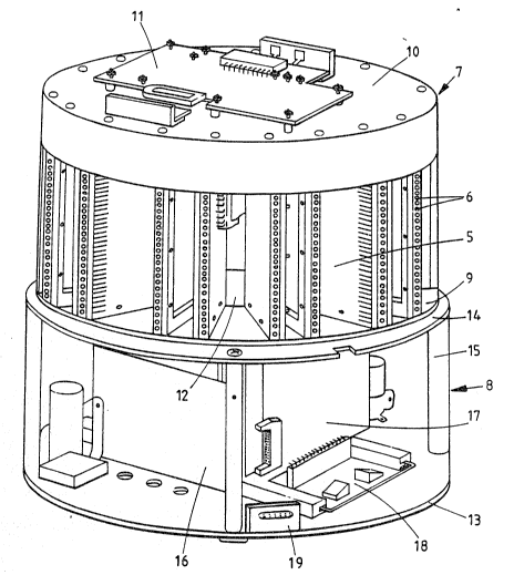
The display 1 shown in Figure 1 comprises a cylindrical
case having opa~ue upper and lower parts 2 and 3
separated by a transparent middle part 4. A plurality of
display cards 5 is visible through the transparent part
4, with each display card havi~g at its radially outer
edge a vertical column of thirty two light emitting
diodes 6.
As shown in Figure 2, the display cards 5 are mounted on
an upper unit or carousel 7 which is rotatably mounted on
a lowsr base unit ~. The cards 5 are supported hetween a
lower carousel plate 9 and an upper carousel plate 10,
which Garrie8 display control electronics on a control
card 11. The carousel 7 is mounted on th~ shaft of a
dr1ve motor 1~ which is fix~d to the base unit a . The
base unit 8 has a base pla~e 13 rigldly connected to an
upper plate 14 by spacers 15. The p~ate 13 also carries
var~ous circuit boards, such as 16, 17, and 1~, and a
serLal por~ inpu connectox 19.
As shown in Flgure 3, the base plate 13 provides a
moun~ing for a support plate 20 which is mounted by means
of pillars 21. Th~ motor 12 is moun~ed to the support
plate 20 by means of pillars 22.
w~ ~/123~ PCT/GB90/~
The m~tor 1~ has an output sh~ft 23 which extends abov~
and below ~he motor. The shaft 23 is made of metal or
o~her electrically conductive material and is provided
with a slip ring 24 which co--operates with a pair of
brushes mountPd in brush holders 25. The brushes are
connected to the common ox earth line of a power supply
mounted in the base unit 8.
The upper part of the motor shaft 23 is provided with
another slip ring 26 which is electrically insulated ~EDm
the shaft. The slip ring 26 co-operates with a pair ~E
brushes mounted in brush holders 27. The brush holders
27 are fixed to a support plate 28 which is fixed by
pillars 29 to the top of the motor 12. The brushes co-
operating with the slip ring 26 are connected to a
positive voltage output of the power supply in the base
unit. The motor shaft and ~he slip ring 26 are connected
to a power supply unit of the carousel 7 as will be
described hereinafter.
A rotary transformer is pro~Jided for transmitti~.g data
from the base unit 8 to the carousel 7. The r: :ary
transformer comprises a fixed assembly 30 mounted on the
support plate 2~ and a ro~ating assembly 31 mounted on a
carousel support hub 32 provided with a ~oss 33 and fixed
to the mo or sh~ft 23. Each of the parts 31 and 32 of
the rotary transformer comprises a ferrite ring
~upporting a coil or winding.
Fi~ure ~ shows the arrang~ment of display cards or
circuit boards 5 mounted on the carou~el support hub 32.
Each circuit board S is provided with a support frame 34
for support and for connection to the hub 32. The
columns of light emit~ing diodes 6 are mounted on LED
; brackets 35. Sixteen display boards 5 are provided and
are arranged as two groups of eight boards with the first
set being conn~cted to a ribbon cable bus 36 and the
, 90/12354 pcr/GB9o/~os64
$ ~ ~
.
second ~et being conne ::ted to a ribhon cable bus 37 .
Display board collnec:tors are shown at 3~ and power supply
and data connections rom 'che slip r~ ng~ 24 an~ 26 and
f rom the rotary tran~:f ormer secondary winding cr part 31
are indicated at 39, 40, and 41.
Figur~ S illustrates diagraaunatically the po~itions and
orien at ions of th~ column~ of ligh~ emittirlg diodes with
respect l:o the axi~ 42 of rotatiorl of the carous~l. Th~
columns; o~ ligh~ emitting diodes are labelled by numbers
f rom 1 to 16 inside circles . The COlllIlU19 are equi-
angularly spaced 2!bou~c the circun~erence of the carousel
such that the arlgle a between each adjacent pair of
columns is equal to 22~. The arrows in Figure S
indicate the optical axis of each light emitting diode ir
the columns, with the axes o~ the light emit~ing diodes
in each column being parallel. Thus, the light emitting
diodes ln the colulM labelled "1" are orien'ced at an
angl~ of ~ anti-clockwise with respect to a radius
pas3ing through the column, whereas the axis of the
column "2" is displaced by an angl~ ~ clockwise with
resp~ct to the radius through the colu~n. The
orientations of the axes of the other columns are as
shown in Figure S and, in a pre~err~d embodim~nt, the
angl~ 0 i~ 12 and the angle ~ i~ 48. Such an
arrangeme~ otnpensate~ f or the li~ited angular
dl~per~t or~ o~ llght from the ligh~ emitting d~odes to
eith~r ~ida~ of ~he optical axls, and par~its light f rom
~h~ display to be rec~ived by a vlewl3r for substantially
the whol~ of thQ~ part o~ th~ cylindri~l surf~e
described by ~chQ column~ o~ light eMit~cing diodes f aclng
th~ viQwar. In practice , the purtion o~ th~ cylindrical
surface whl~h is visible and fro~ which li~ht can be se~n
is less than but close to 1~0, for instance about 160' .
In order ~o provide a mul~ colour im~g~, columns of red
light emitting diodes and column~ of green light em~ n~
~/123~ PCT/GB~/~
diodes are provided. Thus, the columns "l", "4", "6",~
"7", "9", "12", "14", and "15" consist entirely of red
light 2mitting diodes, whereas the o~her columns consist
entirely of green light emitting diodes.
Further, the light emitting diodes in all of the columns
ar~ arranged to have a common pitch and the columns "l",
"2", "3", "6", "7", "8", "l2", and "l3" are arranged at
the same height so that the n-th light emi~ting diode in
each of these columns follows exactly theOsame circular
path. The remaining columns are also at;,~e same height
as each other but are displaced upwardly--with r~spect to
: the above mentioned columns by half the pitch of th~
light emitting diodes. Thus, the sixteen columns provide
an interlaced display to improve the vertical resolution
of the display.
Each of the columns "l" to "16" can thus be displaced
from the local radius by one of tw~ angles and in one of
~wo directions, can be one of two colours, and can be in
one o~ two interlaced groups. This gives sixteen
posslble combinations of parameters and all sixteen
. combina~ions are present in the sixteen columns of light
emitting diodes.
As will b~ d~scribed hereinafter, the display i~ arranged
to p~ovide 512 discrete circumferential picture elements
(pixels). In order ~ox the circ~mfere~tial display
: definition to b~ the same as the vertical definition, the
pitch of the light emit.ing diode in th~ columns is made
equal to the circumference divided by ~56 (th~
interlacing of the display giving the same vertical
resolu~ion as circumf erential resolution ) .
~
Figure 6 is a block schematic diagram of the electronics
in th~ sta~ic or base unit 8 and the rota~ing unit or
~123~ PCTIGB90/M~4
carousel 7. A single block 5 represent~ th~ sixteen
display cards.
A mains input co~nector 43 is connected to a power supply
unit 44 w~ich supplies power to the electronics in the
base unit 8 and, via the slip rings 24 and 26, in the
carous~l 7. In addition, the mains input connector 43 is
con~ected to a motor speed control circuit 45 which
controls the supply of power to the motor 12 and controls
motor speed by means of a servo loop which receives motor
speed feedback signals from a variable reluctance pick-up
46 whi~h, as shown in Figure 3, comprises a fixed sensor
47 and a toothed wheel 48 mounted at the bottom of the
motor shaft 23.
The data input connector 19 is connected to a
receiver/decoder, for instance complying with the RSZ32
or RS432 standard. The output of the receiver 49 is
connected to a sequence control logic circuit 50 which
receives timing signals from a timer 51 controlled by a
crystal oscillator 52. The sequence con~rol logic
circuit 50 has an output conn~cted to a data transmitter
53 which sends data via the rotary transformer 30, 31 to
the carousel 7. The sequence control logic circuit 50 is
also conn~cted to a removable da~a module 54 which
compris~ a sequence ran~om access memory 55, a page
store r~ndom access memory 56, and a rechargeable battery
57 ~or m~intaining the contents of the memories 55 and 56
when the display is disconnected from the mains.
The ~arousel 7 comprises a da~a receiver 58 which
receives data from the rotary transformer 30, 31 and
which has outpu~s connected to a pag0 control circuit 59,
a timing ~raln and control logic circuit 60, and display
data random access memory 61. The logic circuit ~0 is
connec~2d to outputs of the page ~on~rol circuit 59 and
the memory 61, and receives clock pulses from a crystal
~ ~/12354 PCT/GB90/~K~
lo ~ $~
oscillator 62. The logic circuit 60 and the memory 61
are connected to the display cards 5 by the buses 36 and
37 shown in Figure 4.
The display operates as follows. When ~he display is
first actua~ed by supplying mains power to the input
co~nector 43, the motor 12 rotates the carousel 7 and
accelerates until a preselected speed of rotation is
reached. The mo~or speed control circui~ 4S then
stabilises the ro~ary speed of the carousel at ~he
preselected value. The speed is not actively
synchronised in any way with the display electronics in
the carousel 7, but speed stability is based on the
stability of ~ crystal oscillator which is substantially
identical to the crystal oscillator 62 which controls
display timing. The crystal oscillator for the motor
speed control circuit 45 may be provided by the crystal
oscillator 42 or may be provided i~depe~dently.
Meanwhile, display data are sent from the data module 54
by the sequenc~ co~trol logic circuit 50 via the data
transmitter 53 and the rotary transformer 30, 31 to the
carousel 7, whose elec~ronics receive power via the slip
rings 24, 26 from the power supply unit 44. Display and
con rol data are received by the data receiver 5~ and are
stored in the display data memory 61. The timing chain
and control logic 60 then cause data to be supplied .rom
the me~ory 61 to the display cards 5 with appropriate
timings ~o provide the desired displayed image.
Th~ cylindrical display surf ce swept by the columns- of
light emitting diode~ 6 is divided into 512
circum~erential by 64 vertical pixels and the memory ~
contains data ~or providing four comple~e displays, each
using all of the pixels and referred to hereinafter as a
"page". At any one time, one of the pages is hidden or
blanked and does not affect the display but instead is
, .
' ~/123~ PCT/~9~
$ ~
11
available to receive fresh display data from the base
unit B~ The other three pages provide three display
images which are superimposed so as to provide ~ complete
image or "band".
The data for each pixel may control it such that it is
off, green, rad, or yellow (green and red). Data held in
the page control circuit 59 allows each of the pages to
commence at a selectable circumferential position.
The display timing is ~etermined by the crystal
oscillator ~2 and a static image relies on substantially
identical timing control within the motor speed control
circuit 45. However, a rotating image may b obtained by
selecting a variation in speed by means of the motor
speed control circuit 45 or by periodically altering the
circumferential starting po~ition of one or more of the
displayed pages. A degree of animation may also be
achieved by loading f resh pages from the data module 54
into the display data memory 61 at a speed sufficient to
provide an apparently changing image, or by displaying
only one of the four pages stored in the memory 61 at a
time and in sequence.
In a preferred embodiment, the circumferential starting
position for each page can be selected as any one of 256
cirsum~erent~al co}umns of pixels. The starting point
thus has hal~ th~ circumferential resolution of the
display, but this has been found adequate in practice
while relievin~ design and ~echnical requirements on the
elec~ronics of the display.
Figure 7 i~ a circuit diagra~ of one of the display cards
5. The card is implemented with high-speed TTL and CMOS
integrated circu~ts of the 7400 series, available from
various manufacturers, and the type numbers for the
individual integrated ~ircui~s will be given hereinafter.
W~ ~0/1235'3 PC~/GB90~(10564
12 2 ~
For the sake of clarity, multi-line connections or buses
are shown in the circuit diagrams as a single line with a
short crossing line and associated number indicating the
number of lines or channPls making up the connection.
The thirty two light emitting diodes 6 are arranged as
four groups of eight, with each group being controlled by
a respective octal latch/driver 63 to 66 of the type
74LS374. The latch/drivers have latch enable inputs
which are connected toge~her and to a display card input
67 for receiving an upda~e conkrol signal UD. Each o~tal
latch/driver comprises eight identical latches, each of
which is controlled by the enable input and i5 capable of
supplying sufficient current to drive the corresponding
light emitting diode 6.
The data inputs to each latch/driver 63 to 66 are
connected to the outputs of set/rese~ flip/~lops 68 to
75, each of which comprises a quad set~reset flip/flop of
type 74LS279. The flip/flops 6~ to 75 have clear inputs
which are connected to a display board input 76 for
receiving a clear signal CLR.
The set input~ of the flip~flops 68 to 75 are connected
to the outputs of four octal buffer tri-state line
driv~rs 77 to 80 of type No.74~G244, whose data inputs
are connected in parallel to a common 8-line bus for
receiving display data signals D0 to D7. The oc~al
bu~ers 77 to 80 have enable input~ connected ~o the
outputs of AND gates 81 to 8~, respectively. The AND
gates 81 to 84 have first inputs connected to receive
st~obe signals S0 ~o S3, respectively, and second inputs
conneote~ toge~her to receive a board enable signal 3E.
The input si~nals UD, CLRt BE, S0 tO S3, and D0 to D7 are
rec~ived from the ~us 36 or 37, depending on whether ~he
,
7 ~/1~ ~ PCT~GB~/~
13
particular card 5 is a member of the group "1" to "8" ~r
"9" to "16". In addition, a supply line Vcc and a common
line (not shown) are connected to the respe~ti~e bus,
which provides power to the display card 5.
In order to write new data ~or controlling the llght
emitting diodes 6 to each display card 5, a board enable
signal ~E is supplied to the selected card. The gates 81
to 84 are there~ore opened and the board i ready to
; receive the strobe signals S0 to S3. Data D0 to D? are
supplied to the octal buffers 77 to 80 for controlling
the light emitting diodes connected to the octal latch
63. The strobe signal S0 is supplied so as to enter the
data in the octal buffer 77, and hence into the
flip/flops 68 and 69.
Data for the next group of eight light emittlng diodes is
then supplied on the bus as bits D0 to D7 and the strobe
signal S1 is supplied so as to enable the octal buffer 78
and enter ~he da~a in the flip f}ops 70 and 71. This
process is repeated until the data for one column of
~: ~ pix ls for one of the three pages to be displayed has
b~en antered in the flip/flop3 6~ to 75. The whole
process i5 then repeated for the same colu~n of pixels
or the second page to be displayed, without clearing the
flip flops 6~ to 75. The new data is therefore
~e~f~ctively superi~posed on the data ~or th~ previous
page . The process is then repeated again f or ~he ~hird
page, aft~r which the board enable signal }3E is removed.
;: ~ : : : :
:Thi~ proces3 is repeated for each of boards "1" to "8"
a~d simultaneously or boards "9" to "16" via the two
data buse6 36 and 37 so that ~he data for displaying the
next six~een columns of pixels ara enterPd in the
flip/flops of all sixt~en display boaxds. At the end of
~ ~54 P~T/GBgO/~
2 ~
14
this cycle, the update signal UD is supplied to all
sixteen boards so tha~ the new data axe written into the
latches 63 to 66 simultaneously on all boards and the
sixteen next circumferential columns of pixels ar~
displayed in place of the previous on~s. A clear signal
CLR is then supplied to all sixteen boards so as to reset
all of the flip/flops 68 to 75 in readiness for r~ceipt
of the data for the next columns of pixels.
The data receiver 58, the page control circuit 59, the
timing chain and control logic circuit 60, the display
data random access memory 61, and the crystal oscillator
62 are shown in more detail in figure ~.
The carousel 7 has a local power supply unit 85 which
receives power from the slip rings 24, 26 and supplies
power to the electronics shown in figure 8 and to all of
the display boards 5.
The rotary transformer 30, 31 is connected to a frequency
shift keying (FSX) demodulator 86 whose output is
conn~cted to a decode logic circuit 87. The logic
circuit 87 has an ou~put connected to a data input of th~
memory 61, and further outputs whose connections will be
described h~reinafter.
Th~ crystal o~cillator 62 supplies clock pulse~ to a 16
bit binary cou~ter 88 whose leaæt significant bit outputs
are shown at the left with the slgnificanc~ of the bi~
outputs increasing progressively to the right. Thus, the
two least significant bi outpu~ are oonnected to inputs
of a 16 bit 2-to-1 multipl~xer 89 a~d fo th inputs of a
decoder 90 whi~h decodes ~he.two bits to 1-of-4 outputs
which provida the strobe signals S0 ~o S3 for the display
boards. The next two co~nter ou~puts pro~ide a two bit
''~ ~/1~3~ PCT/GBgO/M~
code to the multiplexer 89 and indicate which of the four
pages making up a band is currently being addressed.
These outputs are also connected to a decode logic
circuit 9l and to a 4 by 8 bit position random access
memory 92 and a 4 by ~ bi~ colour random acc~ss memory
93. The next three outputs of the counter 8~ are
supplied to a four bit adder 94 and to a decode logic
circuit 95. The three bits at these outputs indicate the
display boards of the first and s~cond groups which are
currently b~ing addressed, and the decode logic circuit
95 decodes these bi~s and signals from t~e decode logic
circuit 9l so as to provide l-of-8 outputs constituting
eight board enable signals ~E together with the clear
signal CLR and the update signal UD. The decode logic
circuit 9l supplies a signal to the deoode logic circuit
95 indicating the currently selected blank page so as to
prevent da~a from being written to the display boards.
The mos significant nine outputs of the counter 88 are
used to ~elect the sixteen columns of pixels ~o be
written to the sixteen display cards. The least
significa~t of these nine ou~puts is connected direct to
the multiplexer 89 whereas the r~maining eight outputs
are connected to an 8 bit addar 96 which is also
connected to the 8 bit output of the position memory 92.
Tha positio.n offset for the currently selected pag~ is
: thus added to the eigh~ most significant bi~s and the sum
is supplied to the mul iplexer 89. In order to
sypchronise the data correctly, the four most significan~
bits of th~ sum from the adder 86 are supplied to the
adder 94, whose least significant three bit outputs are
connected to the mul~iplexer 89 and whose most
signiflcant bit output controls a data bus driver 97
direct and a data bus driver 98 via an inverter 99. The
outputs of the drivers 97 an~ ~8 are connected to the
WO 90tl2354 PCr/GB9OtO0564
C~
buse~ 36 and 3,. respective~y, whereas the inputs of the
drivers 97 and 98 are connected in parallel to the data
outputs of the page data memory 61, which is a 16k by
bit memory.
The decoder logic circuit 91 has an output signal
connected to th~ control input of the multiplexer 89,
whose outpu~s are connected to the address inputs of the
memory 61. A 16 bit load address counter 100 has its
outputs connected to th~ other inputs of the multiple;~r
89 and has an increment input 101 and a reset input 1 ~
connected to the decode logic circuit 87. The m~mories
92 and 93 have data inputs connected to outputs of the
decode logic circuit 87. A page load circuit 103 has a
two bit output con~ected to the memories 92 and 93 and
has a two bit input connected to the decod~ logic circuit
87 .
At any one time, one o the four pages whose display data
are held in the memory 61 is desig~ated by the base unit
as a blank page which is not to be di~played so that data
for this page may be written to the memory 61 Whenever
the third and fourth ou~puts of the counter 88 selec~
this phge, which may be changed as desired in the base
unit, th~ page load circuit 103 makes the memories 92 an~
93 ready t~ receive new page position and colour data
wherea~ the decode logic 91 blanks the display and
switches the multiplexer so as to receive an address f rom
the load address cou~ter 100. The data supplied in FSR
form via the ro~ary transformer 30, 31 has a relatively
slow bit rate which is much slower than the rate at which
da~a are transferred from the memory 61 ~o the display
boards 5. Howaver, this does not mat~cer as it is not
required to update the memory 61 at such a f ast rate.
Incr~men~ and rese~ control signals to the load address
WO ~/123~
2 ~
17
counter 100 allow data supplied to the data input of ~he
memory 61 to be written to the correct location
irrespective of the state o~ the outputs of the~ counter
88.
When the two bit pag~ output of th~ counter selects th
next page, th~ decode logic circuit 91 switches the
multiplexer 89 so that the counter 100 is disconnected
from the address inputs of the memory 61 and the other
multiplexer inputs address the memory. Further, the
memori~s 92 and 93 are retur~ed to the read mod~, the
data input to the memory 61 is disabled, and the d~code
logic circuit 95 begi~s supplying board enable signals BE
for writing to the display boards.
The colour memory 93 contains a two bit code defining the
colour for ~ach of the four pages for which display data
are cllrr~ntly stored in the memory 61. The four states
of these two bits represent bla~k, red, green and yellow
(red and green). These da~a are decoded in the decode
logic circuit 95, together with the currently selected
display board, to ensure that the appropriate data are
written to board, which contains only red or o~ly green
light emitting diodes. The control circuit shown in
figure 8 thus applies, for each of the three pages which
are currently to be displayed, the display data for
controlling each of the four groups of light emitting
diodes in turn for each of ~he three pages in turn for
each of the two display boards co~nected to the buses 36
and 37 i~ turn for each se~ of sixteen columns of picture
elements in turn which are to be displayed nex~ by ~he
display boards, ~ycling through the comple~e se~ of
circumferential columns in sixteen such cycles.
. . .
WO90/1~54 PCT/GB90/~4
2 ~ 9 ~
18
The remova~le d~ta module 55 cantains data relating to~
many pages and ~ands to be displayed and the sequence
memory 55 defines the sequence in which page data from
the memory 56 are selected by the sequence cont~-.l logic
circuit 50 for transmission to the carousel. The timing
of transmis~ion of new page data to the carousel is
con~rolled by the timer S1. The module 54 may be
replaced by other modules defining different display
~eque~ces in order to adapt the display for a desired
application. New data may also be supp .~d via the input
port 19 "on line" from, for instance, a .~dem connectad
to a remote computer or a portable computer connected to
the input port 1~.
Display data supplied from any suitable source to the
inputr port 19 may be usad to reprogramme the memories 55
and 56 with the new data, and may even be used to write
new data direc~ly to the memory 61. These ~unctions are
controlled by the sequence control logic circuit 50.
Thus, it is possible to enter new data without changiny
the removable data module SS. If desirable, the input
por~ 19 could be perman~ntly connected to a source of
displ~y data, thus permanen~ly augmenting or replacing
the function of the module 54.
The motor speed con~rol circui~ 45 is shown in more
detxll in Figure 9. The mo~or 12, whtch is an ~C
induc~ion mo~or, i3 conn~cted in series with a ballast
r~istor 10~ be~ween Live and Neutral lines connected to
the mains input connector 43. A solid state relay lOS
based on a triac is connec~ed in parallel with the
balla~t re~istor 104 and has a control input connec~ed to
the output of a flip/flop 106.
~go/l23~ PCT/GB~/~4
19 2~8~
The flip/flop has a reset input connected to the outpu~
of a pulse generator 107 which has an input connected to
receive the 50 or 60 ~æ AC mains input and which is
~rranged to produce an output pulse at a predetermined
time delay af~er each zero crossing of the mains supply.
The output o~ the pulse generator 107 is connected to a
load input of a counter 108 so as to preset the counter
to a preset value selectably determined by a plurality of
switches 109 connected to count~r pr2set inputs for
selecting the desired speed of rota ion of the motor 12.
The counter 10~ h~s an output which is activated when the
counter reaches the zero state, this output being
connected to a set input of ~he flip/flop 106.
The counter 108 has a count-down clock input connected to
the output of an AND gate 110 having a first input which
receives clock pulses from a crystal oscillator and
frequency divider 111 and a second input connected to the
output of a frame pulse generator 112. The input of the
generator 112 is connected to the output of a pulse
shaper circuit 113 whose input is connected to the sensor
47 which, together with the toothed disc 48, forms the
motor speed pick-up transducer 46. The pulse shaper 113
shapes the output signal of the transducer and the frame
pulse generator 112 converts this into a frame pulse
whose duration i8 inversely propor~io~al to the rotary
speed of the motor sha~t 23.
During each half cycle of the mains current, the pulse
generator 107 resets the flip/~lop 106 ~nd pxesets the
counter 108 to the preset value defined by the switches
109. The frame pulse generator 112 opens ~he gate 110 to
pass the clock pulses from the crystal oscillator and
divider 111 so as to decremen~ the counter 108 until the
end of ~he frame pulse. If the speed of rotation of the
wo ~/123~ PCT/GB90/~
2~
motor is ~oo slow, the frame pulse i5 long enough to ^
allow the counter 108 t~ be decrement~d to zero so that
the counter sets the flip/flop 106. The flip~lop 106
thus actuates the solid tate relay 105 which i~ turn
sho~ts out the ballast r~istor 104. The motor power is
therefore increas~d and the motor accelerates. The next
pulse from the pulse generator 107 resets the flipJflop,
thus deactivating the relay 105 so that the power to the
motor 12 is reduced by the ballast resistor 104.
When the motor spaed exceeds the preset value, the frame
pulse generated by the generator 112 is too short to
allow the counter 108 to be decremented to zero between
consecutive pulses from the generator 107. The flip/flop
is therefore not ~et and the solid state relay 105
remains off so that the ballast resistor 104 is not
shorted. The r~duced power to the motor 12 thus allows
the motor to decelerate until the frame pulse is again
long enough for the counter 10~ to be decremented to
zero.
This motor speed control circuit providss Yexy f ine
control of speed and, by appropriate selection of
parameters, such a~ the value of the ballast resistor
104, th~ ~ze of the counter 108 and the output frequency
of the oscillator and divider 111, the a~tual motor
variation once the desired speed has been achièved is
very small and imperceptible to a viPwer of the display.
The display may be used in a varie~y- of applica~cions,
such as displaying information or adver~ising material in
shop windows . The light output is ~;u~f ici~ntly high f or
the display to be elearly visible in direct sunlight, and
the display provides an attractive and eye-catching
image. The images to be displayed c:an be changed in a
~0 ~/1~ ~ PCT/GB~O/~
21
preprogrammed sequence and new sets o~ images can easi~ly
be programmed in~o the display by changing the removable
data module 54 or by supplylng data through the input
port 19 and thus not requiring any hardware changes. New
data may be supplied by a portable computer temporarily
connected to the input port 19. Alternatively, new data
may be supplied to the input port 19 from a modem
connected to a telephone line. The display can be made
in a variety of si2es and may be permanently fixed at a
site or may be sufficiently compact to be tran~portable.
The images provided by the display may even ~e changed
sufficiently quickly to provide a degree of image
movement or animation. Images may be stationary on the
cylindrical display area or may rotate, for instance by
varying the motor speed under software control in
addition to or in place of the speed selection switches
109 or by varying the page positions by periodically
writing new positions to the memory 92 from the base
unit.
Although the embodiment described uses 16 interlaced
columns o~ light emit~ing diodes and is restricted to
green and red light emitting diodes with a vertical
resolut~on of 64 pixels and a circumferential resolution
of 512 pixels with each pixel being capable of being
displayed as black, red, green, or yellow, this is purely
by way of example and any o~her suitable values for these
di~play parameters could be chosen. Thus, a different
number of columns could be used, different vertical and
circumferential resolu ions could be pro~ided, light
emi~ting diodes or other light emit~ing devices of
different and/or additional colours could be employed,
and the intensity of each picture element colour could be
controlled so as to have additional intermediate
intensities between off and full-on.