Note: Descriptions are shown in the official language in which they were submitted.
WO 91/10114 PCT/US90/07485
..
2fl~flfl~~
_ 1 _
Piezoelectric differential pressure vortez sensor
~r'.ta o the Invention
The present invention relates to sensors for
vortez shedding fiowmetezs and more particulasiy to
piezoelectric vortez sensors.
~~5~~rOLn~ of thp Twpnt~.on
Conventional vortez shedding flowmeters include
a bluff body or shedder placed in a fluid for
generating alternating vortices downstream of the
shedder, a phenomenon known as Von Rasman vortez
street. The frequency and amplitude of these
vortices are typically detected and measured by
pressure sensors in order to determine the mean flow
velocity. The frequency of the generated vortices
is linearly proportional to the mean flow velocity.
2p and the amplitude of the pressure pulse is
proportional to the square of the flow velacity
times the fluid density.
Sensors used to detect the vortices often
include diaphragms which fluctuate'in response to
alternating psessure variations generated by the
vortices. For ezample, in O.S. Batent No. 3.948.098
to Richardson et al.. pressure applied to the
diaphragms is transfersed to a~piezoelectric bimorph
. device sealed within a sensor housing via an
electrically non-conductive hydraulic fill fluid.
~ These type of sensors. however, cannot be used for
measuring the flow velocity of eztreme temperature
fluids, because of the temperature limitations of
the fill fluid. and the piezoelectric bimorph.
WO 91/10114 PCT/US90/07485
~, ,
2~~~~15
- 2 -
Meters used for measuring high temperature
fluids, such as steam. are constructed without fill
r
fluids. These meters include a shedder in the fluid
flow path which oscillates or vibrates as vortices
S are "shed" from opposite sides thereof. These
vibrations induce bending moments which are detected
by s pair of sensors hermetically sealed in the
vortex shedder. llrr esample of this type of meter is
shown and described in tJ.S. Patent po. 4.437.350 to
Hisashi Tamara. et si.
Since these devices rely on the detection of
vibrations of the shedder, the sensors are made to
be highly sensitive for detecting slight
oscillations. This high sensitivity coupled with
the very large mass of the shedder (approsehinQ 500
grams in larger meters). however, makes them
adversely susceptible to mechanical vibrations
transmitted through the pipe and the shedder. To
eliminate this noise. the sensors in the patent to
Tamara above consist: of two piezoelectric sensing
elements which are both electrically divided with
respect to the ueutrai azis of the shedder for
sy~mnetricaily dividing the oscillations iato tensile
sad compssssion stress components. In essence, the
sensing elements act ss if there were four
independent sensing elements. Complicated circuitry
is than required to compare the signals from each
piezoelectric element for cancelling out the
vibration and common mode noise components of the
signal.
&v,~nanr of thp invention
It is therefore an object of the present
invention to provide an improved pieioelectric
WO 91/10114 ' PCT/~JS90/07485
2~~~~~~
- 3 -
vortez sensor that is insensitive to mechanical
vibration and common mode pressure puisationa.
It is a further object of the present invention
to provide a piezoelectric vortez sensor which
transmits vortez pressure variations to a
piezoelectric detector without requiring a fill
fluid or a vibrating shedder.
It is yet a further obiect of the present
invention to provide a replaceable piezoelectric
vortez sensor.
An advantage of the present invention is that
simple electronic circuitry is zequired for
detecting signals that result from pressure
variations applied to the piezoelectric detector.
Another advantage of the present invention is
that it is a simple mechanical structure that is
capable of detecting small pressure fluctuations at
eztreme temperatures.
This invention results from the realization that
a low mass, piezoelectric vortez sensor which
transfers vortez pressure variations to a sensing
element can be manufactured by sandwiching a
piezoelectric crystal between sach side of a sensor
housing and s flange of a spool-like actuator. when
the~actuator shuttles back and forth in response to
alternating vortices, different compressional forces
are ezerted on the crystals. These forces cause the
crystals to generate signals which are indicative of
passing vortices.
Tbis invention features a piezoelectric vortez ,
season which includes a sensor housing having s
first sad second cavity interconnected by a
channel. A spool-like actuator, having an sale and
a flange member connected prozimate to each end of
WU 91/10114 ' PCT/US90/07485
w
- 4 -
the azle, is siideably disposed in the channel of
the sensor housing for allowing each of the flange
members to shuttle back and forth in response to
alternating vortez pressure variations.
g 8ieaoelectric sensing means are disposed between the
flange members and the sensor housing for generating
signals in response to forces mechanically applied
to them. Means for detecting signals are
interconnected to the sensing means for detecting
the generated signals.
In a preferred embodiment, the means for
detecting preferably comprises a charge amplifier
for detecting signals generated by the sensing
means. In the alternative the means for detecting
can include a charge amplifier interconnected to
each sensing means for detecting the generated
signals and a summing circuit for combining the
output signals of each amplifier to reduce common
mode noise. Further, the piezoelectric sensing
means is a lithium niobate piezoelectric crystal.
The vortez sensor can include diaphragm means for
interconnecting each flange member to the sensor
housing thereby sealing the cavities sad a bias
means, disposed in each cavity. for coupling the
forces applied to each flange member to the sensing
means. The bias means may further include spring
means, preferably a Beileville washer, for uniformly
biasing an insulating disk against the piezoelectric
sensing means.
nr;.E description Q~ the arawinos
The foregoing and other objects, features and
advantages of the invention will be apparent from
the following more particular description of a
VI'O 91/10114 PC1'/U590/07485
__v
2~~~~1
- 5
preferred embodiment of the invention, as
illustrated in the accompanying drawings in
which
like reference characters refer to the same
parts
throughout the different views. The drawings
are
not necessarily to scale, emphasis instead beiag
placed on illustrating the principles of the
invention.
Fig. 1 is a cross-sectional view of a
piezoelectric vortez sensing meter having a
vortez
shedder placed in a fluid flow passage for
generating alternating vortices and a replaceable
piezoelectric vortez sensor constructed according
to
the principles of this invention for detecting
the
alternating vortices;
Fig. 2 is an enlarged cross-sectional view of
the piezoelectric vortez sensor shown in Fig.
1;
Fig. 3 is a perspective view of the sensor
housing shown is Fig. 2:
Fig. 4 is a schematic diagram illustrating
circuitry used to detect charge variations in
the
piezoelectric sensor of Fig. 2, which axe generated
in response to pressure variations transmitted
to
the sensor by the vortez shedder:
Fig. 5 is a schematic diagram of an alternate
circuit used to detect variations in charge
of the
piezoelectric seasor: and
Fig. 6 is a schematic diagram of another
alternate circuit used to detect variations
in
charge of~the piezoelectric sensor.
Detailed description of the invention
The present invention utilizes a low-mass,
piezoelectric vortez sensor which is removably
placed in a meter body having a shedder placed
WO 91/10114 PCT/US90/07485
20~~~1~
- 6 -
across the path of a fluid flow to generate '
alternating vortices. The sensor includes a
spool-shaped actuator that shuttles back and forth
with respect to a sensor housing when ezposed to the
alternating vortices. The sensor further includes a
piezoelectric crystal and a bias mechanism
sandwiched between each side of the sensor housing
and a flange of the actuator. When pressure forces
the actuator to shuttle to one side of the sensor
l0 housing, stress on one crystal is increased and on
the other crystal is related. Each crystal
generates signals as a result of this stress which
are detected by a charge amplifier. The charge
amplifier produces an output voltage that is used to
determine the frequency of the generated vortices.
While the description the preferred embodiment is
disected to a high temperature vortez meter, it will
be understood by one skilled'in the art that the
described vortes meter can be used for all
temperature applications including csyogenic
apglicationa.
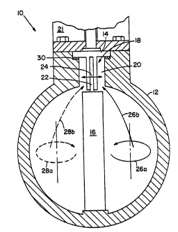
Refesring now to Fig. 1: the present invention
includes a vortez shedding meter 10. which primarily
consists of s metes body 12, a piezoelectric seasor
14, sad a shedder body 16. The piezoelectric vortez
sensor 14 eztends through a cylindrical opening 18
of meter body l2 and s~ainst vortez shedder 16.
Beasor ll is secured in place by a cap 21 bolted to
~aeter body 12. This construction permits sensor 1!
to be easily replaced, if it becomes damaged.
Sensor 1! divides a fluid cavity 20, defined by
opening 18. into two halves. A gasket 22, which is
psefessbly made of suitable high-temperature
material, creates a seal between the walls of fluid
w~9,i~o»a . Pcrius9oio~ass
~~a~~l~
cavity 20 and shedder 16.
. The sensor is oriented such that its sensing
direction is perpendicular to shedder 16 (as
indicated by a double headed arrow 24) and along the
direction of fluid flowing and through meter body 12
(for ezample into the pipe). This orientation
permits sensor 14 to detect the alternating pressure
signals 26b and 28b caused by vortices 26a and 28a.
As suggested by solid arrows 26a and 26b and the
dashed arrows 28a and 28b, the pressure signals are
alternately transferred to each half of fluid cavity
and are 180 degrees out of phase with each
other. A second gaakct 30, preferably made of
high-temperature material, is secured between sensor
15 14 and meter body 12 to prevent ezternai leakage of
f laid.
A more detailed~drawing of sensor 14 is shown in
Figs. 2 and 3. 6ensor 14 includes a sensor housing
32 and a spool-like actuator 34 which shuttles back
20 and forth, as indicated by arrow 36. in response to
alternating vortices. Hoth sensor housing 32 and
actuator 34 are constructed from high temperature.
low corrosive materials, such as stainless steel.
The active parts of sensor 14 are contained by
sensor housing 32 and are designed to have a low
mass. The importance of designing the active parts
so that they have a low mass will be discussed in
greater detail below.
In the preferred embodiment. sensor housing 32
is fabricated by boring cylindrical bores 38 (Fig.
3). which are spprozimately 1.3 centimeters in
diameter, on each side of sensor housing 32 leaving
a center member 40 having a channel 42. Two
cavities 44 and 46, each approzimately 2 millimeters
WO 91/10114 PCT/US90/07485
:,
2~~fl~~l~
- 8 -
deep, are thereby formed. Actuator 34, which '
primarily consists of an azie 52 and flanges 54 and
56 connected at each end of azie 52, is positioned
within bores 38 and held in place by diaphragms 48
and 50 (Fig. 2). J~le 52 is sized to be alideably
disposed within channel 42 to permit flanges 54 and
56, to shuttle back and forth within cavities 44 and
46. Flanges 54 and 56 are approzimately 11
millimeters in diameter and 2 millimeters thick.
Diaphragms 48 and 50, approzimately ?5 micrometers
thick and are sufficiently flezibhe to allow
actuator 34 to shuttle back and forth in response to
vortez pressure. The diaphragms hermetically seal
each cavity 44 and 46 from the flow of fluid in
meter body 12.
Sandwiched between each flange 54, 56 and center
member 40 is a piezoelectsic sensing element 62, 64
and biasing mechanism 58, 60. Sensing elements 62
and 64 are preferably lithium niobate piezoelectric
crystals, which are Z cut. The advantages of using
a lithium niobate piezoelectric crystal over other
types of crystals is its ability to remain
piezoelectrically active while continuously
opesating at high temperatures such as 800 degrees F
(Their Cusie temperature is 2102 degrees F.).
According to.the preferred embodiment, both crystal
polarities are facing the same direction. In other
words. the positive face of one crystal and the
negative face of the other crystal are in contact
with center member 40 which serves as both an
electrical and mechanical ground. When assembled in
this manner, both crystals produce the acme polarity
signal for a flow signal which shuttles actuator 34
back and forth as indicated by arrows ?4 and ~6.
0
V1'O 91/10114 PCT/iJS90/01485
~~3~~a'~~~
_ g
' Thia will be discussed in greater detail below.
Hissing mechanisms 58 sad 60 preferably consist
' of Hellavfile washers 66 and 68 made of suitable
spring alloy for high temperatures and insulating
disks 70 and 92, preferably made of ceramic. Bias
mechanisms 58 and 60 serve to uniformly apply
compressive force on each sensing element 62 and 64
to keep all of the pieces of the sensing mechanism
in intimate contact with each other. Other suitable
biasing means can also be used. For ezample, a
helical spring may be used in place of the
Helleville washer.
Crystals 62 and 64 are placed in sensor housing
32 with one face in electrical contact with center
member 40 which serves as both the electrical and
mechanical ground for the sensor mechanism. Sensing
circuitry 98 is connected to the crystals via leads
80 and 82 which are connected to foil discs 84 and
86. Foil discs 84 and 86 are disposed between
insulators 90 and 92 and sensing crystals 62 and 64,
and are kept in contact with the crystals by bias
means 66 and 68. Foil disks 84 and 86 are
approzimstely ilmm in diameter and 50 micrometers
thick.
6enaing circuitry 98 is preferably located
remotely from sensor body 14 to protect it from
eztreme temperatures. As shown, electrical leads 80
and 82 are rigidly supported by a dual bore ceramic
tube 88. Ceramic tube 88 is encased by a staialess
steal eztension tube 90 which is welded leak tight
to sensor housing 32. Leads 80 and 82 can be brazed
or welded to a ceramic to metal electrical
feedthrough (not shown) welded leakti9ht to the
eztenaion tube. This allows the sensor to be
WO 91 /10114 PCT/US90/07485
~~~~~1~
- to -
evacuated and filled with a dry gas for preventing
degradation of the sensor.
During operation of the meter, vortices generated
by shedder 15 apply an alternating differential
pressure across the two aides of the sensor 14. As
a result, actuator 34 shuttles back and forth (as
indicated by arrow 36) causing one Belleville washer
to further comgress slightly while simultaneously
relating the other slightly. This in turn creates
an increasing stress on one crystal while
simultaneously decreasing the stress on the other.
These alternating stress variations cause
alternating charges to be generated at the faces of
each crystal which are measured by sensing circuitry
'18.
An important feature of this sensor construction
is that it is insensitive to line pressure
fluctuations such as those commonly caused by pump
impeller rotation. These pressure fluctuations
travel down the pipe at sonic velocities and arrive
at both sides of the sensor simultaneously sad are
referred to as common mode noise. These pressure
fluctuations can be substantially greater than the
alternating differential pressure signals created by
vortez shedding, particularly at low flow rates. If
the sensor were affected by common mode pressure
fluctuations, an erroneous readout could result.
Since the two diaphragms 48 and 50 have essentially
the same effective area and are coupled to each
other via spool-like actuator 34, pressure
fluctuations which arrive simultaneously at both
sides of sensor 14 create no net force on crystals
62 and 64. In other Words, equal and opposite
forces are generated and no motion of the shuttle
WO 91/10114 PCT/US90/074$5
..--,,
2~~~~~~
- 11 -
occurs. As a result, no differential stresses are
transferred to the crystals
and no charges are generated by either crystal.
Common mode signals could also cause very alight
and simultaneous bending of both spool flanges 54
and 56, resulting in a simultaneous increase (or
decrease) in stress on both crystals. Since the
stress on both crystals is changing in phase
(whereas the stresses created by vortices 26 and 28
are changing 180 degrees out of phase) the resulting
signal can be electronically cancelled.
A sensor constructed in this manner is also
inherently insensitive to mechanical vibrations.
Lateral pipe vibrations (vibration that is parallel
to the shuttle direction of the sensor) are not an
important factor because the sensor has a very small
active mass (spprosimately 2 grams). For ezample, a
"1 g" vibration produces a 2-grams lateral force,
which is less than the force produced by vortex
shedding at flow ranges of interest. The sensor is
insensitive to vibrations either along the flow
direction or in the vertical direction because in
addition to the very small sensor mass, these
vibrations create shear stress on the crystals and
crYstais polarized through their thickness are
insensitive to shear stress.
Signals can be generated, however, by both
crystals when a common mode pressure signal, such as
that arising from pulsating flow, is applied to the
sensor. These signals can occur only if the
mechanical characteristics of the sensor are less
than ideal. The mechanical response can be of two
forms. First. due to the lack of symmetry of a
sensor, the crystals can be compressed or relaxed
V1!~ 91 /10114 PC1'/US90/07485
2t~~~~l.~
- 12 -
unequally. For ezample, one of the diaphragms may
be more flezible or have a larger surface area than
the other and may therefore be more sensitive to
pressure variations. These types of symmetry
variations result in differential pressures that are
similar to forces arising in the vortez field when
flow is present. These signals can not be
distinguished from the flow signal. Therefore,
symmetry is an important consideration during the
manufacture of the sensor.
The second type of mechanical response that can
occur is due to the non-rigidity of actuator 34
which could cause compression on both crystals to be
increased or relazed simultaneously. In other
words, each flange. 54 and 56 could bend or the azei
could be compressed under pressure. Electronically,
this type of response can be distinguished and
eliminated from the signals generated by shedding
vortices because the two crystals will produce small
signals of opposite polarity. The preferred
circuitry for eliminating these signals is discussed
in greater detail below.
The preferred cireuitry 78 for detecting
vortices is shown in Fig. 4. This circuitry shows a
circuit 92 which is an electrical equivalent of the
crystals and a charge amplifier 93. As shown, this
approach requires that the two piezoelectric
crystals be mounted so that the polarities of the
two crystals in contact with center member 40 are
opposite, as discussed above. This insures that
when both crystals are simultaneously compressed or
relased the charge developed across the crystals, as
detected by electrodes 80 and 82, will be equal in
magnitude (if the crystal's are identical and the
WO 91/10114 PCT/US90/07485
P
~r~~~l~
- 13 -
meehanical components symmetric), but opposite in
sign.
Circuit 92 includes crystal capacitors 94a and
94b and crystal resistance 96a and 96b connected in
series with voltage sources 98a and 98b for each
. crystal. Charge amplifier 93 includes an
operational amplifier 102 having a negative terminal
104 interconnected to a node 105 between crystal
resistances 96a. 96b and capacitors 94a, 94b. A
positive terminal 106 of operational amplifier 102
is interconnected to a node 107 between crystal
capacitor 94a, 94b and resistors 96a. 96b and tied
to ground. Two diodes 108 and 110 are connected
between terminals 104 and 106, as shown to limit the
magnitude of the signals reaching the input
terminals of amplifier 102. Charge amplifier 93
also includes a feedback loop, which includes a
feedback capacitor 114 and a feedback resistor 116.
Since operational amplifiers characteristically
have a small do potential of its input, referred to
as its zero offset voltage. operational amplifier
102 will attempt to force a constant current to flow
through feedback capacitor 114. .If a constant
current were allowed to flow through feedback
capacitor 114, the voltage across it would increase
linearly With time. Eventually, this voltage will
cause the autput of the operational amplifier to
saturate. This condition is avoided by feedback
' resistor 116. which is placed in parallel with
30feedback capacitor 114. This resistor provides an
alteznative path for this constant current. As a
result. the voltage across the feedback loop is a
small fined value which is independent of time. A
resistor 109 and a capacitor 112 are connected in
WO 91/10114 PCT/U590107485
- 14 -
series between node 105 and negative terminal 104 to '
limit the gain of the circuit at high and low
frequency.
The charge amplifier is necessary to detect
electrical responses from the lithium niobate
crystals because characteristically they have very
low capacitance. For a:ample, these crystals have a
dielectric constant of approximately 30, as compared
to P2T5A piezoelectric crystals, which have a
dielectric constant at room temperature of
approximately 1800. Further, tests have indicated
that the resistance of these type of crystals drops
off sharply as temperature increases. Therefore,
using a voltage amplifier would be impractical. At
very high frequencies and low temperatures the full
crystal voltage would appear across the amplifier.
At low frequencies, and/or high temperatures, most
of the crystal voltage would appear across its
capacitor and not across the input to the voltage
amplifier.
Charge amplifier 93 operates by maintaining
negative terminal 104 of operational amplifier 102
at a potential close to ground. As a result, there
is essentially no potential difference across
crystal resistors 96a and 96b. The charge that
.appears across the crystals due to an applied stress
is nullified by charge flowing from the feedback
capacitance 114 to force the potential at negative
terminal 104 close to virtual ground.
When differential pressure generated by
alternating vortices forces the actuator to shuttle.
to one side of the sensor housing, increasing stress
on one crystal while relaxing the stress on the
other crystal, a positive or negative net charge
WO 91 /10114 PCl /US90/07485
2~~~15
-15-
develops at node 105. Charge amplifier 93 senses
this net charge and cancels it by delivering an
equal and opposite charge to the crystals. ors a
result, operational amplifier 102 generates an
output voltage ~VOUt) that is proportional to the
net charge across the crystals. The frequency of
this voltage signal is then measured to indicate the
frequency of the vortices.
Ideally, signals generated by the two crystals
as a result of a common mode pressure signal are
completely eliminated, if the mechanical and
electrical components are symmetric, by simple
subtraction or cancellation at node 105. For an
asymmetrical sensor, the net common mode signal at
node 105 is significantly reduced.
In the event the rigidity of the actuator is not
sufficiently high, and if, in~addition asymmetries
in the mechanical and electrical components of the
sensor a:ist, the electrical responses from the two
crystals in the presence of a common mode pressure
signal may not be sufficiently equal in magnitude to
allow for elimination by cancellation as outlined
above. As shown in Fig 5, this problem can be
solved by employing two charge amplifiers 120 and
122, one for each crystal. pots that cbarQe
amplifiers~120 aaa 122 are essentially equivalent to
charge amplifier 93. as shown in Fig. 1, and that
the crystals are mounted in a similar manner as
described shove, i.e. the polarities of the two
30crystsls with respect to center member 40 are
opposite. The common mode noise resulting from
these asymmetries is eliminated by adjusting the
relative value of the amplifier outputs, using an
adjustable resistor 126 of a summing circuit 7,24, to
~1(~ 91/10114 PCf/US90/07485
2~~~~1~
- 16 -
equalize the output signals of charge amplifiers 120 '
and 122 prior to cancellation at node 108. Summing
circuit 124, which includes an amplifier 132, is a '
common circuit known to one skilled in the art.
In the above implementations (Fig. 5), the
sensor could be assembled with common polarities of
' the two crystals in contact with center member 40 as
shown in Fig. 6. This circuit would then require an
inverter 130 to invert the signal generated by one
of the crystals before summing the signals together
as described above.
While this invention has been particularly shown
and described with reference to preferred
embodiments thereof, it will be understood by those
skilled in the art that various changes in form and
details may be made without departing from the
spirit and scope of the invention as defined in the
appended claims. For esampie. other piezoelectric
crystal such as tantalite or quartz crystals. or
piezoelectric ceramics are sensing elements which
may be used depending on the application. For these
crystals the use of a voltage amplifier circuit may
be desirable to detect signals generated by the
crystals. Further, it will be understood by one
skilled in the art that the shuttle design of the
sensor could be fabricated with only one
piezoelectric element. Due to asymmetries in the
sensor, however, the common mode rejection ratio
would not be as great as with two elements as
described in the preferred embodiment.