Note: Descriptions are shown in the official language in which they were submitted.
20~1 112
ANAT.OGU33 MEMORY DEVICE
The present invention relates t:o novel analogue
memory devices capable of being set and reset to a
plurality of different conductance states.
Most semiconductor devices are used in binary
digital systems in which the device is in one of two states
(e.g. a high and low resistance) which can be used to
present binary 0 and binary 1. Howevex there is increasing
interest in devices which can be in more than two states.
Devices which can be set and reset into more than two
conductance states (as opposed to the two states of digital
devices) are potentially useful in structures known as
neural networks which attempt to reproduce some of the
arrangements of the human brain.
According to the present invention there is
provided an analogue memory device capable of being set and
reset into a resistance which is a measure of a voltage
applied to it, and which device comprises~
(a) a first conducting layer;
(b) a single thin layer in direct electrical contact with
layer (a);
(c) a metal top contact in electrical contact with layer
(b), the metal being one of V, Co, Ni, Pd! Fe or Mn;
wherein layer (b) constitutes said resistance and it is
located between layer (a) and layer (c), said layer (b)
being formed of pure or doped amorphous silicon; pure or
doped amorphous hydrogenated silicon or a hydrogenated
silicon alloy and wherein layer (b~ had been subjected to
a voltage sufficiently high to convert it into an analogue
.,. . ~ .
memory device. -~
The nature of the first conducting layer is not
critical as long as it is possible to grow the required
, . ... . .
amoxphous silicon (a-Si) layer upon it. Examples of ~ -
suitable materials are Cr or V. Examples of unsuitable
: ~ --
,. .. ,:
~b
; "..':.:
~:: . - : ,,
20~12
materials are gold (which diffuses into the a-Si layer and
mercury (which is liquid). The first conducting layer need
not extend on the whole area of the amorphous silicon
overlying it. Reference to the amorphous silicon layer
being above the first conducting layer do not carry any
implication about the orientation of the device in use but
are intended to indicate only that the silicon is deposited
after the first conducting layer.
The amorphous silicon must be dopable i.e. it
must be possible to increase its conductivity by
incorporating elements having higher or lower valency than
silicon. Some techniques of depositing amorphous silicon
may give silicon containing high levels of defects which
cannot be doped e.g. Argon sputtering of a Si target in the
absence of hydrogen. However methods of making dopable
amorphous silicon are well known to those skilled in the
art. Thus low pressure pIasma decomposition of silanes
(optionally in the presence of hydrogen or fluorine on to
a heated substrate may be used).
The deposition of amorphous silicon is discussed
in W. E. Spear and P. G. LeComber, Topics in Applied
Physics, Vol 55, (The-Physics of Hydrogenated Amorphous
Silicon I) 1934 pages 65-71.
The amorphous silicon is doped. The silicon may
be doped to produce n-type conductivity by incorporating an
element with a higher valency e.g. P, or may be doped to
give p-type conductivity as a result of introducing element
of lower valency e.g. B.
The amorphous silicon is, preferably, doped so as
to have a conductivity in the bulk state of at least 10-6
(ohms cm)-1. The degxee of doping is more preferably such
as to correspond to p' or n~-silicon e.g. to conductivities
greater than 10-4 (oh~s cm) 1.
:
.:~ , ,
::
B
2 ~ 2
-- 3
Methods of producing doped amorphous silicon are
well known to those skilled in the art. The silicon is
preferably p~ silicon.
The thickness of the doped amorphous silicon is
5preferably in the range 200 Angstrom to 0.35 micrometres
(20 to 350 nm). The amorphous silicon ]Layer may be pure
hydrogenated amorphous silicon (apart from any doping) or
may be a hydrogenated silicon alloy, e.g. a silicon
germanium alloy.
10The dopable silicon or silicon alloy may contain
fluorine.
The identity of the top contact is important in
obtaining analogue memory properties. In the production of
semiconductor devices semiconductor layer~ are often
15deposited on a conducting substrate and a metal layer is
deposited in a final step after the semiconductor layers
have been deposited. This metal layer is the top contact
of the device. The metal layer may, of course, be covered
by encapsulating layers or by an additional metal layer
20which is used to obtain better contact with the metal layer
in direct contact with the silicon. It is common in the
semiconductor industry to stack devices one above the other
in integrated circuits. It may be possible to stack other
semiconducting and conducting layers above the device of
25the present invention to form other devices within a single
integrated circuit.
Preferably the top contact metal is V, Co, Ni or
Pd.
The metal may be deposited for example by thermal
30evaporation or by sputtering.
The thickness of the metal is not believed to be
critical. Those skilled in the art will understand that
the normal requirements for producing metal contacts will
imply certain limits~ Thus there may be problems of
:.- .: . . ,
''' " "''': .
~- :
2 ~ 2
electrical continuity if the layer is too thin and there
may be problems of mechanical strain if the layer is too
thick. The thickness of the layer may for example be 50
Angstrom (5 nm) to 50 micrometres, pre~erably lO0 Angstroms
(10 nm) to l micrometre, more preferably 20 nm to 50 nm.
The device is a two terminal device. It is
preferably in the form of a layer of amorphous silicon of
a single conductivity type deposited on a conductive
substrate as bottom contact. The nature of the bottom
contact is not believed to be critical. Thus the bottom
contact may be Cr even though Cr does not give usePul
analogue memory properties when used as a top contact.
The top contact is preferably in contact only
with a relatively small area oP the amorphous silicon layer
for each device, as this allows large numbers of devices to
be fabricated in a small area, so giving compact integrated
circuits. A typical contact has an area of 10-6 cm2. This
can be readily achieved by the well-known process of
photolithography.
A step of applying a voltage across the device to ~ -
change the electrical characteristics is re~uired~ Such -
permanent electrical modification of semiconductor devices ~ -
is often known as "forming" to those skilled in the art. -~ -
The device as initially produced, before being subjected to
the "forming" step has a relatively high resistance. Thus
the resistance may be of the order of 109 ohms.
For the prePerred device containing only silicon
of a single conductivity type reference to Porward on
backward bias are meaningless and in principle it does not
matter whether the top contact is positive or negative in
relation to the bottom contact during the forming process.
Preferably, however, the top contact is positive
in relation to the bottom contact during the forming
process.
-
; ' ,
; : .
2 ~ 2
The forming step is preferably divided into two
stages, a "soft" forming step and a "hard" ~orming step.
The "hard" forming step is a step which converts the a-Si
structure into a device having the desired analogue memory
properties. It is possible to "hard" form the device in a
single step by applying a voltage which is sufficiently
large to convert the structure to a memory device having a
resistance less than the full OFF state. However, as
indicated above, it is preferred to carry out a "soft"
forming step initially. This involves applying a voltage
which is sufficiently high (for example 13-14 volts3 to
permanently change the characteristics of the device and to
reduce its resistance (for example, by two orders of
magnitude) without transforming it to a device having
analogue mPmory properties. The final "hard" forming step
may be carried out by applying a further, slightly higher
voltage (for example the order of 1 to 2 volts above the
soft-forming voltage). Thus the initial "soft" forming
events can be used to judge the voltage required for hard
forming, resulting in a more controlled process. After
"hard" forming the resistance of the analogue memory device
will be lower than that of the "so~t" formed structure ~for
example an order of magnitude or more lower). It will then
be below the maximum resistance (the fully OFF stage) to
which it can be reset in use.
The magnitude of the forming voltage depends on
the thickness of the amorphous silicon layer. It is
preferably in the range 6 to 16 volts.
It is necessary to control the energy applied to
the structure, as excessive energy can produce damage which
prevents a satisfactory device being produced. The energy
; can be controlled by placing a resistance in circuit and by
using short voltage pulses. Example of pulse lengths which
may be used are 50 ns to ~ microsecond.
:
~ ~ . "'
~ .
2~1112
-- 6
The devices of the present invention can be set
and xeset to a resistance which is a measure of an applied
voltage. By "set" we mean that the device will retain this
resistance even when the voltage which caused it to take
this resistance has been removed. By "reset" we mean that
the resistance can be changad to a new set value and is not
permanently fixed in the original set value. The devices
of the present invention are thus distinguished from
threshold devices which only retain a given stage as long
as a holding voltage is applied to them. They are
different fr~m the known binary memory devices in which the
resistance may depend on the applied voltage but all
voltages below a certain value correspond to one resistance
and all voltages above another value correspond to another
resistance. The devices of the present invention do not
show analogue memory properties over the whole range of
voltages which can be applied to them. It will bP
appreciated that a device which shows analogue memory
properties over a voltage rang~ of say 10 millivolts is not
in practice a useful device. It is preferred therefore to
select metal contacts which give analogue memory properties
over a voltage range of at least 0O5V, and preferably over
at least one V, more preferably over more than 2V.
The device after "forming" will normally be in a
resistance state between the ON and OFF states. By
applying a positive voltage pulse of sufficient voltage to
the top contact, the device can be set into its highest (or
OFF) resistance state. It can then be placed in a lower
resistance state by making the bottom contact positive with
respect to the top contact. If the voltage is sufficiently
high the devicP will be switched to its minimum resistance
(the fully ON state). Lesser voltages, providing they are
within the appropriate voltage range will switch the device
-. -
~ B
~ .
2~112
- 7 -
to an intermediate resistance which is related to the
voltage applied.
An alternative method of setting the device is to
apply a sufficient voltage to switch the "formed" device
back to the fully ON state. It may then be switched to a
lower resistance intermediate between the fully OFF and the
full ON states, by the application of a positive voltage to
the top contact.
The switching in the "formed" analogue memory
device is preferably carried out with short voltage pulses
for example pulses of length in the range 10 ns to 500
nsec. -~
The invention will now be described with
reference to the accompanying drawings in which:
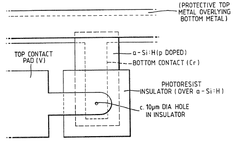
Figure 1 is a plan view (not to scale) of a
memory element in accordance with the present invention;
Figure 2 is a diagrammatic representation of a -
circuit used in testing a memory element made in accordance
with the invention;
Figure 3 is a graphical representation of the
change in resistance during the forming process: -
Figures 4 and 5 are graphical representation of
the change in resistance of a formed device with changing
ERASE voltage;
Figures 6 and 7 are graphical representations of
the variation of resistance with number of constant voltage
ERASE and WRITE pulses applied to a device according to the
invention, the constant ERASE pulse being of a greater
magnitude in Figure 7 than in Figure 6; :
30 ~ Figure 8 is a graphical representation of the
change in resistance of a device according to the invention -
as WRITE Pulses of increasing magnitude are applied to it,
Figure 9 is a graphical representation of the
change in resistance of a device according to the invention
' . :,
, ': ': .
2 ~ 1 2
alternatively subjected to an ERASE pulse of constant
magnitude and a WRITE Pulse of increasing magnitude;
Figure 10 is a graphical representation of the
change in resistance of a device according to the invention
initially in its ON stage and subjected to ERASE pulses of
increasing magnitude;
Figure 11 is a graphical representation of the
change in re istance of a device according to the invention
which is initially in its ON stage and which is
alternatively subjected to ERASE pulses of varying
magnitude and WRITE Pulses of constant magnitude;
Figure 12 is a graphical representation of the
change in resistance of a device according to the invention
which is initially in the OFF state and which is subjected
to WRITE Pulses which increase in magnitude;
Figure 13 is a graphical representation of the
change in resistance of a device according to the invention
subjected to alternatively WRITE and ~RASE Pulsest with the
ERASE Pulse held constant and the WRITE Pulse increasing in
magnitude;
Figure 14 is a graphical representation of the
change in resistance of a device not according to the
present invention which is initially in a high resistance
state and which is subjected to voltage pulses of
increasing magnitude, showing the rapid transition from a
very high resistance state to a high resistance staLe when
a critical voltage threshold is exceeded;
Figure 15 is a graphical representation of the
~; change in resistance of a device not according to the
invention which is initially in an ON state and is
subjected to ERASE voltage pulses o~ increasing magnitude;
and
Figure 16 is a graphical representation of the
change in resistance of a device not according to the
::
.:
2051~12
g
invention which is initially in the OFF state and which is
subjected to WRITE Pulses of increasing magnitude.
It should be noted that in a digital device a
WRITE pulse can be considered as one which sets the device
to a state corresponding to either binary 0 or I while an
ERASE pulse can be considered as a pulse whish always
resets the device to a~ oppo ite state (binary 1 or 0). In
the present specification a WRITE pulse is a pulse which
tends to reduce the resistance of the devic~ and an ERASE
pulse is a pulse which tends to increase it. Thus a STORE
Pulse which stores analogue information in the device about
the magnitude of the voltage applied to it may be a WRITE
or an ERASE pulse. A RESET Pulse which turns the device
fully ON or OFF may thus be a WRITE or ERASE pulse provided
it is of sufficient magnitude to change the device to the
fully ON or OFF state. -
Example 1
A structure comprising a glass substrate,
chromium ~irst conducting layer, a layer of hydrogenated
amorphous silicon doped with diborane, (B2H6), 1 and a top
contact layer was fabricated as follows: ~ -
The glass structure was "Corning 7059" glass
("Corning" is a trade mark) of thickness about 0.75 mm and
length and width 45 mm and 20 mm respectively. A chromium
layer of thickness about 150 nm was deposited on this
substrate by standard thermal evaporation of chromium
granules from an electrically heated tungsten ~ilament in
vacuum and subsequently patterned by conventional
photolithography.
The amorphous silicon was deposited on this
substrate in a single layer by the radio frequency glow
discharge decomposition o~ a mixture of SiH4 and about 104
ppm of B2H6, obtained by admitting silane gas and a gas
mlxture of 5% diborane in hydrogen to the vacuum system via -~
., .,.: .'
2~1112
flow controllers. The glass substrate was mounted on a
substrate holder contained within a vacuum pumped glass
tube enclosure and heated to 310C (via a heater element
contained within the substrate holder) at a vacuum of less
than 10-6 torr. Nitrogen gas was then admitted to the
system to raiss th~ vacuum to 0.1 torr and a gas plasma
discharge induced (as defined below~ Eor a period of 4
minutes (power input 8~). The discharge was then
extinguished, the Nz flow stopped and the system pumped
below 10-6 torr. The silane/diborane/hydrogen gases were
then admitted to the chamber, flow conditions being set to
achieve both silane/diborane ratio and a constant gas
pressure of 0.1 torr, resulting from the balance of
incoming gas flow and outgoing pumped gas. A gas plasma
discharge was then induced using a radio frequency
generator running at 40MHz and capacitively coupled to the
gas via the substrate holder and two external secondary
electrodes 6cm away from the substrate. Power input from -
the generator was 8 watts corresponding to a power density
of 2OmW/cm2 at the substrate. The RF discharge was -~
maintained for 5.5 minutes and then extinguished. The
resulting sample was cooled under vacuum and removed from
the deposition system. The a-Si film resulting from this
was measured to be 900 Angstrom thick +50 Angstrom (90 nm
~5 nm). The level o~ conductivity due to the B2H6 doping was
measured to be between lo-3 and 10-2 (ohms.cm)-1 in separate
experiments using the same deposition conditions,
corresponding to pta-Si H. -
The amorphous silicon layer was then patterned
using conventional lithography into a number o~ discrete
elements o~ dimensions 900 x 500 micrometres, overlying
regions of the chromium first conducting layer. An
insulator layer was then provided over all but a very small
area of the amorphous silicon, (itself overlying the first
:: :
~05~112
11 --
conducting layer), in order to define the area to be
contacted by the final metal. This was done using a 1.2
micrometres thick insulator of photoresist (Shipley
~` Microposit Sl818) which was patterned, baked and cured at
200DC to d~lineate the device area of Io-6 cm2.
A top contact of vanadium was deposited over the
device by the thermal evaporation of vanadium foil from an
electrically heated tungsten filament in vacuum, to a -
thickness of 60 nm. This was patterned using conventional
lithography techniques to provide individual contacts to
each of the previously defined a-Si elements; this
patterning also provided probing pads of the vanadium to -~
one side of the devices, isolated from both chromium first
layer and the a-Si layer except in the previously-defined
contact area. Figure 1 shows a plan view of the device
made by this technique. -
The finished sample was designated 779/l. The
electrical characteristics of an individual element on this
sample were measured as follows.
2Q The element was contacted using two electrical
probe needles contacting the top and bottom metallisations.
These probes were connected to a switching network, such
that with the switch in either one of two positions one
probe was connected to the pulse generator and the other
probe was connected to one side of a resistor (Rs) and the
input to an oscilloscope, the other side of the resistor
being connected to earth. With the switch in the opposite
position, these connections were reversed. The circuit is
shown in Figure 2. Hence, application of a voltage pulse
to the device, using the pulse generator, induced a current
in both the device and resistor ~, thereby inducing a
voltage proportional to this current at the oscilloscope
~;; input. Measurement o~ this voltage allowed calculation of -
~ the device resistance. It will be appreciated that the
1: ;~` ~ . -
'~ r.~
2~1112
- 12 -
value of Rs needs to be sufficiently low to permit most of
the applied voltage to appear across the device, yet large
enough to give a detectable signal on the oscilloscope.
Typically, Rs values of from 1 M ohms (for forming and
initial informed measurement) and 100 ohms (for switching
measurement) were used.
In order t~ measure device resistance, a low
voltage of 0.5V was output from the pulse generator as
continuous DC level; pulses for forming and switching were
superimposed on this. Initially, the resistance Q~ the
element as made above was measured to be greater than 108
ohms. The element was then subjected to a procedure in
which its electrical properties were modified by the
application of voltage pulses. A succession oP 250 nsec.
voltage pulses of progressively increasing voltage were
applied across the a-Si film, with top (V) contact being at
positive potential with respect to the first (Cr) contact.
After each pulse the element resistance was determined as
described above. Figure 3 curve~ 1 shows the device
resistant against previous voltage pulse as successive
pulses are applied. (Note that the device resistance is
stable until a further voltage pulse is applied and never `-
returns to its original value once modified). At a voltage -
of between 13.5 and 14 volts, the resistance fell abruptly
to a value of 7 x 10⁵ ohms, within the expected switching
range of this element. It was then possible to obtain an
even lower resistance in the device using far smaller
negative voltage pulses (3.4 V, 100 nsec), testifyiny to
the permanent and dramatic change in device properties of
the formed element were then studied.
Example l(a)
A positive pulse (100 nsec, 3.4 V) was first
applied to the element first contact (cr), resulting in an
ON state of 2x10³ ohms; (this is d~fined as a WRITE pulse).
. ; .
: -. '
t ~ c
2~51112
- 13 -
An opposite polarity pulse, positive to the top contact
(V), (defined as an ERASE pulse), was then applied at
successively higher voltages and the element resistance
determined after each. The results of this test are shown
in Figure 4. It can be seen that at a threshold voltage of
about 1.6n V, the element resistance is gradually increased
with each successively higher voltage until, at about 3.0
V, a final resistance state of about 4xlO5 ohms is achieved.
It should be noted that all the states attained were
non-volatile and stablel i.e. in the absence of any attempt
to switch the element (e.g. with zero bias or when
disconnected), it retained the conductivity state it had
last been set to.
Example l(b)
In order to ~ully demonstrate the voltaye
programmability of the device an alternative method of use
was tested. In this positive, 100 nsec WRITE pulse of 3.4
V was applied to the element first or bottom contact (Cr)
to set the element to its low resistance state and the
resistance measured (2x10³ ohms); a positive, 100 nsec ERASE
Pulse of, initially 1.2 V was then applied to the element
top contact (V) and the device resistance remeasured. This
procedure was repeated with the ERASE pulse being increased
by 0.05 V on each successive occasion. The results of this
test are shown in Figure 5: as expected, the application of
the WRITE Pulse resulted in a constant resistance value
whilst increasing ERASE Pulse amplitude gave rise to a
range of resistance values between 2 x 10³ ohms and 4 x 10⁵
ohms. This demonstrates that, between the upper and lower
switching thresholds, the element resistance is primarily
a function of applied voltage pulse, not of the number of
pulses applied as might be deduced from Figure ~. Thus the
element can controllably be set on an intermediate
resistance between an upper and lower bound. The
2051~1 2
- 14 -
reproducibility of the switching to these intermediate
resistance states was tested by repeatedly applying fixed
ERASE and WRITE Pulses of 100 nsec, 3.4 V and ERASE Pulses
of loo nsec 2.1 V and 100 nsec 2.4 V are shown in Figures
6 and 7 respectively. Over the duration of the test, the
application of fixed pulses results in constant resistance
values. (The scatter in the value after ERASE is to be
expected due to small fluctuations in the value of applied
voltage from the equipment; it is because of its that a
wide voltage threshold range is desirable, in order to
provide as many usable intermediate states as possible.)
Example lfc)
A further method of using the element was teated.
The element was first set to its high resistivity state
(8xlO5 ohms) using an ERA5E pulse of ~3.4 V, 100 nsec
(applied to top contact ~V)). A series o~ WRITE Pulses of
100 nsec duration were then applied to the element,
starting at 1.2 V and incrementing each successive pulse of
0.05 V up to 3.3 V. The element resistance was ~easured ~-
a~ter each pulse and the results are shown in Figure 8. As
before, intermediate resistance states are obtained for
WRITE pulses between a lower threshold voltage and upper
threshold voltage (of ~bout 1.6 V and 2.7 V respectively), -
though there is far more scatter in the curve than for the
case of incremental ERASE (Figure 4).
~ ;
A further test was made in which a constant ERASE
pulse of 3.4 V, lOO nsec was applied to the element to
reset it to its highest resistance state, followed by a -
WRITE Pulse of lOO nsec, voltage being incremented by 0.05
V ~rom 1.2 V to 3.4 V on successive repeats. Resistance
was measured after each pulse and the results are shown in
Figure 9; as was ths case for constant WRITE, incremental
ERASE (Figure 5), the intermediate resistance states are
;~ ~ ''` . ''. :.
.
. .
~ .
-
2~1112
- 15 -
seen to be primarily a function of previously applied
voltage pulse.
Example ?
A sample was made as in Example 1, but with a
first metal layer of 50 nm vanadium deposited by thermal
evaporation as defined in Example 1. a-Si deposition was
done simultaneously with Example 1 and the finished sample
~V-p~-V) designated 779/2.
An element of this sample was tested as in
Example 1. Initially a series of 250 nsec positive voltage
pulses were applied to the top contact, each successive
pulse being of higher voltage than the last; element
resistance was measured after each pulse. The test was
stopped once the "forming" event was seen to take place
(i.e. an abrupt change in resistance to 6 x 10⁵ ohms). The
results of this test are shown in curve 2 in Figure 3.
A further 4 experiments (~a)-(d~ defined ion
Example 1) were then applied to the element to determine
the dependence of the element resistance on previously
applied voltage pulse.
Figure 10 shows the results of experiment (a),
(in which after initial WRITE Pulse (100 nsec, 3.4 V to
bottom contact), a sequence of 100 nsec ERASE pulses are
applied from 1.2 V to 3.2 V in 0.05 V steps)0
Figure 11 shows the results of an experiment (b)
(a sequence of alternating 3.4 V, lO0 nsec WRITE Pulses,
each followed by an incremented 100 nsec ERAS~ pulse from
experiment).
Figure 12 shows the results from experiment (c)
(initial ERASE pulse of 3.4 kV, 100 n~ec, followed by
incrementally increasing WRI~E pulses of 100 nsec, 1.2 V to
3.4 V in 0.05 V steps).
~; Figure 13 shows the result from experiment (d)
(alternative 3.4 V, 100 nsec ERASE Pulses followed by 100
~ ~ ~;p T
20511~2
- 16 -
nsec WRITE Pulses, incremented from 1.2 V to 3.4 V in 0.05
V steps).
These tests show that the V-p~-V sample behaves
similarly to the V-p'-Cr sample of Example 1; most
importantly, there is no indication that replacing the
first Cr metal layer with V induces further (opposite
polarity~ switching in the structure.
comparative Test A
A sample was made as in Example 1, but with a
final (top) metal layer of about 50 nm Cr, deposited as for
the first bottom metal layer. a-Si deposition was done
simultaneously with Example 1 and the finished sample
(Cr-p~-Cr) designated 779/3.
An element of this sample was tested as in
Example 1. Initially a series of 250 nsec positive voltage
pulses were applied to the top contact, each successive
pulse being higher than the last, until the "forming" event
took place. The results of this test are shown in Figure
14; note that resistance changes take place over a much
narrower voltage range than in the corresponding test on
Examples 1 and 2 (Figure 3).
After "forming", the element was tested using
method (a) and method (c) previously defined to determine
the presence of intermediate resistance states.
Figure 15 shows the results for method (a).
Figure 16 shows the results for method (c). Note
that although similar resistance limits are seen in this
element to those of Examples 1 and 2, (i.e. from 2 x 10³
ohms to 3.5 x 10⁵), and some intermediate states do exist,
- . .
the voltage range over which these intermediate states can
be obtained is far narrower than the range of Examples 1
and 2, (i.e. circa 0.15-0.2 kV compared with circa 2.2 V).
This makes it extremely difficult to obtain reliable
programming of the intermedlate states and the element lS
B
1 1 2
- 17 -
only suitable for digital use, (i.e. from the 2 x 10³ ohms
state to the 3.5 x 10⁵ ohms state), and is correspondingly
classified as a digital device.
Examples 3-8 and comparative Tests
A number of samples were made essentially as for
Example 1, (i.e. glass Cr first conducting layer, circa 900
Angstrom a-Si:H doped with H2H6), but a number of different
top contact metal films were deposited in place of the V
film of Example 1. Each sample was then tested as in ~ -
Example 1 and the range of switching voltages over which
intermediate states could be obtained was determined.
Devices were accordingly classified as digital ~switching
range 0.5 V) or analogue ~switching range 0.5 V); preferred
analogue devices were defined as those exhibiting a
switching range of 2.0 V or more. Table 1 lists the
results of this test. -
.:
B `::
2051~12
-- 18 --
TAaLE 1
Swvey of p+ -switching with different top metals
all the bottom contacts ars chromium.
T.E. = thormal evaporation of top metal.
S = sputterad top metal.
i_xampie Metal Switchlng Switching Comments
or top Method Type Range
test contact
B Cr T.E. Digital ~0.5 V Intermadiate
states oxist
3 v T.E. Analogue ~ 2.0V Preferrrd
2 0 4 Fe T.E. Analogue 0.5 - 1.0 V
Nl T.E. Analogue 2.0 V Preferred
C Au T.E. No swltchlng - -
D Cu T.E. No swltchln9 - - .; .
6 Co T.E. Analogue > 2.0V Prefsrred
3 0 E Ti T.E. Unstable ~ - ~
F Mo S Unstable - - .
7 Pd S Analogue 2.0 V Preferred
G W S Dlgltal
8 Mn - Analogua 0.5 -1.0 V
H Ag - Digital ~0.5V No
intermediate
states
obtalned
Ai - No swUching
.. -.
.
, - :