Note: Descriptions are shown in the official language in which they were submitted.
This invention relates to a control device that
controls a self-commutated inverter connected to an AC
(alternating-current) power system via a three-phase
transformer, and more particularly to an inverter
control device that suppresses DC (direct-current)
magnetization generated in three-phase transformer.
Large capacitance self-commutated inverters have
been used to regulate the reactive power of a power
system or to supply the DC power from fuel cells or
secondary batteries to a power system.
A typical voltage self-commutated inverter is com-
posed of an inverter main circuit~ which contains a
plurality of controllable rectifier elements and a
plurality of rectifier elements, a DC capacitor con-
nected across a DC side terminals of the inverter maincircuit, and a three-phase transformer having the
inverter side terminals connected to a AC side terminals
of the inverter main circuit on a phase basis and the
system terminals connected to the system on a phase
basis.
Such an inverter is able to control the three phase
output voltages of the inverter main circuit by changing
ON time of the individual controllable rectifier ele-
ments. The current exchanged with the AC power system
via the impedance of the three-phase transformer can be
controlled by regulating the phase and amplitude of the
three phase output voltages from the inverter main
~05~
-- 2 --
circult according to the phase and amplitude of the AC
system voltage.
Such inverter control is performed by an inverter
control device. Based on the active current reference
value and reactive current reference value, the inverter
control device determines an inverter output voltage
reference value that decides the three phase output
voltages of the inverter main circuit and then supplies
a gate signal corresponding to the inverter output
voltage reference value to the inverter main circuit to
control the ON time of each controllable rectiEier ele-
ment. This converts the DC power from the DC voltage
source connected to the DC side terminals of the
inverter main clrcuit into an effective power and sup-
plies it to the AC power system or regulates the reac-
tive power of the AC power system.
The above-mentioned inverter control device has the
following problem: a constant generation of a small
amount of DC component in the three phase output AC
voltages of the inverter main circuit creates a DC com-
ponent in the alternating magnetic flux in the three-
phase transformer, causing an excessive exciting current
to flow. That is, DC magnetization in the three-phase
transformer gives rise to overcurrent.
When DC magnetization in the three-phase trans-
former permits a current larger than the rated value to
flow in the windings of the three-phase transformer, the
~- 3 ~ 51~
transformer may burn out and an excessive current may
flow through the controllable rectifier elements consti-
tuting the inverter main circuit, which destroys the
elements, preventing the voltage self-commutated
inverter from functioning properly.
The reason why a small amount of DC component is
produced in the three phase output AC voltages of the
inverter main circuit is that slight differences in
characteristic between the controllable rectifier
elements making up the inverter main circuit lead to
differences in ON time between the controllable rec-
tifier elements on the positive and negative polarity
sides, creating a DC component in the output voltage.
The generation of a DC component in the inverter output
voltage reference value also causes DC components in the
three phase output AC voltages of the inverter main
circuit.
Although the problem of DC magnetization in the
transformer causing overcurrent can be overcome by pro-
viding a gap in the iron core of the transformer to makeit hard for magnetic saturation to take place in the
iron core, this approach is not desirable because of
larger size and higher cost.
The object of the present invention is to provide a
highly reliable inverter control device capable of pre-
venting not only the generation of overcurrent due to
DC magnetization in the three-phase transformer, but
- 4 - ~ ~ 5
also burnouts of the three-phase transformer and
controllable rectifier elements.
The foregoing object is accomplished by an inverter
control device comprising: an inverter control device
according to this invention, comprising: a current DC
component detecting circuit for detecting the current DC
components contained in at least two of the three phase
output AC currents of the inverter; a DC magnetization
suppressor signal generating circuit for producing two
correcting signals from the current DC components, the
two correcting signals being used to balance in amount
the three voltage DC components contained in the three
phase output AC voltages of the inverter respectively;
an output reference correcting circuit for correcting
two of first output references in accordance with the
two correcting signals and outputting three second
references including the two corrected values and one of
the first output reference; and a gate control circuit
for controlling the three phase output AC voltages of
the inverter according to the three second output
references.
With this arrangement, the voltage DC components
for two phases are regulated so that the imbalanc~d com-
ponents contained in the three phase output AC voltages
of the inverter may become zero between phases, which
causes the DC current component of each phase to be
zero, thereby suppressing DC magnetization.
- 5 _ ~ ~51~
This invention can be more fully understood from
the following detailed description when taken in con-
junction with the accompanying drawings, in which:
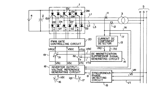
Fig. 1 is a functional block diagram for an
inverter control device according to an embodiment of
the present invention;
Fig. 2 is a circuit diagram for the current DC
component detector of the inverter control device in
Fig. 1;
Fig. 3 is a circuit diagram for the DC magnetiza-
tion suppressor signal calculating circuit of the inve-
rter control device in Fig. l;
Fig. 4 is an equivalent circuit diayram for
explaining a DC magnetization phenomenon in the trans-
former during inverter operation; and
Fig. 5 is an equivalent circuit diagram forexplaining how DC magneti~ation in the three-phase
transformer is suppressed.
Referring to the accompanying drawings, an embodi-
ment of the present invention will be explained.
Fig. 1 shows an overall arrangement of an embodi-
ment of the present invention.
A DC capacitor 2 is connected across the DC side
terminals of an inverter main circuit 1, the AC side
terminals of which are connected to a three-phase trans-
former 3 on a phase basis: R phase, S phase, and T
phase. Those inverter main circuit 1, DC capacitor 2,
~051~
-- 6
and three-phase transformer 3 constitute a voltage self-
commutated inverter. This inverter is connected to a DC
voltage source 4 via the DC side terminals of the
inverter main circuit l, while connected to a three-
phase power system 5 via the three-phase transformer 3.
The lnverter main circuit l is constructed by con-
necting controllable rectifier elements GU, GV, GW, GX,
GY, and GZ, and rectifier elements DU, DV, DW, DX, DY,
and DZ as shown in Fig. l. For the controllable
rectifier elements GU, GV, GW, GX, GY, and GZ, power
electronics elements with a self-extinguishing function,
such as GTOS ( Gate Turn Off transistors) or power tran-
sistors may be used.
An inverter control device is composed of Hall CT
circuits ll and 12, which detect the R-phase and T-phase
inverter output AC currents, respectively, a current DC
component detector 13, a DC magnetization suppressor
signal generating circuit 14, a synchronous phase
detecting circuit 15, which detects the system voltage
phase ~ of the system voltages VR, VS, and VT of the
three-phase AC system 5, an active current setting
unlt 16 to enter the active current reference value, a
reactive current setting unit 17 to enter the reactive
current reference value, an inverter output-voltage
reference generating circuit 18, an output reference
correcting circuit l9, and PWM gate controlling
circuit 20.
,,
2(:1 51~
The Hall CT circuits 1l and 12 are installed on the
R-phase and T-phase lines Ll and L3 among the conductor
wires L1 through L3 that connect the AC side terminals
of the inverter main circuit 1 with the inverter side
terminals of the three-phase transformer 3 on a phase
basls. The Hall CT circuit 11 detects a Hall voltage,
which is generated when the magnetic flux, caused by
the current flowing through the line Ll, penetrates
through the Hall element, and supplies the output as
an electrical signal. The Hall CT circuit 12 functions
the same way.
The current DC component detector 13 is constructed
as shown in Fig. 2, where reference character A indica-
tes an operational amplifier, R1 and R2 indicate
resistors, and C indicates a capacitor. Here, two
operational amplifier A, resistors Rl and R2, and
capacitors C make up two first-order time-lag circuits.
The current DC component detector 13 detects DC compo-
nents iRd and iTd from the inverter output AC currents
iR and iT supplied from the Hall CT circuits 11 and 12.
~ ased on the DC components iRd and iTd from the
current DC component detector 13, the DC magnetization
suppressor signal generating circuit 14, which is
constructed as shown in Fig. 3, obtains the inverter
output voltage correcting signals VRd and VTd that
balance the DC components in the three phase inverter
output AC currents, and supplies the signal VRd and VTd.
- 8 - ~05~;?~
The inverter output voltage reference generating
circuit 18 receives the inverter output AC currents iR
and iT, system voltage phase ~, active current reference
value idc, and reactive current reference value iqc.
The generating clrcuit 18, according to the active
current reference value idc and reactive current refer-
ence value iqc, produces the inverter output voltage
references VRC, VSC, and VTC as the first output refer-
ences that determines the three phase output voltages
of the inverter main circuit 1 so that the inverter out-
put AC currents iR and iT sensed at the Hall CT circuits
11 and CT 12 may be regulated.
The output reference correcting circuit 19, which
is composed of two adders 31 and 32 as shown in Fig. 1,
receives the inverter output voltage references VRC,
VSC, and VTC and the inverter output voltage correcting
signals VRd and VTd. The correcting circuit 19 corrects
the inverter output voltage references VRC and VTC on a
phase basis, according to the inverter output voltage
correcting signals VRd and VTd, and supplies the
corrected inverter output voltage references VRCC and
VTCC as the two of second output references. The
invérter output voltage reference VSC is supplied as the
corrected output reference VSCC as the one of the second
output reference without correction. The reason for
this will be explained later.
The PWM gate control circuit 20 compares the
- 9 - ~ O51~?J
corrected output references VRCC, vscc, and VTCC with a
triangular wave carrier signal and supplies gate signals
that det~rmine the ON time of each of the controllable
rectifier elements GU, GV, GW, GX, GY, and GZ consti-
tuting the inverter main circult l.
Referring to Figs. 4 and 5, how DC magnetlzation in
the three-phase transformer is suppressed will be ex-
plained in connection with the embodiment. Fig. 4 shows
a circuit for explaining a DC magnetization phenomenon
in the transformer during inverter operation, and Fig. 5
is a circuit for depicting the principle of suppressing
DC magnetization in the three-phase transformer.
For shortnessl sake, DC magnetization will be
described, referring to Fig. 4. It is known that
single-phase transformers have an equivalent circuit as
shown in Fig. 4, where reference character Zl indicates
the leakage impedance (the winding resistance plus the
leakage inductance) on the inverter main circuit side of
the transformer, Z2 indicates the leakage impedance on
the AC system side of the transformer, and Zm indicates
the magnetizing impedance (the iron loss plus the
magnetizing inductance) of the transformer.
If the DC voltage component of the output voltage
of the inverter main circuit is E and the AC system has
no impedance to the DC voltage component, then the
invert~r main circuit, transformer, and AC system will
form a circuit of Fig. 4 with respect to the DC voltage
- 10 - 2~51
component E. Thus, depending on the DC voltage com-
ponent E, DC currents il and i2 will flow. DC current
flowlng through the magnetizing inductance of the trans-
former causes DC magnetization. That is, the DC current
il causes DC magnetization. Since the magnetizlng
inductance is much larger than the leakage impedance, it
will take long time for the DC current il to become so
large that the magnetic flux in the transformer is
saturated to generated an AC overcurrent.
In Fig. 5, the impedances corresponding to the
inductances of the transformer and AC system are com-
blned into a single impedance for each phase: impedances
ZmR, zmS, and ZmT.
It is assumed that the DC voltage components for
the individual phases of the inverter main circuit are
ER, ES, and ET, respectively. To simplify an explana-
tion, the impedances ZmR, ZmS, and ZmT for the indivi-
dual phases are assumed to be the same value Z. In the
three-phase circuit of Fig. 5, if the following rela-
tions hold:
ER = ES = ET (1)then, the DC current components ilR, ilS, and ilT
flowing through the individual phases will be:
ilR = ilS = ilT = 0 (2)
That is, the differences between the DC voltage com-
ponents ER, ES, and ET for the individual phases allow
the DC current components ilR, ilS, and ilT to flow.
Derived from the three phase circuit conditions is the
next equation:
ilR + ilS + ilT = O (3)
Thus, if the DC current components for two phases among
three are detected, then the DC component for the
remaining phase will be determined. sased on these
equations:
ER - ES = Z * ~ilR - ilS)
= Z * (2ilR + ilT)
= (2*Z) * {ilR+(1/2)*ilT} (4)
ET - ES = Z * (ilT - ilS)
= Z * (2ilT + ilR)
= (2*Z) * ~ilT+(1/2)*ilR} (5)
if the DC voltage component ER iS controlled so as to
meet:
Z (2ilR + ilT) = O (6)
and the DC voltage component ET iS controlled so as to
meet:
Z (2ilT + ilR) = O (7)
then the relations (1) will hold. Thus, the relations
(2) will hold, so that even if each phase has a DC
voltage component, the DC current component flowing
through each phase becomes zero, which suppresses DC
magnetization. With this approach, DC magnetization is
suppressed by regulating only imbalanced components
without nullifying the DC voltage component for each
phase of the inverter main circuit, thereby making the
2~5~
- 12 -
control response of DC magnetlzation suppression faster.
In the embodiment, equations (4) and (5) are
calculated at the DC magnetization suppressor signal
generating circuit 14 constructed as shown in Fig. 3.
Reference character 21a and 21b indicate amplifiers that
multiply by a constant of 1/2 in equations (4) and (5),
22a and 22b adders that calculate the terms in braces
in equations (4) and (5), and 23a and 23b amplifiers
that calculate the term (2*Z) in equations (4) and (5).
Now, the operation of the embodiment constructed as
mentioned above will be explained.
Based on the active current reference value idc
from the active current setting unit 16 and the reactive
current reference value iqc from the reactive current
setting unit 17, the inverter output voltage reference
generating circuit 18 produces the inverter output
voltage references VRC, VSC, and VTC that determine the
three phase voltages of the inverter main circuit 1 so
that the inverter output AC currents iR and iT sensed at
the Hall CT circuits 11 an 12 may be regulated. In the
calculation of the inverter output voltage references
VRC, VSC, and VTC, the system voltage phase ~ sensed at
the synchronous phase detecting circuit lS is used to
determine the phases for the system voltages VR, VS, and
VT of the three-phase AC system 5.
The current DC component detector 13 receives the
inverter output AC currents iR and iT sensed at the Hall
- 13 - ~ ~5~
CT circuits 11 and 12, and detects the DC components iRd
and iTd contained in the inverter output AC currents iR
and iT.
In current transformers, which operate on the
same principle as the aforementioned transformers, DC
magnetization creatPs the same problem, so that the
signal containing a DC component cannot be sensed.
In the embodiment, however, use of Hall CT circuits
enables the signal containing AC and DC components to be
detected unlike current transformers.
In the current DC component detector 13, the cir-
cuits of Fig. 2 perform a first-order time-lag operation
on the inverter output AC currents iR and iT to detect
DC components iRd and iTd.
The DC magnetization suppressor signal generating
circuit 14 receives the DC components iRd and iTd of the
inverter output AC currents iR and iT and then produces
the right sides of equations (4) and (5) as the inverter
output voltage correcting signals VRd and VTd. In the
generating circuit 14 of Fig. 3, if the impedance Z
multiplied at the amplifiers 23a and 23b differs between
R and T phases, it must be adjusted for each phase.
The output reference correcting circuit 19 receives
the inverter output voltage references VRC, VSC, and VTC
from the inverter output voltage reference generating
circuit 18 and the inverter output voltage correcting
signals VRd and VTd from the DC magnetization suppressor
- 14 _ 205~
signal generating circuit 14. The correcting circuit 19
then subtracts the DC component VRd from the inverter
output voltage refèrence VRC to c~rrect the DC component
voltage ER in the R phase of the lnverter output voltage
on the right side of equation ~4) and supplies it as the
corrected output reference VRCC. The correcting circuit
l9 also subtracts the DC component VRd from the inverter
output voltage reference VTC to correct the DC component
voltage ET in the T phase of the inverter output voltage
on the right side of equation (5) and supplies it as
the corrected output reference VTCC.
In the embodiment, since the DC component voltage
ES in the S phase of the inverter output voltage is not
corrected, the inverter output voltage reference vSC is
supplied as the corrected reference VSCC.
The PWM gate controlling circuit 20 compares the
corrected output references vRCC, VSCC, and VTCC with a
triangular wave carrier signal and produces gate signals
that determine the ON time of the controllable rectifier
elements GU, GV, GW, GX, GY, and GZ constituting the
lnverter maln circuit 1.
For a detailed explanation of PWM gate control
uslng lnverter output voltage reference, an example is
disclosed in Shun-ichi Hirose, et al., "Application of
a digital instantaneous current control for static
induction thyristor converters in the utility line,"
PCIM Proceeding, pp. 343-349 Dec. 8, 1988 in Japan.
- 15 - 2~511~
The above-described current DC component detector
13, DC magnetization suppressor signal generating cir-
cuit 14, output reference correcting circuit 19, and PWM
gate controlling circuit 20 combine to control the DC
component of the inverter output voltage so that equa-
tions (6) and (7) may hold, which performs control so as
to fulfill equation (l). Consequently, the DC current
component in each of three phases becomes zero, thereby
suppressing DC magnetization.
Since in the embodiment of the present invention,
DC magnetization suppression of the three-phase trans-
former is performed by balancing the DC components of
the three phase output voltages of the inverter, making
use of the characteristics of the three-phase trans-
former, an increase in the DC magnetization suppressing
response speed of the three-phase transformer can reduce
the magnetizing current that saturates the iron core
flux in the three-phase transformer, which suppresses
overcurrent due to DC magnetization without using a
large-capacity three-phase transformer with a gap in the
iron core, thereby achieving a small inverter at low
cost.
In order to balance the DC components of the three
phase output voltages of the inverter, DC magnetization
is suppressed by detecting the current DC components of
two phases for the three phase output currents of the
inverter and correcting the inverter output voltages for
- 16 _ 2 ~ 5~ ~9
the two phase, which makes control easier, thereby
simplifying the inverter control device.
While in Fig. 1, the DC magnetization suppressor
signal generating circuit 14 and output reference cor-
recting circuit 19 are constructed using electronic cir-
cuits, their functions may be programmed in software
using microcomputers.
The same effects as with the foregoing embodiment
may be obtained by detecting the inverter output AC
currents in R and S phases or S and T phases and per-
forming DC magnetization control as mentioned above.
This invention is not limited to the approach that
DC magnetization suppressing control is performed by
detecting only the current DC components in two phases
for the three phase output currents of the inverter, but
may be practiced in other ways. For example, use of the
current DC components in three phases may enable DC
magnetization suppressing control.