Note: Descriptions are shown in the official language in which they were submitted.
2051~Q4
POSITION AND FUNCTION INPUT SYSTEM FOR A LARGE AREA
DISPLAY
Field of the Invention
This invention relates to a wireless optical input device for simultaneously2
in a single beam, entering position and function information into an
electronic system. Plural, uniquely encoded input devices are particularly
suitable for use in a collaborative system, wherein multiple persons may
work together for supplying input information to a single largè area display.
Background of the Invention
Computer systems generally incorporate a display unit for providing a
visual indication to the user of selected data. A specific !ocation marker,
such as a pointer, may be moved by the user to any desired point on the
display in order to locate a cursor for the entry of keystroke characters, to
trace the locus of points as in drawing alphanumeric characters or other
patterns, to invoke and manipulate a functional comrn~n-l such as paint or
erase, to open a menu, to invoke a displayed command, or other interface
functions. In each case the location of the pointer must be known and in
many applications the desired control function should be known as well.
Pointer positioning, as a computer input device, has been commonly effected
in a variety of different ways~ For example, by designated keys on a
- 2~12Q~
keyboard, by a freely movable "mouse" having one or more function
selection buttons thereon, by a "joystick", and by means of a stylus upon a
graphics input tablet. Each has its own unique advantages. Keyboard input
allows the user to designate a location without removing hands from the
keyboard, a mouse is easily and rapidly movable over a pad in
correspondence to the display area and its function selection buttons allow
various common subroutines to be invoked, the joystick is also a rapid
positioning device, and the stylus enables freehand input.
The known light pen is another computer input device which gives the user
the direct interactive "feel" of drawing on the display surface. It is usually
in the nature of a receiver (not a transmitter), for use with a rastered video
display screen, and receives timing information from the raster scan.
Therefore, it is hard wired to the computer for transmitting the received
signals thereto so that the timing information may be translated into
positional data which, in turn, is used by the computer software to control
the position of the pointer on the screen.
In a collaborative working environment, where several users wish to view
and manipulate displayed information simultaneously, it is desirable to
provide a large area display measuring several feet across (both horizontally
and vertically). Each of the multiple users of would manipulate a light pen
which could be used simultaneously and independently for controlling its
related pointer on the display in order to position a cursor, select an item
from a menu, draw upon the display screen, or perform any of a number of
2 ~ 5 ~ ~ ~ 4
'~
standard functions. In this way the actions of each
user would be readily visible to all the members of the
group who would interact together much as they would
relative to a chalkboard. Clearly, when used in this
manner the hard wired, receiver-type light pen would be
a hindrance to ease of communication.
A direct input device for such a large area display
system should desirably comprise a wireless light pen
emitting optical radiation which could be detected
behind the display screen. It should be equally usable,
relative to the display screen, as a remote pointer, by
users comfortably seated several feet from the screen,
as well as in "writing" contact with the screen. It
should be capable of pixel location accuracy and should
be carefully designed for environmental safety so that,
at normal distances of use, its optical beam would be
incapable of focusing a light spot on the eye and
causing eye damage.
Despite the seemingly inconsistent requirements that the
light beam should have a large enough divergence so that
its misuse will not cause eye injury, and yet be able to
identify accurately pixel locations when operated
several feet from the display screen, it is nevertheless
an object of an aspect of this invention to provide a
light pen which will use a diverging, noninjurious beam
of optical radiation upon the display screen which can
be resolved to the pixel level.
It is an object of an aspect of this invention to
provide an interactive display system capable of
simultaneously receiving the optical input of plural
wireless light pens, wherein the input of each will
identify its projected location, at the pixel level, and
each may be used to invoke plural functions.
Summary of the Invention
These and other objects may be accomplished, in one
form, by providing one or more input devices for
simultaneously and independently entering position and
function information into an electronic system comprising
a large area viewing surface upon which is displayed
information generated by the electronic system. The
output illumination of each input device uniquely
identifies the source and the function to be performed
and is projected as a light spot upon the display
surface. All of the projected illumination falls upon a
sensor which generates output signals representative of
the total optical input of the light spots. These output
signals pass through discrimination electronics for
generating signals representative of the locations of the
centroids of each of the light spots relative to the
viewing surface and signals representative of the
identified functions to be performed.
Another aspect of this invention is as follows:
An input system for entering position and function
information into an electronic system from each of a
plurality of sources, comprising
a viewing surface,
means for displaying said information upon one side
of said viewing surface,
a plurality of unique sources of illumination for
projecting illumination upon the opposite side of said
viewing surface, the optical output of each one of said
sources comprising one of a family of frequencies
B
clustered about a differentiable means frequency, wherein
each frequency in a family identifies said one of said
sources and one of a plurality of functions to be
performed, each source of illumination including a means
for chopping said source of illumination into said family
of frequencies,
means for sensing illumination projected upon said
opposite side of said viewing surface by one or more of
said viewing surface by one or more of said sources of
illumination and for generating output signals
representative thereof, and
means for receiving said output signals and for
determining therefrom the identification of said
illumination source or sources, the position or positions
of said projected illumination from said source or
sources on said viewing surface, and the identification
of the function or functions to be performed.
--4a--
2QS12Q4
Brief De~cription of the Drawings
Other objects and further features and advantages of this invention will be
apparent from the following description considered with the accompanying
drawings wherein:
Figure 1 is a schematic representation of the projection display system and
the light pen digitizing system,
Figure 2 is a side sectional view through a light pen,
Figure 3 is a schematic representation of three light pens and their clustered
function frequencies,
Figure 4 is a block schematic of the light pen electronics,
Figure 5 is a block schematic of the sensing and cursor control electronics for
a single light pen,
Figure 5a is a timing diagram associated with the sampling electronics,
Figure 6 is a schematic representation of an alternative encoding
arrangement for the light pens (one shown),
20~12Q4
Figure 7 is a schematic representation of another encoding embodiment for
source and function identification of the light pens, and
Figure 7a is a schematic representation of two alternative combined input
signals at different phase relations.
Detailed Description of the Illustrated Embodiment
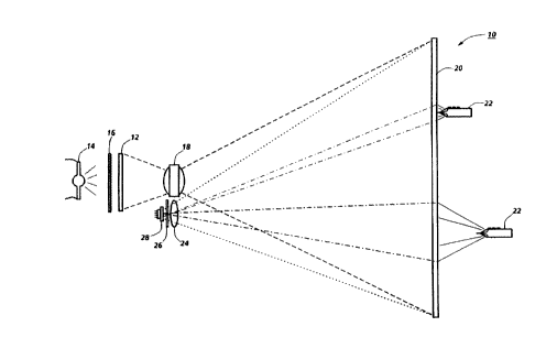
Turning now to the drawings, there is illustrated in Figure 1 a large area
display terminal 10 in the form of a rear projection system comprising a one
million pixel liquid crystal light valve panel 12, controlled by a computer
(not shown). The panel 12 is interposed between a high intensity projection
lamp 14, such as a 650 watt Xenon arc lamp, focused by fresnel lens 16, and
a 270mm projection lens 18. The image is magnified about fivefold to
illuminate, at about twenty spots per inch, a slightly convex curved (as
viewed) display screen 20 having an area of about three feet by five feet. The
screen 20 is preferably made of plastic and is etched to diffuse light for
providing sufficient non-directionality to the viewing angle so that viewers
need not be located directly in front of it.
One or more wireless light pen 22 (two shown) projects a beam of infrared
(IR) light from a light source such as an LED onto the front surface of the
screen 20 at a location where the user desires to indicate input, such as,
locating a pointer. Being wireless, the pen has enhanced usability as a
2051204
collaborative tool since the pens can be used as light spot projection devices
at optimum distances between the screen surface and several feet from it.
When the user is writing upon the screen it is preferable to maintain the
light pen in contact with the surface being written upon. However, when the
user is merely pointing or activating window or menu items upon the screen,
it would be quite practical to project the light spot from several feet away
from the screen. It should be noted that as a remote pen projects a larger
light spot, the effective zone of accurate usage gets closer to the center of the
screen because too much light falls of~ the screen. With wired pens and
multiple users, the wires would probably get tangled in this collaborative
mode of usage.
IR projected light is used, together with an IR sensitive sensor (to bedescribed), so as to minimi7e the amount of interference from spurious light
sources. For safety reasons, the light beam projected from the light pen 22
should be significantly divergent, rather than being collimated. A light pen
having a projection half-angle at half-intensity of about 25~, held about t~vo
feet from the screen, will project a usable IR light spot about two feet in
diameter upon the three by five foot ~creen.
As the IR light spot on the screen is not in the visible range, the user's
feedback is solely the fee-lh~ck generated by the electronic system and
presented on the display (e.g. the pointer) which is obtained by the sensor
and suitable electronics. A large curvature demagnification lens 24, of
about 90x m~gnification, directs the IR light spot through an IR filter 26
, -
2Q~1204
which blocks out spurious light and then focuses the spot upon a position
sensing photodiode 28, such as the UDT SC25D quadrant detector, from
United Detector Technology of Hawthorne, CA. This device has its highest
sensitivity in the IR range and is a continuous dual axis position sensor that
provides both X and Y axis position information. It senses the centroid of a
light spot and provides continuous analog outputs as the spot traverses the
active area. Suitable electronic instrumentation (to be described) allows the
X,Y coordinates to be separated and displayed as a pointer upon the
projection screen 20. The two foot diameter light spot noted above, when
dem~gnified through lens 24, appears as a projection of about 0.3 inch in
diameter on the 0.74 inch by 0.74 inch active surface of detector 26.
A light pen 22 is more clearly shown in Figure 2. It comprises a tubular
body 30 about 0.75 inch in diameter, comparable in size to a whiteboard dry
erase marking pen. It is cordless and is provided with its own power source,
in the form of two nickel-cadmium rechargeable batteries 32 which,
connected in series, generate about 2.4 to 2.7 volts. The optical output of the
light pen emanates from four LED light sources 34a, 34b, 34c and 34d (only
two shown), such as HEMT-3301 from Hewlett-Packard of Palo Alto, CA,
mounted at the front of the pen around a generally conical tip 36. Each of
the four LEDs emits about 6mw of power, cumulatively about 25mw,
resulting in sufficient intensity to enable a high signal-to-noise ratio. At
such a power level, care must be taken to diverge the light to prevent eye
damage. To this end each LED has a cover lens, resulting in the aforesaid
projection cone half-angle at half-intensity of about 25~. At the rear end of
2Q512~A
the pen there is a suitable recharging connection 38 and a disabling switch
40 which electrically disconnects the light sources from the batteries when
the pen is seated within a recharging recess in a recharging tray (not
shown). The recharging tray is preferably mounted directly adjacent to the
projection screen 20 in order to conveniently house the light pens and to
maintain them at m~lrimum charge at all times.
Three function selection buttons 42, 44 and 46 (front, middle and rear),
comparable to mouse buttons, are conveniently located at the front of the
light pen to be easily accessible to the user during manipulation thereof. Of
course, more or fewer function selection buttons may be provided.
Protruding from the conical tip 36 is a pin 48 sheathed in a Delrin sleeve 50
for ease of sliding movement over the display screen 20 and to limit
scratching of the plastic screen surface. Contact of the tip with the display
activates a tip contact switch 62, via the pin 48, which invokes the same
function comm~n-l as the front button 42, to which it is connected in parallel.
When several light pens are used simultaneously, the output signal of each
one must be differentiable from that of the others so that "marks" of one user
are not confused with those of another. Additionally, since each pen is
provided with three function selecting control buttons 42, 44 and 46, the
output signal representative of each of these, plus a "tracking" function (i.e.
Iight source ON with no button depressed and pen movement is tracked by
the cursor), must be differentiable from all other signals. In order to
differentiate the light pen of each user and the several functions invoked by
g
2 Q ~
each, the light sources are encoded, as by chopping, so that their ouputs are
at different frequencies. As illustrated in Figure 3, the four frequencies,
representative of button states, are closely clustered (about 1% apart) and
the mean frequency for each pen is sufficiently remote from the others so as
to be accurately differentiable at suf~lciently high speed. The mean
frequencies for pen identification are easily electronically distinguishable
from one another by bandpass filtering, while the closely clustered, function
identifying frequencies are sufficiently different from one another to be
differentiable with a frequency-to-voltage converter circuit and subsequent
comparators.
It has been found to be desirable to modulate the light sources at rates above
1000 Hz. For example, the four PEN #1 frequencies could be clustered
around 4480 Hz, the four PEN #2 frequencies around 5830 Hz, and the four
PEN #3 frequencies around 7650 Hz. More specifically, the four button
state frequencies could be as shown in the following table:
PEN#1 PEN#2 PEN#3
Track 4539Hz 5907 Hz 7752 Hz
Middle 4500 5856 7684
Rear 4461 5805 7617
Front 4422 5755 7551
--10--
-
20~12~1
In order to generate the several required frequencies, the LE~s of each pen
are controlled by a chopping circuit 54 mounted upon a circuit board 56
housed within the pen, as illustrated in Figure 4. A crystal oscillator,
causing a crystal 58 to resonate at its natural frequency, comprises the
crystal, its biasing resistor 60 and biasing capacitors 62, and an inverter
comprising a single NOR gate of a 74HC02 high speed CMOS chip 64. Based
upon the exemplary frequencies, set forth in the above table, and the
dividing circuitry (described below), the three custom ~uartz c2ystals (from
Hi-Q of Olathe, KS) which have been selected are 2.05184 MHz, 2.67014
MHz and 3.50370 MHz.
The CMOS chip 64 includes four independent NOR gates. Two additional
NOR gates of the chip are used for button identification. Three inputs R, F
and M, from the rear, front and middle buttons, to two of the NOR gates
enable an output of two bits (A and B), from pins 10 and 13, for identification
of the necessary four button states (i.e. front, middle, rear and tracking). A
dividing circuit comprising three 74HC161 high speed CMOS
counter/divider chips 66, 68 and 70 divides down the crystal resonant
frequency to the four closely clustered frequencies, based upon the variable
A and B bits fed into the first counter/divider chip 66 and the fixed inputs.
The 74HC series chips have been selected because they will operate at low
voltage output of the light pen batteries.
2~512Q~
The first two counters/dividers 66 and 68 are combined in order to divide the
crystal clock signal fed to each, based upon the A and B variable inputs from
the button identification chip 64 (to pins 3 and 4 of counter 66), the fixed
inputs 1, 1 (to pins 5 and 6 of counter 66) and the fixed inputs 0, 0, 0, 1 (to
pins 3, 4, 5 and 6 of counter 68). Their collective count will result in a
divisor, which will be 113, 114, 115 or 116, depending upon the four possible
A and B inputs of 11, 01, 10 and 00, which then will be fed to the last
counter/divider 70 whose second (of four) output port (pin 13) represents a
further division by 4. Thus, in PEN #1 the 2.05184 Mhz input to the
cascaded counters would be divided by 452, 456, 460 or 464 depending upon
which function is invoked. The resultant signals of 4539 Hz, 4500 Hz, 4461
Hz and 4422 Hz enable and disable the transistors 72 (2N2222A) for
choppin~ the light output signal (i.e the modulation is from ON to OFF) from
light sources 34a,34b,34c and 34d.
As has been described, the multiple signals from each light pen are achieved
by chopping the optical output of the pens to produce a family of closely
clustered frequencies. It then becomes necessary to electronically
discriminate among the various frequency components in the photodiode
output. The circuit of Figure 5 schematically illustrates one such technique
wherein narrowband filters are used to separate the X and Y positions of one
light pen from the X and Y positions of another.
2-05121~
Although only a single pen, operated at a single frequency is shown anddescribed, it should be understood that a number of pens (e.g. three) can be
used simultaneously and independently.
The position sensing photodiode 26 includes four (two opposed pairs)
electrodes 76 (X+), 78 (X-), 80 (Y+) and 82 (Y-) each of which generates a
current signal as a function of the light intensity and position of the centroidof the light spot projected thereon. If several pens are being used, they
simultaneously project optical signals chopped at different frequencies. The
output signals from the detector electrodes will be a complex superposition
of square waves at those frequencies. These complex waves will be
separated in the circuit described below wherein only representative signals
for the X-axis are shown. It should be understood that the Y-axis signals are
handled in a ~imil~r manner.
X + and X- square wave current sign~ are converted to voltage signals and
amplified at amplifiers 84 and 86. Initially the principal noise in the system
is the detector noise so care is taken to amplify the signal to a usable level
without introducing noise to the signal. These front end amplifiers are
ultra-low noise devices, OP-27G from Analog Devices of Norwood, MA.
Then both signals pass to standard sum and difference amplifiers 88 and 90
for determining location. The sum of X + and X- will always have the same
phase relationship to the pen modulation and will be a fairly large signal,
while the difference can either be in phase (on one side of the center of the
2~1?~4
detector) or 180~ out of phase (on the opposite side of center). Next, the XsUm
and Xdif~ signals, which include filnl1~mental and higher level harmonic
frequency components (since they are comprised of square waves), are each
passed through a switched capacitor narrow bandpass filter 92 and 94 tuned
to a very narrow predetermined frequency range by a crystal controlled
clock 95 so as to pass the cluster of frequencies for a specific pen. The
outputs of the bandpass filters are sine waves at the first harmonic
frequency. Once again the output signals are amplified by amplifiers 96 and
98 in order to be able more easily to extract amplitude and frequency
information representative of position and function.
If more than a single light pen is used, the pen identification cluster of
frequencies for a given pen could be separated by use of a bandpass filter
whose center frequency would be clock controlled for varying the signal
which will be passed. In this manner, the XSUm and Xdif~ (as well as the
YSum and Ydiff signals) would be scanned and the clustered family of
frequencies would be sequentially passed. It would be better, however, to
use dedicated bandpass filters, each tuned to the expected mean frequency of
the clustered family, in order to keep the speed of the system high. There is
a significant transient which occurs when the switched capacitor filter
center frequency is altered by ch~n~in~ the clock &equency.
The XsUm and Xdif~ sine wave signals then pass to sample and hold circuits
100 and 102 controlled by a signal shunted from the XsUm sine wave. The
shunted signal (C) (note Figure 5a) fires a zero crossing detector 104 so that
20512Q4
each time the sine wave (C) crosses zero, the output signal changes between
low and high (0 to 5 volts) as represented by signal (D). When signal (D)
goes from high to low it fires a crystal controlled time delay circuit 106
whose output is signal (E), a negative-going pulse, approximately 511s in
duration, which coincides with the next peak of the sine wave. The time
delay is set to correspond to 1/4 cycle of the mean frequency of the cluster.
Signal (E) controls the sampling of the sample and hold circuits 100 and 102,
(AD583 from Analog Devices of Norwood, MA) so that at every negative
going pulse a peak is sampled. Since the XSUm~ Xdjf~, YsUm and Ydiff signals
are all generated by a single light pen, it is sufflcient to generate a single
timing signal (E) for all of these signals. The output signal (F), from the
sample and hold circuits, is a stair stepping DC voltage indicative of the
amplitude of the XSUm and Xdif~ sine wave signals (C) and (C'), and
representive of the light spot position. Final RC filters 108 and 110 remove
noise from the DC signal (F).
The DC si~n~l~ (F) pass to an analog multiplexer 112 which scans them and
sequentially passes the X~Um, Xdif~, YSUm and Ydiff signals through a unity
gain buffer 113 to an A/D converter 114 which converts each sequentially
received analog voltage signal (F) and converts it into a fourteen bit digital
signal. In the simplest implementation, the 14 bits (two bytes) for each
Xsum, Xdiff, Ysum and Ydif~ signal are passed by an RS232 digital controller
116 to the host computer, such as a SPARCStation-I from Sun Microsystems,
of Mountain View, CA along with the single byte characterizing the button
--15--
2~12Q4
state. Thus, nine bytes are used for a single data point for a single pen. The
sampling time for each data point is about 0.011 sec.
The square wave signal (D) is additionally used to differentiate among the
closely clustered frequencies to determine the invoked function. A portion of
the signal is tapped off and sent to a frequency-to-voltage converter 118
whose output passes to four comparators 120, 122, 124 and 126, each set at a
different threshold in order to determine the exact frequency of the signal
for identifying the button state of the light pen.
Output from the controller 116 feeds back channel select commands to the
multiplexer 112, convert commands to the A/D converter 114, and feeds the
nine bytes of data point information for the single pen to the host computer.
Since both sum and difference signals vary linearly with respect to theintensity of the light spot, a division step will yield generalized X and Y
values (X and Y).
X = Xd~ and Y =--
Xsum Ysum
g and Y eliminate light intensity variability owing to battery power shifts,
the angle at which the light pen is held with respect to the screen, and the
distance of the light pen from the center of the screen. While X and Y have a
one-to-one correspondence with the X,Y location on the screen, they are
generally non-linear with respect to the latter. This arises from non-
linearities in the imaging lens, screen curvature, non-linearïties intrinsic to
--16--
20~1204
-
the detection electronics, and other factors. A calibration procedure is used
to convert x and Y to real X and Y coordinates. A regular grid of points is
displayed on the screen and the x, Y value of each point is measured by
sequentially sampling the points as a light pen is held at that grid location.
Typically, for good calibration, about 200 sampling points on the three by
five foot screen are needed. x, Y values for patches of the screen are fitted toX, Y coordinates using cubic splines. A subsequent linear interpolation is
used to generate a lookup table for the computer.
The preferred circuitry for a system using three light pens fans out from the
X and Y sum and X and Y difference square wave signals. Each of these four
signals is input to each of three dedicated narrow bandpass filters (one for
each mean value of the cluster of pen frequencies). The four output signals
from each narrow bandpass filter are then amplified and the three groups of
signals are passed to three sample and hold circuits, each controlled by a
separate time delay circuit (because the mean values of the frequency
clusters are different). The twelve output DC signals are input to the
multiplexer 112, the A/D converter 114 and then to the host computer.
Additionally, there will be three frequency-to-voltage converters and four
comparators for each converter~ In this manner, the complex X and Y wave
forms from the position sensing photodiode 28 are separated into the
positions and button states of each of the light pens.
Although the present invention has been described with reference to a
specific frquency generating circuit and a specific discrimination circuit, it is
2 ~ D 4
possible that other suitable circuits could be used within the purview of this
invention. For example, for use with multiple pens, the RS232 controller
116 may be eliminated and a microcontroller substituted therefor, whose
output could be sent to the host computer across an RS232 link or be direct
memory access (DMA).
The illustrated embodiment relates to a projection-type computer display
but it should be understood that the nature of the information display may
take other forms as long as the light spots may be projected therethrough
and collected upon a sensor. For example, the display may be a large area
LCD or even a projected slide. In the latter case, the computer of the present
system would generate the image of a pointer whose activity would be
superimposed over the non~omputer generated display.
Further changes are also contemplated. Instead of a single position sensor
receiving the illumination from all of the light pens, several sensors having
the same panchromatic response could be used with color filters to
distinguish the optical output of several light pens, each emitting at a
different color frequency. The function information still could be encoded in
the light pen signal in any desired m,qnner.
Source identity and source function may be impressed on the light pen
illumination in other ways than the described square waves at
predetermined unique chopping frequencies, such as, by distinct coded
sequences of light flashes (illustrated for a single light pen in Figure 6)
--18--
20~1204
representative of the pen source and the selected function. Instead of using
narrowband filters at the expected fundamental frequencies, the processing
electronics would include a set of correlation ~llters for comparing the
transmitted signals to the set of expected codes. The presence of an output
for a given correlation filter would indicate the presence of a particular pen
and function. The amplitude of that output would be related to the X-Y
coordinate of the pen in the same manner as described for the narrowband
filter embodiment. It is also possible to identify the source pen and its
selected function by varying the time duration of the optical pulse (as shown
in Figure 7). In Figure 7a there is illustrated two forms of a sum signal for
the combined inputs of the three light pens for different phase relations
between the pens. The unique pulse width for each light pen and function
could be as shown. By detecting the times and heights of the transition
levels in the sum signal, the processing electronics would be able to extract
the G, H and I signal components and to determine the amplitude of the
signal (indication of position) due to each individual pen.
Therefore, it should be understood that the present disclosure has been made
only by way of example and numerous changes in details of construction and
the combination and arrangement of elements may be resorted to without
departing from the true spirit and scope of the invention as hereinafter
claimed.
--19--