Note: Descriptions are shown in the official language in which they were submitted.
B KGROUND O THE INVENTION
Field of the Invention:
The present invention relates to a bidirectional light waveguide
telecommunication system and more particularly to such a system which employs a
plurality of telecommunication equipment that each comprise a combined opto-
electrical receiving/transmitting module including a laser circuit which is provided with
a monitor photodiode which is used for the dual purpose of acting as a receiver and
as a monitor and, in addition, is utilized for controlling the operating point of the laser
diode by way of a frequency-separating filter connected to the monitor diode which is
connected to a demodulator for the received signals and a control circuit for controlling
the operating point of the laser diode.
Description of the Prior Art
Recent developments in telecommunications technology have lead to
light waveguide telecommunication systems wherein the light waveguides can be
respectively utilized in both transmission directions. In this connection, one is referred
to Geisler, Beaven and Boutruche, ~Optical Fibers~, EPO Applied Technologies Series
Vol. 5, 1986, pp. 552---586, namely in isopositional wavelength operation upon
employment of, for example, direction-separating filters constructed with a partially-
reflecting mirror or an (integrated optical) directional coupler (see Soejima, Yamashit
and Kuwahara, Zurich Seminar '86 Conf. Paper B3, pp. B3.1--B3.8, Section 1 in Table
1), or in wavelength separation mode, i.e. in what is referred to as bidirectional
wavelength multiplex (WDM-Wavelength Division Multiplex) upon utilization of
appropriate wavelength filters ~Zurich Seminar '86 Conf., Paper B3, pp. B3.1-B 3.8,
Section 3 in Table 1), in that light waves having a shorter wavelength are employed for
the signal transmission via (preferably monomode) optical fibers in the one
~(~5~2~5
transmission direction and light waves having a longer wavelength ar~ employed for
the signal transmission in the other transmission direction. In both instances,
appropriate optical separating fil~er module~ are ~o be provided at the two ends of the
light wave guide, these modules respectively effecting a separate light-guiding
connection from the light waveguide to th0 respective op~o-electric transducer and
from the respective electro-optical transducer to the light waveguide. Direction-
separating filters can also be provided in combination with a time separation mode
(Zurich Seminar '86 Conf., Supra, Section 4.1 in Table 1), whereas, conversely, no
additional direction-separating filters need be provided given the time separation mode
when the light-emitting diode or, respectively, a monitor photodiode provided for
controlling the operating point ther00f is also utilized as a receiving diode (Zurich,
Seminar '86 Conf., supra, Section 4.3 in Table 1; German published application 3~ 22
803 A1, published May 3, 1989).
The introduction of new telecommunication systems having light
waveguide (LWG) line trunks or central office lines is quite generally dependent on the
type and scope of the telecommunication infrastructures already existing, together with
the telecommunication services offered therein, and on the demand for new
broadband communication services. The potentially-greatest volume of connections is
thereby envisioned in the domain of private households; this potential for connections,
however, will not be reflected in an effectiv~ demand for connections without
correspondingly^low costs of a broadband subscriber connection.
It has already been provided (European Patent Application 89 117 968,1)
in this context in a bidirectional light waveguide telecommunication system for
wavelength division multiplex (bidirectional WDM) between a central telecommunication
location and a plurality of decentralized telecommunication locations, particularly
having a passive LWG bus network extending between a switching center and a
plurality of subscriber locations, that an electro-optical transmission element and an
opto-elec~ric transmission reception element that are designed for wavelength division
multiplex are provided only the central telecommunication location, whereas a
combined opto-electric receiving/electro-optic transmission module that is fr0e of
wavelength filters, works in the time separation mode and is designed for the emission
of light having a wavelength for whose reception the central telecommunication
location is equipped is respectively provided in the decentralized telecommunication
Iocations, this combined module being formed with a laser module provided with a
monitor photodiode which is utilized as a receiving diode in alternation with its
monitoring function. Due to the signal running time and dependent on the first data
rate and the burst length, however, the distance that can be bridged in a time
separation mode is fundamentally limited
SUMMARY OF THE INVENTION
The object of the present invention, therefore is to avoid such a limitation
and further disadvantages of a time separation mode (such as, for example, the
increased expense for intermediats storing and system control combined with an
additional signat running time that is inadmissible in many instances) for a directional
LWG telecommunication system having a plurality of telecommunication equipment that
respectively comprise a combined opto-electrical receiving/electro-optical transmitting
module having a laser module provided with a monitor photodiode which is also
utilized as a receiving diode in addition to be utilized for controlling the operating point
of the laser diode.
The above object is achieved, according to the present invention in an
LWG telecommunication network in which the telecommunication equipment work in
the wavelength division multiplex mode in that a modulation circuit preceding the laser
~s~
transmission diode converts the electrical transmission signal into a frequency band
other than the frequency band occupied by the electrical receiving signal and a
~requency-separating filter following the monitor diode has its output for signals of the
received signal frequency band ieading to a demo~ulation circuit for the received
signal and has its output for signals of the transmission signal frequency band leading
to a control circuit for the operating point of the laser transmission diode.
In a LWG telecommunication system of the type set forth above, the
present invention yields the advantage of enabling duplex traffic even while avoiding
both an involved wavelength division multiplex mode as well as a time separationmode without having to respectively provide a separate receiving diode having anoptical splitter and the appertaining fiber couplings for that purpose.
BRIEF DESCRIPTION OF THE DRAWING
Other objects, features and advantages of the invention, its organization,
construction and operation will be best understood from the following detailed
description, taken in conjunction with the accompanying drawings, on which:
FIG. 1 is a schematic illustration of.a laser module provided with a
monitor photodiode and located within a LWG telecommunication equipment;
FIG. 2 is a circuit representation of an exemplary embodiment of a
combined opto-electrical receiving/electro-optical transmitting module of the present
invention formed with such a laser module; and
Fl~i. 3 is a schematic representation of a passive optical
telecommunication system having a plurality of telecommunication equipment
.
%~15
constructed and operating in accordance with the present invention.
DE$CRIPTION OF THE PREFERRED EMBODIMENTS
Referring to FIG. 1, a LWG telecommunication equipment TSt is illustrated
that is connected to a light waveguide LWL and that comprises a laser module M
which is provided with a laser transmitting diode SD and with a monitor photodiode
MD as disclosed, for example, in the publication Telcom Report Vol 10, 1g87, Special
"Multiplex-und Leitungseinrichtungen, pp. 146-150, FIG. 4. The laser transmission
diode SD thereby conver~s electrical transmission signals into optical signals to be
transmitted away from the telecommunication equipment TSt via the light waveguide
LWL. In addition to be employed for controlling the operating point for the laser
transmission diode SD, here the monitor diode MD is also utilized as a receivin~ diode
that converts optical signals to be transmitted via the light waveguide LWL to the
telecommunication equipment TSt into electrical received signals. With its two
photoelectrical diodes SD, MD, the laser module M (FIG. 1) is thereby a portion of
combined optoelectrical receiving/electro-optical transmitting module e l o as outlined in
terms of further circuit-oriented details in FIG. 2 as an example.
According to FIG. 2, the optical received signal transmitted via the
lightwave LWL to the opto-electrical receiving/electro-optical transmitting module c¦ o,
just like a portion of the optical transmission signal transmitted by the laser
transmission diode SD and to be transmittecl from the opto-electrical receiving/electro-
optical transmitting module e l o via the light waveguide LWL, proceeds to the monitor
diode MD where the optical signals are converted into corresponding electrical signals.
By way of a receiving amplifier V, the monitor diode MD is followed by a frequency
separating filter FW that has one output e for the electrical reception signal leading to a
received signal demodulation circuit Dem whose output is assumed to form the
electrical output a of the opto-electrical receiving/electro-optical transmitting module
e l o. The frequency separ~tlng fjJter FW is thereby constructed such that it is just
capable of transmitting the frequency band occupied by the modula~ed electrical
reception signal to its output e.
The frequency separating filter FW has a second output s leading to a
control circuit A for the operating point of the laser transmitting diode SD with which
the light current emanating from the laser ~ransmitting diode SD is controlled, as is
known per se; this therefore need not be set forth in greater detail herein.
The frequency separating filter FW, that can be fashioned as a simple
high-pass/low-pass circuit, is capable of transmitting to this output s in a frequency
band other than the frequency band occupied by the modulated electrical reception
signal, namely in a frequency band that is occupied by the electrical transmission
signal supplied to the laser transmitting diode SD. In such a frequency band, other
than the frequency band occupied by the electrical reception signal, in particular, the
electrical transmission signal is eonverte~ in a rnodulator Mod preceding the laser
transmitting diode SD, via the control circuit A for the operating point thereof in the
example. The input of the modulator Mod is assumed to form the electrical input m of
the opto-electrical receiving/electro-optical transmitting module e l o. The modulation
can thereby be undertaken in such a manner that is standard in line cornmunications
or radio relay systems, for example in the form of an amplitude modulation, in the form
of a frequency modulation or phase shift keying, or according to some other,
potentially multi-stage modulation method, and such methods and the details thereof
are not necessary to be set forth herein in that the same are well-known in the art.
The desired frequency separation of the (electrical) reception signal and
the (electrical) transmitting signal is thereforr achieved in the telecommunication
~35
equipment TSt (FIG. I) that contains the opto-electrical receiving/electro-optical
transmitting module e l o (FIG. 2), so that the telecommunication equipment TSt can
implement duplex traffic via the light waveguide LWL. Without this b~ing shown in
greater detail on the drawings, the light waveguide LWL terminated at its one end with
the telecommunication equipment TSt (FiG. 1) can be terminated at its other end with
a corresponding telecommunication equipment, so that the bidirectional LWG
telecommunication system then has the form of what is referred to as an optical link.
The present invention, however, is not limited to such a bidirectional LWG
telecommunication system; on the contrary, for example, it is also possible that the
telecommunication equipment TSt (FIG. 1) and the light waveguide LWL also belong to
an optical local area network (LAN) or that the telecommunication location TSt is a
matter of a decentralized equipment (subscriber location or what is referred to as a
distant unit that combines a plurality of subscriber locations) of a passive optical
telecommunication system in which a respective plurality of such decentralized
equipment are each respectively connected via a separate light waveguide line trunk
tcentral office line) to a light waveguide connection of a central equipment, particularly
represented by a switching center, or to an optical brancher that is connec~ed to a
common light waveguide terminal of the central equipment via a light waveguide bus,
either directly or by way of at least one further optical brancher, as also outlined in FIG.
3.
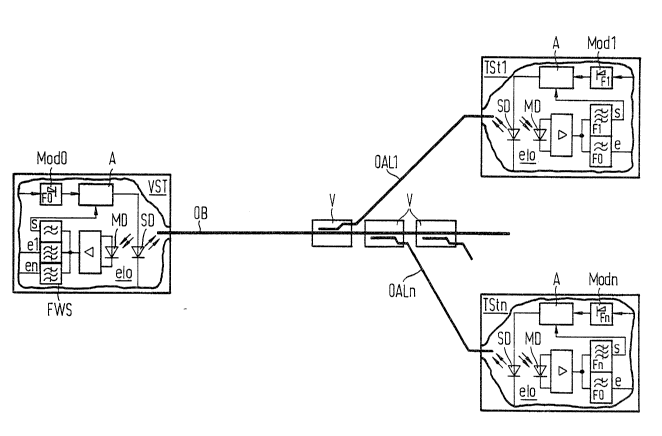
In the bidirectional LWG telecommunication system schematically
illustrated in FIG. 3, a passive (preferably monomode) LWG bus network extends
between a central telecommunication equipment VST that, for example, can involve a
switching center and a plurality of decentralized telecommunication equipment TSt1,....
TStn. Such decentralized telecommunication equipment can be subscriber locations,
or can also be what are referred to as remote units, i.e. interface equipment provided
with an electro-optical/opto-electrical transducer that, with the assistance of a
2~5~25
multiplexer/demultiplexer that lies at the electrical side of the transducer and that is not
shown in further detail in FIG. 3, are capable of combining or, respectively, splitting up
to 32 integrated subscriber digital network (ISDN) B channels, as warranted.
In this LWG telecommunication system, the decentralized equipment T~t
are connected via a single fiber LWG bus OB to a common LWG multiplex terminal of
the central telecommunication equipment DSt. It is assumed that the LWG line trunks
(or central office lines) OAL1,...0ALn belonging to the individual decentralized
equipment TSt1,..., TStn be thereby connected to the appertaining LWG bus OB via
passive optical branches V, namely either directly or via further branches of this type.
For example, tandem mixers or optical directional couplers can thereby be employed
as optical branchers. It is also possible to provide a common optical brancher for a
plurality of light waveguide trunk lines OAL, as known per se ffor example, from the
European patent application 0 171 080). This, therefore, need not be set forth in
further detail herein.
In the telecommunication system outlined in FIG. 3, it is assumed that the
individual telecommunication equipment TSt1,..., TStn and VSt are each respectively
provided with an opto-electrical receiving/electro-optical transmitting module e l o, as
was already set forth in principle with reference to FIG. 2. A respective laser
transmitting diode SD and a monitor diode MD, as utilized as a receiving diode at the
same time, are therefore respectively provided, this being followed by a rec0iving
amplifier VA, but a frequency separating filter circuit FWS that has an output s for
signals of the respective transmission signal frequency band leading to th0 control
circuit A for the operating point of the laser transmitting diode SD, and that has an
output e for signals of the respective receiving signal frequsncy band respectively
followed by a demodulation circuit (not shown in FIG. 3, see FIG. 2) for the
appertaining received signal.
;~5~
A frequency division multiplex mode is provided as foll~ws for separating
the directions in the telecommunication system illustrated in FIG 3:
For signal transmission in the downstream direction, i.e. from the central
telecommunication location VSt to the decentralized telecommunication
locations TSt1,...TStn, the modulation circuit MD0 that precades the laser
transmitting diode SD of the central telecommunication location VST
oonverts the electrical transmission signal into a frequency band F0
whose signals raspectively proceed to the frequency separating filter
output e in the decentralized telecommunication locations TSt1,..., TStn
and, therefore, proceed to the respective following demodulator
Mod1,. .. ,Modn.
In the opposite transmission direction it is assumed that the modulators
Mod1,....Modn of the decentralized telecommunication equipment TSt1,...,TStn convert
the respective electrical transmission signal into a frequency F1,...,Fn respectively
individually associated to the telecornmunication equipment with a corresponding
plurality of frequency bands that each respectively differ from the aforementioned
frequency band F0 that is occupied by the respective electrical reception signal in all
decentralized telecommunication equipment TS~1,...,TStn in ~he sarne manner. In the
central telecommunication equipment VST, the monitor diode MD is then not only
followed by a simple frequency separating filter having two outputs, but is also followed
by a frequency separating filter FWS' having a corresponding plu;ality of outputs
e1,...en for signals of the m0ntioned frequency bands F1,...Fn that are indiv7dually
associated to the remote telecommunication equipment. The outputs e1,...,en each
respectively lead to a demodulator (not shown in FIG. 3, but of the sama type
illustrated in FIG. 2, allocated to the respective frequency band for the reception signal
., .
5~
resulting from the appertaining, decentralized ~elecc: mmunication equipment. The
output s of the ~reqùency separating filter for the signals of the transrnission signal
frequency band F0 of the centralize~ telecommunication sqùipment VSt, in turn, leads
to the control circuit A thereof for the operating poin~ of its laser transmitting diode SD.
One therefore not only obtains the desired frequency-division multiplex signals
transmitted in the downstream direction, on the one hand, and signals transmitted in
the upstream direction, on the other hand, but rather, at the same time, an upstream
transmission of signals of different decentralized equipment executed in frequency-
division multiplex is also obtained at the same time, this by comparison to a time-
division multiplex or, respectively, TDMA operation that is also inherently possible, and
requires no synchronization expense or, respectively, delay expense for observing
prescribed time slots.
Although I have described my invention by reference to particular
illustrative embodiments thereof, many changes and modifications of the invention may
become apparent to those skilled in the ar~ without departing from the spirit and scope
of the invention. I therefore intend to include within the patent warranted hereon all
sùch changes and modifications as may reasonably and properly be included within
the scope of my contribution to the art.