Note: Descriptions are shown in the official language in which they were submitted.
20S129~
QUASI-PHASE MATCHING
OPTICAL WAVEGUIDE
F;el~ of the Tnvent;on
The invention relates to optical waveguides.
S More specifically, this invention relates to optical
waveguides of the type used to convert a polarized
laser beam to a frequency doubled (second harmonic)
wavelength.
Brief DescriDtion Qf the DrAwings
Figure 1 is a schematic diagram of a quasi-
phase matching optical waveguide showing features which
the waveguide of the invention shares with prior art
waveguides.
Figure 2 is a cross-sectional view of a prior
art conventional waveguide showing distortions in
spacing attributable to field spreading.
Figure 3 is a cross-sectional view of a
waveguide satisfying the requirements of the invention.
Figure 4 is a cross-sectional view of an
alternate embodiment of a waveguide satisfying the
requirements of the invention.
Figure 5 is a sectional view of a~ additional
embodiment of a waveguide satisfying the requirements
of the invention.
2S RAck~rolln~ of the Invent;on
This invention is an improvement on the
quasi-phase matching optical waveguide disclosed by
Khanarian et al U.S. Patent 4,865,406.
The present invention shares with Khanarian
et al the objective of providing a quasi-phase matching
optical waveguide capable of converting polarized light
from a laser to its second harmonic--i.e., doubling the
CAS83118.DOC
205129~
frequency of the light being propagated through the
waveguide.
A schematic arrangement capable of satisfying
this objective is schematically shown in Figure 1. A
S laser source 1 is provided offering transverse magnetic
(TM) polarized light having a wavelength in the range
of from about 700 to 1300 nm. The light source is
monochromatic--that is, confined to a single wavelength
or narrow band of wavelengths. The laser beam 3 is
directed through an optical coupling element 5 (shown
as a prism) to an optically active layer unit 7 mounted
on a support 9. In laterally spaced areas 11 indicated
by vertical arrows the optically active layer unit
contains organic molecular dipoles which are in polar
lS alignment. In intervening areas 13 the organic
molecular dipoles are either randomly oriented or
exhibit a polar alignment opposite that of areas 11.
After passing sequentially through a
plurality of areas 11 and 13, light passes through
output optical coupling element 15 (shown as a prism)
as indicated by arrow 17 to a conventional utilization
apparatus responsive to the second harmonic (frequency
doubled) component of the input light.
For efficient conversion of the input light
to its second harmonic to occur it is essential that
the light path in each of the areas 11 and 13 be of
identical length and each equal to one coherence length
(ec)- While K~n~rian et al postulated this
relationship and schematically illustrated it,
Khanarian et al was unable to achieve this required
relationship in the waveguides actually demonstrated.
The construction difficulties which Khanarian
et al encountered are illustrated in Figure 2.
Referring to Example 1 of Khanarian et al, a silicon
wafer 21 is shown provided with a silicon dioxide layer
CA583118.DOC
205~2~0
23. On the silicon dioxide layer are formed a spaced
lower array of aluminum electrodes 2S, each 0.1~m
(1000A) in thickness.
Over the aluminum electrodes a 1.5 ~m lower
S cladding layer 27 is coated. A nonlinear optically
active organic layer 29 of 1.65 ~m in thickness is
coated over the lower cladding layer. An upper
cladding layer 31 of 1.5 ~m in thickness is coated over
the optically active layer. The organic optically
active layer 29, the lower cladding layer 27, and the
upper cladding layer 31 together form an optically
active layer unit. Overlying the upper cladding layer
is an upper array of aluminum electrodes 35 having a
thickness of 0.055 ~m.
Even if it is assumed that ~n~rian et al
actually achieved the formation of lower electrodes 25
having a width of one coherence length (~c) and spaced
by a width of one coherence length, it does not follow
that the width and spacing of areas in the optically
active organic layer 29 adjacent the electrodes were
also one coherence length in width and spacing.
Several difficulties are encountered in
attempting to satisfy the performance characteristics
sought by Khanarian et al with the construction of
Figure 2. To achieve polar alignment of organic
molecular dipoles within the optically active layer in
areas adjacent the electrodes as schematically
indicated by arrows 37 Khanarian et al raised the
temperature of the optically active layer unit to a
temperature sufficient to allow freedom of movement of
organic molecular dipoles contained in the organic
optically active layer 29, thus producing organic
layers with liquid properties. With organic optically
active layer unit heated a potential difference was
CAS83118.DOC
20512~0
applied between the electrodes 25 of the lower array
and the electrodes 35 of the upper array.
A first difficulty which is encountered with
the construction of Figure 2 is that the electrical
S field between the oppositely biased electrodes of the
upper and lower arrays was not confined to areas of the
organic optically active layer corresponding in width
to the width of the electrodes. In other words,
significant field spreading occurred, as indicated by
boundaries 39. Within the boundaries the organic
molecular dipoles exhibited polar orientation.
However, because of lateral spreading of the electrical
fields, the areas of the organic optically active layer
which contain polar aligned organic molecular dipoles
are much larger in width than intervening areas in
which the organic molecular dipoles are not polar
aligned, and neither the polar aligned areas nor the
intervening areas correspond in width to electrode
widths. Even if the electrodes were successfully
fabricated to be one coherence length in width, as
sought, then it is apparent that neither the areas of
the organic optically active layer containing polar
aligned organic molecular dipoles or the intervening
areas of this layer are one coherence length in width.
A second difficulty is that the cladding
layers increase the spacing between the electrodes,
thereby reducing the potential gradient within the
optically active layer. Only the potential gradient
within the optically active layer contributes to polar
alignment of the organic molecular dipoles. Therefore,
higher potential biases must be placed across the
electrodes when effecting polar alignment of the
organic molecular dipoles or the degree of poling of
the organic molecular dipoles will be reduced.
CAS83118DOC
20512~0
Another difficulty with the construction of
Figure 2 is that the electrodes 35 of the upper array
are during heating and poling floating on underlying
layers heated to exhibit liquid properties. The result
is that the slightest touch or tilt of the device while
heated can contribute to shifting the placement of one
or more of the electrodes 35 on the organic layer unit
laterally, destroying the coherence length spacing
being sought.
Snmm~ry ~f the Inv~ntion
The present invention overcomes a number of
disadvantages exhibited by prior art quasi-phase
matching optical waveguides. Most fundamentally, the
present invention offers a more precise match between
the width and spacing of areas of the organic optically
active layer in which organic molecular dipoles are
oriented in polar alignment and the width and spacing
of electrodes of an underlying array. With the present
invention the width and spacing of the polar aligned
areas of the organic optically active layer are more
precisely controlled.
In a specifically preferred embodiment of the
invention the necessity of employing cladding layers is
entirely eliminated. In addition to simplifying
construction, this allows the entire potential
difference used in poling the organic molecular dipoles
to occur within the optically active layer, thereby
increasing its internal potential gradient for a given
applied electrical potential difference. It is also
possible to entirely eliminate the upper electrode
array, thereby obviating any concern about electrode
shifting while poling organic molecular dipoles in the
organic optically active layer.
In addition, in one preferred form the
invention offers a very simple and advantageous
CA583118.DOC
2~512!~0
--6--
approach for providing interleaved (i.e.,
interdigitated or alternated) areas of oppositely poled
organic molecular dipoles within the organic optically
active layer.
In one form the invention is directed to a
quasi-phase matching optical waveguide for producing a
second harmonic of an internally propagated polarized
laser beam having a wavelength in the range of from 700
to 1300 nm comprised of means for providing at least a
first array of electrodes with next adjacent electrodes
being laterally spaced in the direction of propagation
of the laser beam and organic layer means for
propagating the laser beam containing organic molecular
dipoles exhibiting a first polar alignment in areas
lS overlying the electrodes of the first array to provide
a second order polarization susceptibility in excess of
lO 9 electrostatic units.
The waveguide is characterized in that the
electrodes of the first array are in direct contact
with the organic layer means and are chosen to exhibit
a refractive index with an imaginary component of less
than O.l and a conductivity at least 5 orders of
magnitude higher than that of the organic layer means
and the electrodes of the first array and the areas of
the organic layer means exhibiting the first polar
alignment each have the same width and spacing.
DescriDtion Q~ Preferre~ ~mhodiments
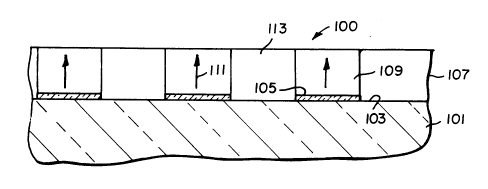
A quasi-phase matching optical waveguide lO0
according to the invention is shown in Figure 3. A
transparent support lOl, such as a glass or quartz
substrate, has positioned on its surface 103 an array
of electrodes 105 that each exhibit the same width and
spacing from the next adjacent electrode. Contiguously
overlying the surface 103 of the support and the
electrode array is an organic optically active layer
CAS83118DOC
2051290
107 containing organic molecular dipoles. The support
103 has a refractive index less than that of the
optically active layer 107. The optically active layer
is divided into a plurality of areas 109 each overlying
S one of the electrodes of the array and corresponding to
the underlying electrodes in width and spacing. In
each of the areas 109 the organic molecular dipoles are
polar aligned, as indicated schematically by arrows
111. Areas 113 in which the organic molecular dipoles
are not in polar alignment separate next adjacent areas
109 .
Comparing the waveguide 100 of the invention
with the prior art waveguide shown in Figure 2, a
number of differences are apparent. First, the
waveguide 100 is simpler in construction, containing
only one array of electrodes and no cladding layers.
Second, there is a better correspondence between the
width and spacing of the electrodes 105 and the areas
109 of the optically active layer containing polar
aligned organic molecular dipoles.
Elimination of an array of electrodes
overlying the optically active layer and a cladding
layer separating the overlying array of electrodes from
the optically active layer is made possible by placing
a static electric charge on the upper surface of the
organic optically active surface during poling while
concurrently placing an opposite polarity bias on the
electrodes 105. This places a voltage drop across the
optically active layer in areas corresponding in width
to the underlying electrodes. Field spreading, as
shown in Figure 2, is curtailed because the field
gradient is applied across only a single layer as
compared to three separate layers, which together
approximately triple the distance between the biasing
charge sources.
CA583118.rPDC
20512~0
--8--
The elimination of a lower cladding layer
separating the organic optically active layer and the
underlying electrode array is made possible by specific
selection of materials forming these electrodes. First
and most fl~n~mentally, the electrodes must, of course,
be formed of a material having an electrical
conductivity that is high in relation to that of the
organic optically active layer. The electrodes 105
have a conductivity that is at least 5 orders of
magnitude higher than that of the organic optically
active layer, preferably the conductivity of the
electrodes is at least 10 orders of magnitude higher
than that of the optically active layer.
A second requirement of the electrodes 105 is
lS that they must be formed to be compatible with guiding
light in the organic optically active layer. While
metals generally impart the required conductivity level
for electrode construction, all metal electrodes must
be excluded from consideration because of their
creation of large optical losses within the waveguide.
Electrodes 105 are formed of a material satisfying the
above stated conductivity requirement and also
exhibiting a refractive index compatible with
efficiently guiding light in the optically active
layer.
In considering the refractive index of an
electrical conductor two components must be considered,
the real component and the imaginary component. To
confine light efficiently to the optically active layer
it is preferred that the real component to the
refractive index be less than the refractive index of
the optically active layer. In this respect the
selection of the material to form the electrodes is not
different than selecting any of the various dielectric
materials, including air, contacting the optically
CA583118DOC
20512~0
active layer, since a dielectric material can be
thought of as having a refractive index consisting of a
real component and an imaginary component which is
essentially zero.
S If the thicknesses of the electrodes are
small--e.g., less than about 200A, the real component
of the refractive index of the material forming the
electrodes can be ignored. Even if the real component
of the refractive index is higher than that of the
optically active layer, thereby allowing a portion of
the laser beam to enter the electrodes, the limited
thickness of the electrodes insures that most of the
laser beam will continue to be propagated within the
optically active layer.
lS The imaginary component of the refractive
index of the electrode forming material is important,
since this controls absorption of light being
transmitted within the optically active layer by the
electrodes. A quantitative criterion for selection of
a material for the electrodes 105 exhibiting a low
light absorption is provided by the imaginary component
(customarily assigned the subscript i) of the
refractive index of the material. The electrodes of
the waveguides of this invention which lie in direct
contact with the organic optically active layer are
chosen to exhibit a refractive index imaginary
component of less than 0.1, preferably less than 0.01.
The waveguide 100 is an illustration of one
preferred waveguide construction satisfying the
requirements of the invention. Other waveguide
constructions meeting the requirements of the invention
are contemplated.
An alternative waveguide construction is
shown in Figure 4. Waveguide 200 consists of a support
shown having a base portion 201 and an optically
CAS83118.DOC
20~129~
--10--
transparent overlying portion 202. Located on the
upper surface 203 of the overlying portion of the
support is a conductive layer 205. Transparent
electrically insulative segments 207 are located on the
S conductive layer. The insulative segments are
laterally spaced by a distance equal to their width.
Overlying and in direct contact with the insulative
segments and the areas of the conductive layer lying
between the insulative segments is an organic optically
active layer 209. The organic molecular dipoles in the
organic optically active layer are oriented in polar
alignment, as indicated schematically by arrows 211, in
areas 213 located between the insulative segments. In
areas 215 of the optically active layer the organic
lS molecular dipoles are not oriented in polar alignment.
Comparing the waveguides 100 and 200, it is
apparent that the conductive layer 205 and insulative
segments 207 together form a pattern of electrodes in
direct contact with the optically active layer 209 in
areas 213 between the insulative segments. The
conductive layer 205 in areas of contact with the
optically active layer must satisfy the same
requirements as the electrodes 105 and is contemplated
to be constructed from the same materials. The
2S conductive layer 205 is shown as a continuous layer of
uniform composition, since this is the most convenient
form for fabrication; however, it is realized that the
portions of the conductive layer underlying the
insulative segments can be varied in composition or
omitted entirely.
To minimize optical losses in the conductive
layer 205 it is preferred that this layer be quite
thin, typically less than 200A in thickness. However,
such small thicknesses will not isolate the laser beam
in the optically active layer 209 from the support.
CAS83118.DOC
205129~
Therefore, when the underlying portion 201 of the
support is formed of a material that would otherwise
attenuate the laser beam being propagated, it is
important to include the optically transparent
S overlying portion 202 of the support between the
conductive layer 205 and the underlying portion 201 of
the support. The overlying portion can conveniently
take the form of a layer having thickness of about 1 ~un
or more, preferably at least 5 ~m, in thickness.
10 Alternatively, the entire support can be optically
transparent, as described in connection with Figure 1.
When the support portion 202 is constructed
as indicated, the support portion 201 can be formed of
any convenient material having the structural integrity
lS to form a unitary substrate, including any electrically
conductive, insulative or semiconductive material and
any material that is either optically transparent,
absorptive or opaque.
When the conductive layer is formed as shown
20 as a continuous, uniform layer underlying the
insulative segments, the electrically insulative
segments are formed of materials that have a high
resistivity (low conductance) as compared to that of
the organic optically active layer. The reason for
25 this is that during electrical biasing to bring the
organic molecular dipoles into polar alignment the
entire conductive layer is at one electrical potential
level while the static charged surface of the organic
optically active layer is at a second electrical
30 potential. To restrict poling to areas 213 located
between the insulative segments it is necessary that
the insulative segments account for almost all of the
voltage drop between the conductive layer and the
charged surface of the optically active layer. A
35 satisfactory division of the total voltage drop between
CAS83118.DOC
2051290
-12-
each insulative segment and the overlying portion of
the optically active layer in each area 215 can be
achieved by forming the insulative segments of
materials that have a resistance at least 2 orders of
S magnitude higher than (or a conductivity at least 2
orders of magnitude lower than) that of the material
optically active layer. The relative resistances of
the insulative segments and the overlying portions of
the optically active layer are recognized to be a
function of both relative resistivities and relative
thicknesses.
Apart from the differences in features
specifically discussed, the waveguide 200 offers
essentially the same advantages over the waveguide of
Figure 2 as those described above in connection with
waveguide 100.
In the waveguides 100 and 200 areas 109 and
213, respectively, are shown containing organic
molecular dipoles in polar alignment interleaved with
areas 113 and 215, respectively, in which the organic
molecular dipoles are not oriented in polar alignment.
~h~n~rian et al, cited above, schematically suggests
constructing a waveguide in which adjacent areas of the
optically active layer contain organic molecular
dipoles in oppositely oriented polar alignments;
however, no example or general guidance for producing
such an arrangement is provided.
The present invention specifically
contemplates a waveguide in which interleaved areas of
the optically active layer contain organic molecular
dipoles in oppositely oriented polar alignment. An
illustrative, practical construction, is shown in
Figure 5 in the form of waveguide 300. A support 301
is provided which can be formed of any convenient
material (e.g., any material useful for fabricating
CA583l18.DOC
2051290
-13-
support 201). An electrically conductive layer 303 is
shown on the support. The electrically conductive
layer 303 can take any convenient form, including, but
not limited to, any form described above for conductive
S layer 203. Since the electrically conductive layer 303
need not directly contact the optically active layer,
it is immaterial whether this electrically conductive
layer is optically transparent. When the support 301
is electrically conductive, the conductive layer 303
can omitted, if desired.
Overlying the conductive surface provided by
the conductive layer 303 (or the support 301 when
constructed of a conductive material with layer 303
omitted) is an electrically insulative, optically
1S transparent layer 305. The requirements described
above for overlying portion 202 of the support are
generally applicable to layer 305. Overlying the
transparent insulative layer 305 are electrodes 307,
which can be identical in their construction to
electrodes 105 described above. Organic optically
active layer 309 overlies and is in direct contact with
the electrodes 307 and the intervening portions of the
dielectric layer. Overlying the optically active layer
is an insulative cladding layer 311 and an electrically
2S conductive layer 313. When the electrically conductive
layer 313 is formed of materials having the same
properties as those useful in forming the electrodes
307, the cladding layer 311 is not re~uired.
The organic optically active layer contains
areas 315 overlying the electrodes 307 that contain
molecular dipoles in polar alignment as schematically
indicated by arrows 317. Between the areas 315 are
areas 319 in which the organic molecular dipoles are
also in polar alignment, but, as indicated
3S schematically by arrows 321, in a polar alignment that
CA583118.DOC
2051290
-14-
is oriented opposite to that in areas 315. Each of the
areas 315 and 319 are of equal width.
The waveguide 300 can be constructed by
coating the conductive layer 303 on support 301
S followed by coating the transparent insulative layer
305. Thereafter the electrodes 307 are formed on the
transparent insulative layer, either by patterned
deposition, or by forming a continuous conductive layer
followed by patterned removal.
Next the organic optically active layer 309
is coated over the electrodes and the intervening
portions of the transparent insulative layer. As
coated the optically active layer is in a form in which
the organic molecular dipoles contained therein have
significant mobility. To impart polar alignment to the
organic molecular dipoles in areas 315 a uniform static
charge is imparted to the surface of the optically
active layer and an opposite polarity electrical bias
is placed on the electrodes 307. This creates a field
gradient in the optically active layer that is confined
to areas 315. Because the field gradient is confined
to areas 315, the organic molecular dipoles in this
region alone assume a polar aligned orientation, as
indicated by arrows 317. With the electrical field
applied, the organic molecular dipoles are permanently
locked into their polar aligned orientation. This can
be achieved, for example, by photopolymerizing or
photocrosslinking the organic optically active layer
selectively in the areas 315.
Once organic molecular dipoles in areas 315
have been permanently locked in a polar aligned
orientation, oppositely orienting the organic molecular
dipoles in areas 317 is simple, since the areas 315
necessarily define not only their own width and
spacing, but also the width and spacing of the
CAS83118.DOC
2~51290
interleaved areas 317. Therefore, a variety of poling
techniques can be employed, including those that would
not be suitable for forming the areas 315 with the
required width and spacing.
One approach for achieving a polar alignment
in areas 319 which is the opposite that in areas 315 is
to coat the upper surface of the optically active layer
with the cladding layer 311 and then to coat conductive
layer 313. By placing a potential gradient between
conductive layer 313, serving as one poling electrode,
and conductive layer 303 (or the support 301, when it
is formed of a conductive material) the desired polar
alignment of organic molecular dipoles in areas 319 can
be realized. During this poling step the transparent
lS insulative layer 305 and the cladding layer 311 both
present resistances which are in series with the
organic optically active layer. To place as much of
the voltage drop between the conductive layers 303 and
313 as possible within the organic optically active
layer so that it is available for aligning the organic
molecular dipoles, the resistances of the cladding
layer and the transparent dielectric layer are
preferably kept to a minimum. To this end the
transparent dielectric layer can be formed of an
organic dielectric, such as a polymer, having a
resistivity similar to that of the organic optically
active layer. By keeping the thickness of the
transparent dielectric layer below that of the
optically active layer the resistance of the former can
be further reduced in relation to the latter.
For a quasi-phase matching optical waveguide
to be efficient in producing a second harmonic of the
fundamental light frequency being propagated it is
necessary for the light propagation path to traverse in
the optically active layer one coherence length (ec) in
CA583118.DOC
2051290
-16-
which the organic molecular dipoles are in polar
alignment followed immediately by a second coherence
length in which the organic molecular dipoles are not
polar aligned or oppositely polar aligned. The
S coherence length (~c) is defined by the following
equation:
(I)
~c = (~/~B)
where
~ is 3.1416 and
~ B is the propagation constant difference.
The propagation constant difference is defined by the
following equation:
(II)
lS ~B = IB(2~l)-2B(~l)
where
B is the propagation constant of a mode (e.g., the
zero order mode) and
~ 1 is the fundamental frequency of the light being
propagated.
It is not essential that the interleaved
areas of the organic optically active layer each be
exactly one coherence length in width and spacing for
efficient conversion to the second harmonic frequency
to occur. What is essential is that the width and
spacing of the interleaved areas of the optically
active layer each be equal. Once this relationship is
satisfied the path of the light beam can be oriented in
the optically active layer to the coherence length
satisfying spacing.
This is illustrated by reference to Figure 6,
wherein the bars 401 are of equal width and spacing and
CAS83118.DOC
2051290
-17-
schematically represent areas within an optically
active layer in which the organic molecular dipoles are
arranged in one selected polar aligned orientation.
When a light beam of a selected wavelength in passed
through the organic optically active layer as indicated
by arrows 403, the width and spacing of the bars may be
slightly longer or shorter than one coherence length.
By rotating the light beam clockwise toward the
position indicated by arrows 405 the width and spacing
or the bars as encountered by light beam can be
reduced. By rotating the light beam counter-clockwise
as indicated by arrows 407 the width and spacing or the
bars as encountered by light beam can be increased.
Thus, so long as the poled areas represented by bars
401 are of equal width and spacing the light beam can
be efficiently converted to its second harmonic
frequency even though the width and spacing of the
poled areas does not exactly correspond to one
coherence length. However, it should be noted that if
the width and spacing of the poled areas are not equal,
neither clockwise nor counter-clockwise rotation will
produce optimum results.
The organic optically active layers of the
quasi-phase matching waveguides can be constructed of
any polymeric medium capable of exhibiting a high
(>10 9 esu) second order polarization susceptibility in
areas containing polar aligned organic molecular
dipoles containing an electron donor moiety linked
through a conjugated ] bonding system to an electron
acceptor medium. The organic molecular dipole can
itself form a part of a polymer as a repeating unit in
the polymer backbone or, more commonly, as a pendant
group. Alternatively, the organic molecular dipole can
be present as a separate compound physically blended
with a polymer binder. The polymer portion of the
CA583118DOC
20~1~90
-18-
layer can be either a linear or a crosslinked polymer.
Conventional polymers as well as cladding layer,
dielectric layer, support and other conventional
waveguide component materials satisfying the
S requirements of the waveguides of the invention
additionally including details of forming layers are
taught by Scozzafava et al U.S. Patent 4,946,235 and
Scozzafava et al U.S. Serial No. 419,819, filed Oct.
11, 1989, commonly assigned and now allowed, the
disclosures of which are here incorporated by
reference.
The materials forming the optically active
layers typically exhibit resistivities of at least 1012
ohm-cm, with resistivities ranging two to three orders
of magnitude higher (i.e., up to 1015 ohm-cm) being
common. The organic optically active layer can be
formed in any conventional thickness found in optically
active waveguides capable of frequency doubling.
Preferred layer thicknesses are in the range of from
about 0.1 to 10 ~m, optimally from about 0.5 to 3 ~m.
The materials forming the electrodes lying in
direct contact with the organic optically active layers
are chosen from materials satisfying the conductivity
and refractive index requirements discussed above.
Because of the high resistivity levels of the materials
forming the optically active layers very little current
is conducted during poling. Thus, the electrodes,
which are used only during poling, need sustain only
very small current densities.
Conductive polymers constitute one
contemplated class of materials for forming the
electrodes lying in direct contact with the organic
optically active layers. Conductive polymers and their
properties are disclosed in the Handbook of Conducting
Polymers, Vol. 1 and 2, Terje A. Skothem, editor,
CA583118.DOC
205129~
--19--
Marcel Dekker, Inc., New York, 1986, the disclosure of
which is here incorporated by reference. Organic
conductive polymers that rely on conjugated
unsaturation for conductivity, such as polyacetylenes
S and polyenes, can absorb significant amounts of light
in the visible spectrum. However, even polymers that
appear to the eye to be deeply colored often lack
chromophores capable of absorbing light at the longer
infra-red laser wavelengths contemplated and can be
selected also to exhibit little or negligible
absorption in the wavelength range of the second
harmonic. Polypyroles and polythiophenes and their
derivatives are additional specifically contemplated
classes of conductive polymers.
lS Polymers that are known to be useful in
producing antistatic coatings can also be used as
conductive polymers for forming the electrodes in
direct contact with the optically active layers.
Polyanilines of the type disclosed by Trevoy U.S.
Patents 3,963,498; 4,025,342; 4,025,463; 4,025,691; and
4,025,704, the disclosures of which are here
incorporated by reference, can be selected for forming
the electrodes lying in direct contact with the
optically active layers. Phenazene polymers of the
2s type disclosed by Ferrar et al EP 0 304 296 A3, here
incorporated by reference, are also contemplated for
use. Vinyl polymers with pendant ionic groups, such as
provided by quaternized nitrogen atoms or sulfonic acid
groups, of the type commonly used as dye mordants are
known to be useful as antistatic coatings and can be
used in the construction of the electrodes of the
waveguides of this invention. Vinyl polymers with
pendant ionic groups used to form antistatic coatings
are illustrated by Rese~rch Disclosure, Vol. 158, June
3S 1977, Item 15840; Vol. 162, Oct. 1977, Item 16258; and
CAS83118.DOC
2051290
-20-
Vol. 166, Feb. 1978, Item 16630; the disclosures of
which are here incorporated by reference. Res~rch
D;sclosl~re is published by Kenneth Mason Publications,
Ltd., Dudley Annex, 21a North Street, Emsworth,
S Hampshire P010 7DQ, England.
The electrodes in direct contact with the
optically active layers of the waveguides of this
invention are preferably formed of a conductive metal
oxide. Indium oxide (In2O3) and tin oxide (SnO2) are
specific examples of metal oxides. Indium tin oxide
(mixed crystals of In2O3 and SnO2, commonly designated
ITO) constitutes a specifically preferred metal oxide
electrode material because of its high conductivity and
its low refractive index imaginary component ti).
Typical preferred indium tin oxide compositions contain
5 to 20 percent indium oxide, on a molecular basis,
based on indium and tin oxides.
Since indium tin oxide can be readily
deposited in a form exhibiting a resistivity of less
than 1 X 10 2 ohm-cm, typically approximately 7 X 10⁻³
ohm-cm, it is apparent that the conductivity of the
indium tin oxide is more than sufficient in relation to
that of the optically active layer to form an efficient
electrode even in thin coatings. At a wavelength of
830 nm (n = 1.941-0.001) electrode thicknesses can be
translated into optical losses as follows:
ITO Thickness ;n A oDtical T~oss (~R/cm)
0 . 90
100 1.91
150 3-03
200 4.28
250 5.68
Preferred waveguides according to the invention contain
electrodes in contact with the optically active layer
CAS83118.DOC
2051290
that are formed of indium tin oxide and exhibit a
thickness of less than 150A to 50A, optimally 125A to
75A.
F~1CA~1 es
S The feasibility of the invention is
demonstrated by the following:
An 18 weight percent solution of poly{4'-[N-
(2-methacryloxyethyl-N-methylamino]-4-methylsulfonyl-
stilbene-co-methyl methacrylate} (19:81 mole ratio) in
1,2,3-trichloropropane was prepared. The solution was
spin-coated on a Pyrex substrate with a thin ITO
grating with a grating constant of 11.6 ~m. In other
words, the ITO strips had a width of 5.8 ~m and were
separated by 5.8 ~m spacings. The film was then baked
overnight in a vacuum oven at 115C and 25 mtorr. The
thickness of the film was 2.85 ~m. The polymer was
corona poled with a grid voltage of 350 volts for 1
hour at 108C.
A 514.5 nm beam of an argon ion laser was
guided in the film. The guided beam was not
significantly attenuated as it passed through the
region of the substrate covered by the ITO grating.
The measured effective refractive indices of the TE
modes were 1.5671, 1.5604, 1.5491, 1.5335 and 1.5135.
The measured effective refractive indices of the TM
modes were 1.5660, 1.5590, 1.5476, 1.5318 and 1.5112.
The effective refractive indices can be converted to
propagation constants by multiplying by the wavenumber
of the light beam in free space (l/c, where l is the
angular frequency of light and c is its speed).
A 1064 nm beam of a diode pumped YAG laser
was guided in film. The guided beam was not
significantly attenuated as it passed through the
region of the PyrexTM substrate covered with thin ITO.
The measured effective refractive indices of the TE
CAS83118DOC
2051290
-22-
modes are 1.5267, 1.5013 and 1.4634. The measured
effective refractive indices of the TM modes were
1.5262, 1.5005 and 1.4631.
The difference in the effective refractive
S indices of the lowest order TM modes at 514.5 nm and
1064 nm was 0.0398. This corresponded to a coherence
length (ec) of 6.68 ~m. Based on this coherence length
and the ITO grating constant the TMo mode of a 1064 nm
guided beam was quasi-phase matched to the TMo mode of
a 532 nm beam when the beams were oriented at an angle
of 29.7 degrees with respect to the direction of the
grating.
The invention has been described in detail
with particular reference to preferred embodiments
thereof, but it will be understood that variations and
modifications can be effected within the spirit and
scope of the invention.
CA583118DOC