Note: Descriptions are shown in the official language in which they were submitted.
~- , 1 205 1 453
Long Wavelength Transmitter Opto-Electronic Integrated
Circuit
The present invention relates to a transmitter opto-
electronic integrated circuit (hereinafter referred to as
transmitter OEIC) in which a semiconductor laser and an
electronic device are integrated. More particularly, it
relates to a long wavelength transmitter OEIC in which a
semiconductor laser element which oscillates at a wavelength
of invisible light band and an electronic switching element
are integrated.
Figure 3 is a cross-sectional view showing a prior art
long wavelength transmitter OEIC described in pages 190 and
191 of Second Optoelectronics Conference (OEC' 88) Technical
Digest. In figure 3, reference numeral 1 designates a semi-
insulating InP substrate. A semiconductor laser 17 and afield effect transistor 18 (hereinafter referred to as FET)
for driving the semiconductor laser 17 are integrated on the
substrate 1. An n type InGaAsP layer 14 on which an n side
electrode 9 of the semiconductor laser is attached is
disposed on the concave part of the InP substrate 1 which is
formed by an etching.
An n type InP cladding layer 2' is disposed on the n
type InGaAsP layer 14. An InGaAsP active layer 3' is
C
205 1 453
disposed on the ridge part of the cladding layer 2'. A p
type InP cladding layer 4' is disposed on the active layer
3'. A current blocking layer 15 is disposed on the cladding
layer 2' to bury the ridge part. A contact layer 16 is
5 disposed on the current blocking layer 15. A p side
electrode 8 of the semiconductor laser is disposed on the
contact layer 16 and an n side electrode 9 is disposed on a
region of the n type InGaAsP layer 14 where the laminated-
layers of the laser are not present. An undoped GaAs buffer
layer 13 is disposed on a part remaining as a convex part of
the substrate 1. A n type GaAs operating layer 5' is
disposed on the buffer layer 13. A gate electrode 12 of the
FET is disposed on the bottom of a recess groove formed on the
operating layer 5'. A source electrode 10 and a drain
electrode 11 are disposed on opposite sides of the recess
groove.
Description is given of the operation hereinafter.
This transmitter OEIC operates in a state where the n
side electrode 9 of semiconductor laser 17 is connected with
20 the source electrode 10 of FET 18 by a wiring. The
operations of the semiconductor laser 17 and the FET 18 are
the same as those of the independent elements. More
specifically, the driving current of semiconductor laser 17
is subjected to a modulation such as an interruption by a
25 voltage applied to the gate 12 of FET 18 and the light
C
~ - 3
205 1 453
output of semiconductor laser 17 is modulated
correspondingly, thereby resulting in an operation as a
transmitter OEIC.
A method for manufacturing the transmitter OEIC of
figure 3 is illustrated in figures 4(a) to 4(i).
A portion of InP substrate 1 shown in figure 4(a) is
etched away as shown in figure 4(b) to form a lower stage
part on which the semiconductor laser 17 is to be produced.
That is, in order to arrange the p side electrode 8 of semi-
conductor laser 17 and the source/drain electrodes 10 and 11of FET 18 approximately on the same plane, the surface of
substrate 1 on which the semiconductor laser comprising
thick layers is to be formed is made lower than the surface
on which the FET is to be formed. Then, as shown in figure
4(c), a n type InGaAsP layer 14 on which an electrode of
the semiconductor laser is to be produced, an n type InP
cladding layer 2', an InGaAsP active layer 3' and a p type
InP cladding layer 4' are grown by liquid phase epitaxy
(LPE), metal-organic chemical vapor deposition (MOCVD) or
20 the like (first crystal growth). Then, unnecessary portions
of cladding layer 2', active layer 3' and cladding layer 4',
other than portions to be an active region of semiconductor
laser,are removed by photolithography t~c~n;que and etching,
resulting in a stripe-shaped mesa shown in figure 4(d).
25 Thereafter, as shown in figure 4(e), a current blocking
_ - 4 -
205 ~ 4~3
layer 15 and a contact layer 16 are grown by LPE (second
crystal growth). Then, as shown in figure 4(f), unnecessary
portions of the contact layer 16 and the current blocking
layer 15 are removed by an etching. Then, as shown in
figure 4(g), a buffer layer 13 and a GaAs operating layer 5'
of FET are successively grown by molecular beam epitaxy
(MBE) (third crystal growth). Then, as shown in figure 4(h);
4(h), a recess portion of FET 18 is formed by etching. There-
after, as shown in figure 4(i), p side and n side electrodes
8 and 9 of semiconductor laser 17 and the source, drain and
gate electrodes 10, 11, 12 of FET 18 are formed, thereby
completing a transmitter OEIC.
As described above, three ~ly~Lal growths are required
for manufacturing the prior art long wavelength transmitter
15 OEIC. More specifically, the first crystal growth is for
growing crystals for the semiconductor laser, i.e., the n
type InGaAsP layer 14, the n type InP cladding layer 2', the
InGaAsP active layer 3' and the p type InP ClA~ i ng layer
4'; the second crystal growth is for growing the current
20 blocking layer 15 and the contact layer 16 after etch;ng
those layers 14, 2', 3' and 4' to form a ridge; and the
third crystal growth is for growing crystals for the FET,
i.e., the undoped GaAs buffer layer 13 and the n type GaAs
operating layer 5'. So many crystal growth processes
25 complicate the manufacturing process, resulting in a poor
~ - 5 -
205 ~ 453
production yield and a high cost. Furthermore, in the
manufacturing process, a step difference approximately equal
to the entire thickness of the laser crystals, i.e., 5
microns or more, inevitably arises. Such a step difference
5 induces nonuniformity of photoresist in the photolithography
process and, therefore, it is difficult to form a fine pattern
on FET 18. As a result, a high-performance OEIC, for example,
a high-speed OEIC, cannot be expected.
It is an object of the present invention to provide a
structure of a long wavelength transmitter OEIC that can
realize the crystal growths for the semiconductor laser and
for the electronic device for driving the laser by only one
crystal growth process, and also that has no step difference
in the manufacturing process.
Other object and advantages of the present invention
will become apparent from the detailed description given
hereinafter; it should be understood, however, that the
detailed description and specific embodiment are given by
way of illustration only, since various changes and
20 modifications within the spirit and scope of the invention
will become apparent to those skilled in the art from this
detailed description.
According to an aspect of the present invention, a long
wavelength transmitter OEIC comprises a transverse direction
_ - 6 -
205 1 453
current injection type semiconductor laser having a high
resistivity upper cladding layer and a high electron
mobility transistor (hereinafter referred to as HEMT) using
the high resistivity upper cl~; ng layer as a leakage
current preventing buffer layer, which are integrated on a
semi-insulating substrate. More specifically, the
semiconductor laser includes at least an AlGaInAs lower
cladding layer, a quantum well active layer and a high
resistivity AlGaInAs upper cladding layer successively grown
on the semi-insulating substrate, disordered regions in the
quantum well active layer formed by diffusion of p type and
n type dopants, and an active region sandwiched by the
disordered regions. The HEMT includes an operating layer
and a carrier supplying layer both comprising AlGaInAs
series material and formed on the high resistivity AlGaInAs
upper cladding layer.
In another aspect, the invention is a long wavelength
transmitter OEIC that comprises a semi-insulating InP sub-
strate, an AlGaInAs lower cladding layer, a quantum well
20 active layer, a high resistivity AlGaInAs upper cladding
layer, an undoped InGaAs operating layer, a n type AlInAs
charge carrier supplying layer and a n type InGaAs contact
layer, which are successively grown on the semi-insulating
InP substrate. The transmitter OEIC further has p type
and n type diffused regions. The p type dopant diffused
region is formed in a region of the OEIC, penetrating
205 1 453
- 6a -
through the layers from the contact layer to the quantum
well active layer, and reaching into the lower cladding
layer. The n type dopant diffused region is formed in
another region of the OEIC at a predetermined interval
S from the p type region, penetrating through the layers
from the contact layer to the quantum well active layer
and reaching into the lower cladding layer. The transmit-
ter OEIC also has p side and n side electrodes, the p side
electrode formed on the p type dopant diffused region, and
the n side electrode formed on the n type dopant diffused
region. The transmitter OEIC further has a groove formed
in a region adjacent to the p and n type dopant diffused
regions, penetrating through the contact layer and
reaching into the charge carrier supplying layer, and a
gate electrode formed on the charge carrier supplying
layer in the groove. Source and drain electrodes are
formed on the contact layer at opposite sides of the
groove. A first separation groove separates the p type
region from the n type region, reaching the high resisti-
vity AlGaInAs upper cladding layer. A second separation
groove separates the region wherein the dopant diffused
regions are formed from the region wherein the source/
drain electrodes are formed, reaching the high resistivity
AlGaInAs upper cladding layer.
The AlGaInAs lower cladding layer, the quantum well
active layer, the high resistivity AlGaInAs upper cladding
layer, the undoped InGaAs operating layer, the n type
205 1 453
- 6b -
AlInAs charge carrier supplying layer and the n type
InGaAs contact layer may be successively grown by metal-
organic chemical vapor deposition. The p type dopant may
be Zn, and the n type dopant may be Si. The p type region
may be formed by diffusion or ion bombardment of p type
dopant. The n type region may be formed by diffusion or
ion bombardment of n type dopant. The quantum well active
layer may comprise an AlGaInAs or an AlInAs barrier layer
and an InGaAs well layer. The oscillation wavelength of
the quantum well active layer may be set at 1.3 to 1.55
microns.
Since the above structure can be constructed only by
crystals lattice-matching with the substrate, the crystals
for both devices can be formed by only one crystal growth.
In addition, the electrical separation between the semi-
conductor laser and the HEMT can be achieved by slightly
etching the thin crystal layers of the HEMT (approximately
1000 angstroms or less) at the final stage of the manufac-
turing process. Therefore, the substrate has a flat
surface in the lithography process for forming a gate
electrode of HEMT,
7 205 1 453
and no pheno~enon, such as nonl-n;formity of photoresist,
that would reduce the performance of the device would occur.
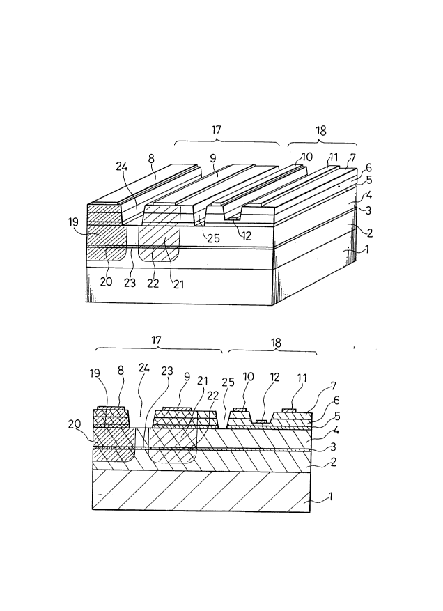
Figures l(a) and l(b) are a perspective view and a
cross-sectional view showing a long wavelength transmitter
OEIC in accordance with an emboA;ment of the present
invention;
Figures 2(a) to 2(f) are cross-sectional views showing
a method for manufacturing the long wavelength transmitter
OEIC of figure 1;
Figure 3 is a cross-sectional view showing a long
wavelength transmitter OEIC in accordance with the prior
art; and
Figures 4(a) to 4(i) are cross-sectional views showing
a method for manufacturing the long wavelength transmitter
OEIC of figure 3.
An embodiment of the present invention will be
described in detail with reference to the drawings.
Figures l(a) and l(b) are a perspective view and a
cross-sectional view showing a long wavelength transmitter
OEIC in accordance with an embodiment of the present
invention. In these figures, a semiconductor laser 17 and a
HEMT 18 are integrated on a semi-insulating InP substrate 1.
A lower AlGaInAs cladding layer 2 of the semiconductor laser
_ - 8 - 205~453
is disposed on the substrate 1. A quantum well active layer
3 comprising, for example, an AlGaInAs or AlInAs barrier
layer and an InGaAs well layer is disposed on the lower
cl~ i n~ layer 2. A high resistivity AlGaInAs clA~; ng
layer 4 is disposed on the quantum well active layer 3. An
undoped InGaAs operating layer 5 of the HEMT is disposed on
the upper cladding layer 4. An n type AlInAs carrier
supplying layer 6 is disposed on the operating layer 5. An
n type InGaAs contact layer 7 is disposed on the carrier
10 supplying layer 6. A p type dopant diffused region 19 and
an n type dopant diffused region 21 of the semiconductor
laser are opposed to each other at a predetermined interval
and penetrate through the layers from the contact layer 7 to
the quantum well active layer 3 to reach into the lower
15 cladding layer 2. A p side electrode 8 of the semiconductor
laser is disposed on the contact layer 7 in the p type
dopant diffused region l9~and a n side electrode 9
is disposed on the contact layer 7 in the n type region 21.
A gate electrode 12 of the HEMT is disposed on the bottom of
20 the recess groove penetrating the contact layer 7 and
reA~-h;ng into the carrier supplying layer 6. Source and
drain electrodes 10 and 11 of the HEMT are disposed on the
contact layer 7. Regions 20 and 22 of the quantum well
active layer 3 are disordered by diffusions of p type and n
25 type dopants, respectively. An active region 23 of the
- 9 - 205 1 453
semiconductor laser is sandwiched by the disordered regions
20 and 22. The p type region 19 and the n type region 21 of
the semiconductor laser are separated by the groove 24~and
the semiconductor laser 17 and the HEMT 18 are separated by
5 the y oove 25.
Figures 2(a) to 2(f) illustrate a method for
manufacturing the transmitter OEIC of figure 1.
On a semi-insulating InP substrate 1 shown in figure
2(a), an AlGaInAs lower cl~ing layer 2, a quantum well
10 active layer 3 comprising AlGaInAs or AlInAs barrier layer
and InGaAs well layer, a high resistivity AlGaInAs upper
cl~;ng layer 4, an undoped InGaAs operating layer 5, a n
type AlInAs carrier supplying layer 6 and a n type InGaAs
contact layer 7 are successively grown by MOCVD as shown in
figure 2(b). Then, as shown in figure 2(c), a p type dopant
such as Zn is diffused or bombarded from the surface of the
growth layer to form a p type region 19. The p type dopant
disorders the quantum well structure of the quantum well
active layer 3, resulting in region 20. Then, as shown in
20 figure 2(d), a n type dopant such as Si is diffused or
bombarded from the surface at a predeterm;ne~ interval from
the p type region 19 to form an n type region 21. The n
type dopant disorders the quantum well structure of quantum
well active layer 3, resulting in region 22. Then, as shown
25 in figure 2(e), a recess groove of the HEMT is formed by
C
` _ - lO - 205 1 453
etching and then a gate electrode 12 is formed on the bottom
of the recess groove. Then, as shown in figure 2(f), a
groove 24 for separating the p type region 19 from the n
type region 21 and a groove 25 for separating the
5 semiconductor laser 17 from the HEMT 18 are formed by
etching. Finally, p side and n side electrodes 8 and 9 of
the semiconductor laser and source/drain electrodes 10 and
11 of the HEMT are formed, completing a transmitter OEIC.
Description is given of the operation hereinafter.
Operation of the semiconductor laser 17 will be
described first. ~n the semiconductor laser 17, since n
type dopant such as Si and p type dopant such as Zn are
diffused from the surface of the epitaxy layers, the quantum
well active layer 3 is disordered in the respective dopant
15 diffused regions, resulting in the disordered regions 20 and
22 each having a larger effective energy band gap and
smaller refractive index than those of the non-diffused
region. When a positive voltage is applied to the p side
electrode 8 and a negative voltage is applied to the n side
20 electrode 9, a current flows only through the active layer
23 in the transverse direction because the upper and lower
cladding layers 2 and 4 have high resistivity. Then, holes
are injected into active region 23 from the disordered re-
gion 20, electrons are injected into active region 23 from
25 the disordered region 22, and the holes and electrons are
205 1 453
recombined to generate a light. When the current level is
increased, induced emission takes place and then laser
oscillation occurs. When the construction of the quantum
well layer 3, i.e., the thickness of InGaAs well layer and
5 the value of effective energy band gap of AlGa}nAs barrier
layer are appropriately established, the oscillation
wavelength can be set within a long wavelength region of 1.3
to 1.55 micron in which the absorption loss due to optical
fiber is small. Since the active region 23 is sandwiched by
10 the disordered regions 20 and 22 having small refractive
index, the light is confined in the direction parallel to
the active region 23. When the width of active region 23 is
set to approximately 2 microns or less, a flln~ental
transverse mode oscillation can be obtained.
Description is given of the operation of the HEMT 18
hereinafter. In the HEMT 18, the InGaAs operating layer 5
is disposed directly on the high resistivity AlGaInAs layer
4, i.e. on the cladding layer of the semiconductor laser 17.
For a HEMT it is necessary to provide a high resistivity
20 buffer layer beneath the operating layer to reduce the
leakage current. In the present invention, the high
resistivity cl~; ng layer of the semiconductor laser 17
also serves as the leakage current preventing layer of the
HEMT 18. The principle of operation of HEMT 18 is as same
25 as that of the conventional one. More specifically,
C
~ 12 -
2Q5 1 453
electrons are supplied from the AlInAs carrier-supplying
layer 6 to the InGaAs operating layer 5 having a low impurity
concentration (approximately 10l5 cm-3 or less) and less
impurity dispersion, and a two-dimensional electron gas is
5 generated at the interface between the operating layer 5 and
the carrier supplying layer 6. When the voltage applied to
the gate electrode 12 is varied, the level and shape of
potential in the vicinity of the interface between the
operating layer 5 and the carrier supplying layer 6 vary
10 accordingly, and the concentration of the two-~;r~nsional
electron gas also varies. That is, the current is subjected
to a modulation by the variation in the gate voltage.
The transmitter OEIC of the present invention, in which
the semiconductor laser 17 and the HEMT 18 are integrated on
15 a substrate 1, operates in a state that the n side electrode
9 of the semiconductor laser is connected with the source
electrode 10 of the HEMT by a wiring. Thus, the ~EMT 18
controls the operating current of semiconductor laser 17 and
gives signal modulations such as modulations of brightness
20 or strength of light output of the semiconductor laser 17.
As described above, in the present invention, a
transverse direction current injection type semiconductor
laser having a high resistivity upper cl~ing layer and a
HEMT having an operating layer on the high resistivity upper
25 cladding layer are integrated on a substrate. More
- 13 -
205 1 453
specifically, the semiconductor laser includes an AlGaInAs
lower cladding layer, a quantum well active layer and a high
resistivity AlGaInAs upper cl~ ng layer successively grown
on the substrate, disordered regions formed in the quantum
well active layer by diffusions of p type and n type
dopants, and an active region sandwiched by the disordered
regions. The HEMT includes an operating layer formed on the
high resistivity AlGaInAs upper cladding layer~and uses the
upper cladding layer as a leakage current preventing layer.
Therefore, it is not necessary to provide a special leakage
current preventing film for the HEMT. In addition, the
above structure can be formed by only one epitaxial growth.
As a result, the epitaxial process can be simplified and the
costs can be reduced. Furthermore, since the crystals for
the semiconductor laser and those for the HEMT are
successively grown on a flat substrate having no step
difference, photolithography can be performed on a flat
surface with no step difference in the later process for
forming a gate of HEMT, so that a gate pattern of 1 micron
or less can be easily formed at high precision. As a
result, a transmitter OEIC performing high speed modulation
can be realized. In addition, since AlGaInAs series
material is used in the present invention, the oscillation
wavelength of the semiconductor laser can be set within a
long wavelength region of 1.3 to 1.55 micron in which the
C
- 14 -
2051453
absorption loss due to transmitter optical fiber is small,
and a high speed HEMT can be constituted. In addition, such
a long wavelength semiconductor laser of 1.3 to 1.55 micron
band and originally high speed InGaAs/AlInAs series HEMT can
5 be easily integrated on an InP substrate, resulting in
be easily integrated on an InP substrate, resulting in a
higher-speed transmitter OEIC.
$