Note: Descriptions are shown in the official language in which they were submitted.
2~5~.'~6q~.
METHOD AND APPARATUS FOR FORMING ELECTROPHOTOGRAPHIC IMAGE
BACKGROUND OF THE INVENTION
This invention relates to a method and an apparatus for
forming an image b;y utilizing electrophotography and, more
particularly, to a method and an apparatus for forming an
electrophotographic image without using corona discharge
means.
A conventional image forming method using corona
discharge means includes the steps of uniformly charging a
surface of a sensitive medium by a corona discharge means to
set a predetermined polarity, exposing the charged surface
of the sensitive medium to a light image to selectively
disperse the charges on the sensitive medium so that an
electrostatic latent image is formed, supplying toner to the
surface of the sensitive medium by a development sleeve to
which a suitable bias is applied so that the electrostatic
latent image formed on the sensitive medium is developed,
and transferring the developed toner image on the sensitive
medium onto a receptor sheet by using transfer corona
discharge means.
This conventional method entails the problem of an
offensive smell of ozone generated by corona discharge and
the problem of a toxicity of ozone to the human body. This
method also entails the problem of the quality of a formed
- 1 -
~~~.'~~~c
copied image being easily influenced by environmental
conditions, i.e., humidity, existence of dust, and other
factors.
For the purpose of solving these problems, an image
forming method has been proposed in which a charging roller
or a transfer roller to which an external voltage is applied
is used instead of corona discharge means.
In a known method of this kind, an electroconductive
base of a sensitive medium is grounded, and a charging
roller to which a DC bias voltage is applied is brought into
contact with a surface of the sensitive medium to charge the
surface of the sensitive medium. Then the surface of, the
sensitive medium i.s exposed to a light image of an original
to be copied, and an electrostatic image corresponding to
the original image is thereby formed on the sensitive
medium. The electrostatic image is developed by toner
carried by a deve7_opment sleeve connected to a suitable bias
supply. The deve7.oped toner image is transferred onto a
receptor sheet such as a paper sheet by a transfer roller to
which a transfer bias voltage is applied. The developing
powder remaining on the surface of the sensitive medium
after transfer is removed from the surface by a cleaning
brush to which a suitable cleaning bias is applied.
This method c:an solve the above-mentioned problems of
ozone. In this mE~thod, however, it is difficult to charge
:~51'p6~-
the sensitive medium surface uniformly and there is a
potential problem of image unevenness or background fog of
the resulting copied image.
For the purpose of solving this problem, a method of
applying a pulsating voltage to the charging roller has been
proposed as disclosed in Japanese Laid-Open Patent
application No.63-149668, for example.
This conventi~~nal method enables a reduction in charge
unevenness on the sensitive medium surface but does not
enable a reduction in the overall size of the apparatus.
This method requires high-voltage power sources for units of
image forming means, i.e., a power source for the charging
roller, a power sovurce for the development bias, a power
source for the transfer roller and a power source for the
cleaning bias. Fo.r this reason, if this method is used, it
is difficult to pr~wide a low-cost compact image forming
apparatus.
SUMMARY OF THE INVENTION
It is therefore an object of the present invention to
provide a novel image forming method which minimizes the
number of power sources for image forming means to reduce
the size and the price of the apparatus.
Another object of the present invention is to provide
an image forming method enabling to reproduce a clear image
free from image unevenness and background fog, and an
_ 3 _
2051764
apparatus based on this method. _
Still another object of the present invention is to
provide an image forming apparatus using no corona discharge
means and reduced in its size.
A further object of the present invention is to
provide an image forming apparatus having a development means
for providing a necessary development bias on a developer
supply member without using an additional bias supply.
A still further object of the present invention is to
provide a simple construction of a transfer member arranged to
improve transfer efficiency without using an additional bias
supply.
To achieve these and other object, according to one
aspect of the prESSent invention, there is provided an image
forming method comprising the steps of:
applying an alternating current voltage or a
voltage obtained by superposing a direct current voltage on an
alternating current voltage to an electroconductive base of a
photosensitive medium having a photoconductive layer formed on
the electroconduct:ive base, the photosensitive medium being for
receiving an electrostatic image formed on the photoconductive
layer;
bringing a grounded electroconductive or semi-
electroconductive member into contact with or close to a
surface of the photosensitive medium to charge the surface to
a predetermined polarity; and
exposing the surface of the photosensitive
medium to a light image to form the electrostatic image.
As the grounded electroconductive or semi-electro-
conductive member is brought into contact with or
4
2o5~~s4
close to the surfac~° of the electroconductive base of the
sensitive medium to which the bias voltage is applied,
charges~of the predetermined polarity are induced on the
photoconductive layer surface of the sensitive medium in
accordance with the bias voltage, thereby charging the
sensitive medium surface. The surface of the sensitive
medium is then exposed to a light image to form on the
sensitive medium surface an electrostatic image
corresponding to the exposure image.
According to another aspect of the present invention, a
developer supplier for developing the electrostatic image is
grounded directly or through an induced bias means, and
charges are induced on the developer supplier by the bias
voltage applied to the electroconductive base of the
sensitive medium, thereby establishing a necessary
development bias. The voltage of the development bias is
set according to the rating value of the induced bias means
connected to the developer supplier.
According to still another aspect of the invention, an
alternating current voltage or a voltage obtained by
superposing a direct current voltage on an alternating
current voltage generally in phase with the voltage applied
to the electroconductive base of the sensitive medium is
applied to a transfer member. Specifically, this voltage
applied to the transfer member is supplied from the power
2051764
source for applying the bias voltage to the electroconductive
base of the sensitive medium.
According to the present invention, there is also
provided an image forming method comprising the steps of:
applying a direct current voltage to an electro-
conductive base of a photosensitive medium, the photosensitive
medium being for receiving an electrostatic image thereon;
bringing a grounded electroconductive or semi-
electroconductive member into contact with or close to a
surface of the photosensitive medium to charge the surface to
a predetermined polarity; and
exposing the surface of the photosensitive medium to
a light image to form the electrostatic image.
The present invention further provides an image
forming apparatus comprising:
a photosensitive drum having at least an
electroconductive :base and a photoconductive layer for forming
an electrostatic image thereon;
means far applying an alternating current voltage or
a voltage obtained by superposing a direct current voltage on
an alternating current voltage to the electro-conductive base
of said sensitive drum;
an elect:roconductive or semi-electroconductive member
disposed into contact with or close to a surface of said
photosensitive drum and grounded;
means fc>r exposing the surface of said photosensitive
drum to a light image; and
a developer supplier disposed close to the surface of
said photosensitive drum and grounded directly or through
induced bias mean; .
These and other objects, features and advantages of
the present invention will become clear for those skilled in
the art from the following description of preferred embodiments
taken in conjunction with the accompanying drawings.
6
1
2051764
BRIEF DESCRIPTION OF THE DRAWINGS
Fig. 1 :is a schematic diagram of an example of an
image forming apparatus in accordance with the present
invention in which a voltage obtained by superposing a direct
current on an alternating current is applied to an
electroconductive base of a sensitive medium;
Fig. 2 is an equivalent circuit diagram relating to
the sensitive medium and an induced member in accordance with
the present invention;
Fig. 3 is a graph showing changes in the surface
potential of the sensitive medium when a positive bias voltage
is applied to thE~ sensitive medium having an N-type photo-
conductive layer i.n accordance with the present invention;
Fig. 4 is a diagram of waveforms of the surface
potential of the :sensitive medium;
Fig. 5 is a schematic diagram of another example of
the image forming apparatus in accordance with the present
invention in which an alternating current voltage is applied
6a
A
2051764
y
to the electroconductive base of the sensitive medium;
Fig. 6 is a schematic diagram of still another example
of the image forming apparatus in accordance with the
present invention in which a direct current voltage is
applied to the electroconductive base of the sensitive
medium;
Fig. 7 is a schematic diagram of an arrangement for
producing an induced bias on the transfer roller;
Fig. 8 is a schematic diagram of an arrangement in
which the bias supply for the sensitive medium also serves
as a bias supply for the transfer roller;
Fig. 9 is a diagram of an example of the bias supply
shown in Fig. 8; and
Fig. 10 is a schematic diagram of an arrangement in
which an alternating current bias supply for the sensitive
medium also serves as a bias supply for the transfer
roller.
DESCRIPTION OF THE PREFERRED EMBODIMENTS
A method and an apparatus for forming images in
accordance with the present invention will be described
below with reference to the accompanying drawings.
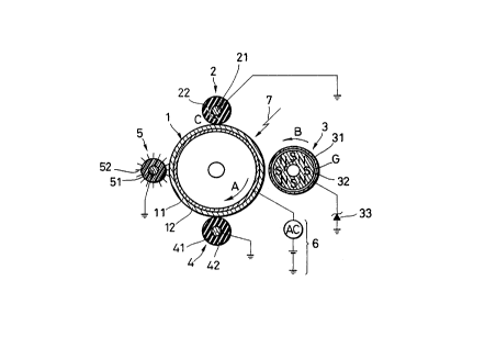
Fig. 1 shows an example of an image forming apparatus
based on a method in accordance with the present invention.
A sensitive medium. 1 includes a drum-like electroconductive
base (which may comprise a drum formed of an insulating
2051764
material and an ele~~troconductive layer formed on the drum)
11, and a photoconductive layer 12 formed on the surface of
the base 11 by bein~~ deposited or applied thereto. As the
material of the pho~toconductive layer 12, any of
photoconductors of l?- or N-type, e.g., OPC, Se, ZnO, CdS,
and a-Si can suitably be used. An insulating layer may be
formed on the photo~~onductive layer 12. The base 11 of the
sensitive medium 1 .is electrically connected to a bias
supply 6. In this example, the bias supply 6 applies to the
base 11 a voltage which is obtained by superposing a DC
voltage on an AC voltage. The frequency of the AC voltage
is, preferably, in tithe range of 80 Hz to 30 kHz, more ;
preferably, in the :range of 150 Hz to 3 kHz. Preferably,
the superposed DC voltage is positive with respect to an N-
type photoconductor, or is negative with respect to P-type
photoconductor., Th~3 bias 6 may be an AC voltage or DC
voltage alone as described later, although a voltage
obtained by superposing a DC voltage on an AC voltage
enables uniform charging most preferably.
The sensitive medium 1 is connected to a suitable drive
means and is rotated in the direction of arrow A during
operation.
A member 2 is ~9isposed in contact with or close to the
surface of the sensitive medium 1. The member 2 has the
shape of a roller and has a construction in which a layer 22
CA 02051764 1999-09-23
J
of an electroconductive elastic rubber material is formed
on the circumferential surface of an electroconductive
metallic core 21 rotatably supported. In the illustration,
the member 2 is shown in a state of contacting the surface
of the sensitive medium 1. Alternatively, the member 2 may
be disposed close to the sensitive medium 1 so that a small
air gap (preferably, 120 ~m or less) is formed between the
member 2 and the surface of the sensitive medium 1. In
either case, i.e., in the contact or close position, the
member 2 is preferably rotated in a direction (indicated by
arrow C) corresponding to the direction of rotation of the
sensitive medium 1 at the same peripheral speed as the
sensitive medium 1. It has experimentally been found that
if the member 2 is not rotated, charge unevenness occurs in
some cases . The member 2 can be rotated by being connected
an independent drive source or by receiving a torque of the
sensitive medium 1 through a suitable drive transmission
means such as a gear train.
The layer 22 may be formed by dispersing an
electroconductive powder in an elastic material such as
nitrile rubber (NBR), urethane rubber or silicon rubber. A
dielectric layer 23 formed of a synthetic resin such as a
silicone resin or a polyethylene resin may be formed on the
outer circumferential surface of the layer 22. (Examples of
such a construction are illustrated in Figs. 5 and 10). The
r
9
2491764
layer 22 may be a semi-electroconductive material (having a
resistivity of, for example, 105 to 101 S2cm, for example) as
well as an elastic electroconductive material (having a
resistivity of, for example, smaller than 105 S2cm). The
member 2 may alternatively be a rigid metallic member having
no elastic layer. The core 21 is grounded directly or
through a rectifier means 8 (Fig. 5) or induced bias means
such as a varistor, a constant-voltage diode or an ordinary
diode. To obtain a desired voltage on the surface of the
sensitive medium, an arrangement such that the core 21 is
grounded through a suitable resistor may suffice. The shape
of the member 2 is, most preferably, such that a surface
gradually spaced apart from the surface of the sensitive
medium 1 is formed, as in the case of a roller. However,
the member 2 may alternatively have the shape of a blade or
a brush.
Fig. 2 is an equivalent circuit diagram of a circuit
for charging the surface of the sensitive medium 1. Under a
dark condition, a predetermined bias voltage which is an AC
voltage or a voltage obtained by superposing a DC voltage on
an AC voltage is applied to the base 11 of the sensitive
medium 1 by the power supply 6, and the member 2 is brought
into contact with c~r close to the surface of the sensitive
medium. Then the voltage is divided in accordance with the
impedances of the sensitive medium 1, the member 2 and the
- 10 -
2051764
air layer therebet.ween, and the charge in accordance with
the corresponding divided value is induced on the surface of
the sensitive medium 1.
Fig. 3 schematically shows changes in the surface
potential of the :sensitive medium 1 in a case where a bias
voltage obtained by superposing DC and AC voltages so that
the voltage is sh9_fted to the positive side is applied to
the base 11 of the sensitive medium 1 having N-type
photoconductive layer 12 under a dark condition. A negative
charge is induced on the surface of the sensitive medium 1
in contact with the member 2 and the voltage is reduced to
the divided value, as described above. The surface o.,f the
sensitive medium 7. is then exposed to a light image to be
copied by an optical means such as a laser or an LED. The
surface potential (VL) at a position (exposed region)
corresponding to a bright portion of the image thereby
becomes closer to the bias voltage applied to the base 11 of
the sensitive med~.um 1, thereby creating a potential
difference from the voltage (VD) at a position (non-exposed
region) corresponding to a dark portion of the image. In
the image forming method in accordance with the present
invention, therefo re, an electrostatic image is formed such
that the potentia=L corresponding to a bright image portion
is higher while the potential corresponding to a dark image
portion is lower, which relationship is reverse to that in
- 1 1 -
2051764 a
the conventional method using corona discharge. In Fig. 3,
the bright potential and the dark potential are indicated by
straight lines for convenience. Actually, however, the
surface potential of the sensitive medium 1 oscillates by
superposition of the AC bias voltage applied to the base 11.
Fig. 4 shows t:he dark potential and the bright
potential on the surface of the sensitive medium 1 in a case
where a bias voltage obtained by superposing an AC voltage
of 1,500 Vp-p at a frequency of 4 kHz on a DC voltage of +
400 V is applied to the base 11 of the sensitive medium 1,
and where the surface of the sensitive medium 1 is
irradiated with li<~ht image to form an electrostatic latent
image. The waveform of the amplitude is generally equal to
the waveform of thE: bias voltage applied to the base 11 of
the sensitive medium 1, and the frequency is generally equal
to that of the bias voltage.
When a negati~ae voltage is applied to the base 11 of
the sensitive medium having a P-type photoconductive layer,
a positive load is induced on the surface of the sensitive
medium l, as in th<~ above .
Referring back to Fig. 1, the electrostatic image
formed on the sensitive medium is developed by a development
means 3. The deve:Lopment means 3 includes an
electroconductive ;sleeve 31 disposed close to the surface of
the sensitive medium 1, and a magnet roller 32 disposed
_ 1 ? _
2051764v
inside the sleeve 31 with a space G formed therebetween.
The sleeve 31 and the magnet roller 32 are provided so as to
be rotatable independently of each other at different
speeds. In this example, the sleeve 31 and the magnet
roller 32 rotate respectively in a direction (indicated by
arrow B) opposite to the direction of rotation of the
sensitive medium 1. These members are rotated by a drive
source and a transmission means, such as a gear train, which
are known per se. As is well known, a developer contained
in a developer casing is attracted by the magnetic force of
the magnet roller 32 to form a magnetic brush on the surface
of the sleeve 31, although this magnetic brush is not;
illustrated. The thickness of the magnetic brush is made
uniform by a doctor blade which is known per se. The
developer is tran~;ported in the direction of arrow B at a
speed generally edual to or slightly smaller than the
peripheral speed of the sensitive medium 1, in contact with
or close to the surface of the sensitive medium 1, and
develops the electrostatic image to form a toner image. As
the developer, a one-component magnetic toner or a two-
component developE~r formed of a toner and a magnetic
carrier.
The sleeve 3.L is grounded directly or through an
induced bias means 33 such as a constant-voltage diode, a
high-resistance rESSistor or a varistor. In the example
_ i 3 _
2051764
shown in Fig. 1, the sleeve 31 is grounded through induced
bias means 33, and a predetermined development bias is
induced on the sleeve 31 by the voltage applied to the base
11 of the sensitive medium 1. Development is effected under
this development bias and the AC bias applied to the base
11. The bias voltage of the sleeve 31 depends upon the
rating value of induced bias means 33 such as a constant-
voltage diode or a varistor connected to the sleeve 31. For
example, for a digital printer using reversal development,
induced bias means 33 having a rating value such that the
potential of the sleeve 31 is closer to the dark potential
of the sensitive medium is selected.
The AC electric field applied to the base 11 of the
sensitive medium 1 makes the developer between the sensitive
medium 1 and the sleeve 31 oscillate to move reciprocatively
so that the electrostatic image is clearly developed.
The toner image formed on the sensitive medium 1 is
transferred onto a receptor sheet such as a paper sheet by a
transfer means 4. The transfer mean 4 has a roller
structure which is generally the same as that of the member
2, and includes a grounded electroconductive metallic core
41 and an electroccnductive or semi-conductive layer 42 laid
on the metallic core 41 and having a resistivity of 103 to
101 S2cm. A dielectric layer 43 (Figs. 5 and 10) may also
be provided on the layer 42. The transfer means 4 is
- 14 -
20 517 fi 4~
disposed in contact with or close to the sensitive medium 1,
a transfer bias having a polarity opposite to that of the
toner image is induced by the bias voltage applied to the
base 11 of the sensitive medium 1, and the toner image on
the sensitive medium is transferred onto the transfer member
under this transfer bias. The transfer means 9 may
alternatively have the shape of a pad or belt.
The toner remaining on the surface of the sensitive
medium 1 after transfer is removed to clean the surface by a
cleaning means 5, so that the sensitive medium 1 is ready
for next image formation. The cleaning means 5 is formed
of, for example, a cleaning brush having an
electroconductive core 51 and an electroconductive brush 52
embedded in the core 51. The core 51 is grounded directly
or through a constant-voltage diode, a varistor or the like.
The residual toner on the sensitive medium 1 is thereby
attracted or moved electrostatically and physically by the
brush 52 to be removed from the sensitive medium 1. The
toner attached to the brush 52 is removed by a scraper (not
shown) disposed so as to be capable of contacting the brush
52. Instead of the brush 52, a biased cleaning roller may
be used. After cleaning, the surface of the sensitive
medium 1 is discharged by an eraser lamp (not shown), if
necessary.
Fig. 5 shows a case where the bias voltage applied to
- 1 5 -
20517fi~:
the base 11 of the sensitive medium 1 consists of an AC
voltage alone (no I)C voltage is superposed). In this case,
the member 2 and the transfer roller 4 are grounded through
rectifier means 8 and 44, respectively. The member 2 and
the transfer rolle~_ 4 are covered with dielectric layers 23
and 43, respectively. The arrangement is the same as that
shown in Fig. 1 in other respects. In Fig. 5, the
components identical or corresponding to those shown in Fig.
1 are indicated by the same reference characters.
Fig. 6 shows ~~ case where the bias voltage applied to
the case 11 of the sensitive medium 1 is a DC voltage. In
this case, the biaa voltage is set to positive polarity with
respect to an N-type sensitive medium, or to negative
polarity with respect to a P-type sensitive medium. The
arrangement is the same as that shown in Fig. 1 in other
respects, and the name components are indicated by the same
reference characters.
The bias voltage applied to the base 11 of the
sensitive medium 1 is, preferably, a voltage obtained by
superposing an AC 'voltage on a DC voltage. However, using
an AC or DC voltage alone as in the arrangement shown in
Fig. 5 or 6 is not excluded from the scope of the present
invention.
Fig. 7 shows .another example of the transfer means 4.
In this example, t:he core 41 is grounded through induced
- 16 -
2051764
bias means 44 such as a diode, and the sleeve 31 of the
development means 3 is grounded through a varistor 33. The
member 2 is grounded through rectifier means 8. The
arrangement is the same as that shown in Fig. 1 in other
respects.
The transfer means 9 transfers the toner image by a
transfer bias induced by the diode 94. The direction of
connection of the diode 44 is determined by the kind of
development. For example, transfer in the case of reversal
development using an N-type sensitive medium is as described
below. A voltage is applied to the base 11 of the sensitive
medium 1 by superposing an alternating current on a direct
current biased to positive polarity, and the member 2 is
grounded through a diode 8, a cathode of the diode 8 being
connected to ground. The potential of the electrostatic
image formed on thE~ sensitive medium 1 is positive. In this
case the electrostatic image is developed by a toner of
negative polarity. The transfer means 4 is therefore
arranged to producE: a positive transfer bias. The diode 44
is grounded by being connected at its anode to ground. A
positive half-wave voltage is induced on the transfer means
4, and the toner irnage is transferred under this transfer
bias. The arrangernent is substantially the same in a case
where only an AC b_Las is applied to the base 11 of the
sensitive medium 1.,
_. 2051764
Figs. 8 and 1C~ show examples of an arrangement in which
the transfer means 4 is connected to the bias supply 6.
Components identical or corresponding to those shown in Fig.
1 or 5 are indicated by the same reference characters.
Referring to F'ig. 8, a voltage obtained by superposing
an alternating current on a direct current is applied to the
base 11 of the sen~~itive medium 1 by the bias supply 6. The
core 41 of the transfer means 4 is connected to an output
terminal of the bias supply 6, and a voltage of an
alternating current. or a current obtained by superposing a
direct current on am alternating current which voltage is
generally in phase with the bias voltage applied to the base
11 of the sensitive medium 1 is applied to the core 41. In
several experiment;, occurrence of blur in a copied image
due to an increase in the voltage between the transfer means
4 and the sensitive medium 1 was observed in a case where
only a DC voltage Haas applied to the core 41. With respect
to the case of applying only an alternating current to the
core 91, as well, occurrence of blur in a copied image or
damage to the image was observed when there was a phase
difference between the alternating current applied to the
core 41 and the alternating current applied to the sensitive
medium 1. In contrast, no blur was recognized in the case
of the above arrangements.
Fig. 9 shows an example of the bias supply 6 of the
- 1 f~ -
2051764
arrangement shown in Fig. 8. A tap of a different output
level is provided c>n the output coil of the bias supply 6 to
apply a transfer bias to the transfer means in accordance
with a predetermined condition for the image formation
process. As mentioned above, this voltage has an amplitude
generally in phase with the bias voltage applied to the base
11 of the sensitive medium 1.
Referring them to Fig. 10, the bias voltage to the base
11 of the sensitive medium 1 has an AC component alone, and
the core 41 of the transfer means 4 is connected to an
output terminal of the bias supply 6 through diode 44. In
this example, the r>ias supply 6 has an AC component alpne
but a DC component may also be superposed thereon.
Experimental Examp7.e 11
In an apparatus arranged as shown in Fig. 1, a voltage
obtained by superposing a DC voltage of + 1,100 V on an AC
voltage of 1,500 V~>-p at a frequency of 2 kHz was applied to
base 11 of sensitive medium 1 having N-type organic
photoconductive la~~er 12, and sensitive medium 1 was rotated
in the direction of: arrow A at a peripheral speed of 40
mm/sec. Member 2 raving grounded core 21 and elastic layer
22 formed of NBR, Urethane or a silicone rubber and an
electroconductive ~>owder mixed in the rubber was brought
into contact with t:he surface of sensitive medium 1 under a
dark condition, anti the sensitive medium surface was
- 19 -
2051764:
irradiated with la:;er light 7 to form an electrostatic
image. At this time the surface potential of the sensitive
medium was measured. The dark potential of the
electrostatic image was + 280 V while the bright potential
was + 1,050 V. Then the electrostatic image was developed
by a one-component magnetic toner of positive polarity and
by using development sleeve 31 grounded through a constant-
voltage diode having a rating of 760 V. As development
sleeve 31, a sleev~s having an outside diameter of 18 mm,
formed of SUS 309 ,and having its surface processed by
shotblast of about 400 mesh was used. Magnetic roller 32
having six magneti~~ poles S and N alternately disposed was
rotated in development sleeve 31 so that an alternating
magnetic field of ,about 600 gauss at the surface of sleeve
31 was applied to the toner. The distance between sensitive
medium 1 and devel~~pment sleeve 31 was 0.3 mm. The toner on
development sleeve 31 is brought into contact with the
surface of sensitive medium 1 to effect development. The
toner image thereby developed was transferred onto a
transfer sheet by transfer means 4 and was fixed, thereby
obtaining a clear ~~opied image free from fog.
Ex~?erimental Example 2
Experiment was made in such a manner that the frequency
of the AC component of the bias voltage applied to base 11
of sensitive medium 1 was changed in the range of 80 to 30
- 20 -
2051764.;
kHz, and that other conditions were the same as those for
Example 1. A clear copied image was thereby formed.
Experimental Exam,~le 3
Experiment waa made in such a manner that only an AC
voltage was used as the bias voltage applied to base 11 of
sensitive medium 1,, member 2 and the transfer roller 4 were
grounded through rectifier means 8 and 49, respectively, and
other conditions were the same as those for Example 1. A
clear copied image was thereby formed.
Experimental Exam~Le 4
Development w~3s effected by using a two-component
developer formed o:E a mixture of a magnetic toner and;5 to
95 ~ by weight of .3 carrier was used under the same
conditions as Exam~~le 1. A clear image was thereby
obtained. 25 to 6.5 o by weight of a ferrite powder was
contained in the magnetic toner used.
Experimental Example 5
In an apparatus arranged as shown in Fig. 6, a DC
voltage of + 1,100 V was applied to base 11 of sensitive
medium 1 having N-type organic photoconductive layer 12, and
sensitive medium 1 was rotated in the direction of arrow A
at a peripheral speed of 40 mm/sec. Member 2 having
grounded core 21 a:nd elastic layer 22 formed of NBR,
urethane or a silicone rubber and an electroconductive
powder mixed in the rubber was brought into contact with
- 21 -
2051764:
sensitive medium 1 under a dark condition, and the sensitive
medium was irradiated with laser light 7 to form an
electrostatic image. At this time the surface potential of
the sensitive medium was measured. The dark potential of
the light image was + 550 V while the bright potential was +
1,050 V. Next, the electrostatic image was developed by
contact with a one-component magnetic toner of positive
polarity and by using development sleeve 31 grounded through
a constant-voltage diode of 760 V. A clear copied image was
thereby obtained.
Experimental Examplgs
In an apparatus arranged as shown in Fig. 6, a DC;
voltage of - 1,100 V was applied to base 11 of sensitive
medium 1 having P-type organic photoconductive layer 12, and
an electrostatic irr~age was formed in substantially the same
manner as Example 5 and was developed by a one-component
magnetic toner of negative polarity. A clear copied image
was thereby obtained.
Experimental Example 7
Experiment was. made by using the two-component
developer used in Example 4 while other conditions were the
same as those for Example 5. A clear copied image was
thereby obtained.
Experimental Example 8
Experiment was. made by using the two-component
- 22 -
2051764 .
developer used in Example 4 (but toner polarity is negative)
while other conditions were the same as those for Example 6.
A clear copied image was thereby obtained.
Experimental Example 9
In an apparatus arranged as shown in Fig. 7, a voltage
obtained by superposing an AC voltage of 1,500 Vp-p (at a
frequency of 80 Hz to 30 kHz) on a DC voltage of + 400 V was
applied to base 11 of sensitive medium 1 having N-type
organic photoconductive layer 12, and sensitive medium 1 was
rotated in the direction of arrow A at a peripheral speed of
40 mm/sec. Member 2 having elastic layer 22 formed of NBR
or a silicone rubber and an electroconductive powder mixed
in the rubber was brought into contact with sensitive medium
1 under a dark condition, and the sensitive medium was
irradiated with laser light 7 to form an electrostatic
image. This image was developed by reversal development.
For the development, a two-component developer having a
resistivity of about 10~ to 109 S2cm and formed of a mixture
of 100 ~ by weight of a spherical ferrite carrier having an
average particle size of 50 ~.m and 5 ~ by weight of a toner
containing an acrylic resin as a main component was used.
As development sleeve 31, a sleeve having an outside
diameter of 18 mm, formed of SUS 304 and having its surface
processed by shotblast of about 400 mesh was used and was
connected to a DC bias supply. Magnetic roller 32 having
- 23 -
2051764:
six magnetic poles S and N alternately disposed was rotated
in development sleeve 31 so that an alternating magnetic
field of about 600 gauss at the surface of sleeve 31 was
applied to the toner. The distance between sensitive medium
1 and development sleeve 31 was 0.3 mm. The toner on
development sleeve 31 is brought into contact with the
surface of sensitive medium 1 to effect development. The
developed image was transferred onto a transfer sheet by
transfer means 4 grounded through diode 44, thereby
obtaining a clear image free from background contamination.
The similar result was obtained in case of grounding
the development sleeve through a varistor.
Experimental Example 10
Experiment was made by using a one-component magnetic
toner having an average particle size of 12 ~tm and a
resistivity of 1014 to 1015 S2cm while other conditions were
the same as those for Example 9. A clear image free from
background contamination was thereby obtained.
experimental Example 11_
Experiment was made in such a manner that 6 g of a
spherical ferrite powder of 35 to 60 ~Lm was previously
attached uniformly to the development sleeve surface as a
developer carrier, the toner had an average particle size of
12 ~t.m and a resistivity of 1014 to 1015 S2cm, and other
conditions were th.e same as those for Example 9. A clear
- 24 -
2051764
image free from background contamination was thereby
obtained.
Experimental Example 12
In an apparatus arranged as shown in Fig. 8, a toner
image was formed under the same conditions as Example 9.
The toner image was transferred by transfer roller 4
connected power supply 6 as shown in Fig. 9. A clear image
free from background contamination was thereby obtained.
Experimental Exampl 1
Experiment was made by using a one-component magnetic
toner having an average particle size of 12 dim and a
resistivity of 1019 to 1015 S2cm while other conditions were
the same as those for Example 12. A clear image free from
background contamination was thereby obtained.
experimental Example 14
Experiment was made in such a manner that 6 g of a
spherical ferrite powder of 35 to 60 ~.Lm was previously
attached uniformly to the surface of development sleeve 31
as a developer carrier, the toner had an average particle
size of 12 dim and a resistivity of 1019 to 1015 S2cm, and
other conditions were the same as those for Example 12. A
clear image free from background contamination was thereby
obtained.
According to the present invention, as described above,
a means for applying a bias voltage to the base 11 of the
- 25 -
205~~s4
sensitive medium 1 is used and the need for charging means
and expensive high--voltage power sources for the development
sleeve, the transfer roller and so on is eliminated, thereby
making it possible to provide a simple and low-cost image
forming apparatus.
An alternating current or an alternating current on
which a DC current is superposed is used, whereby a clear
image free from foci, in particular, can be obtained. It is
also possible to induce charge for the cleaning brush in the
same manner without. praviding any additional power source.
The apparatus can l:hereby be simplified.
In the embodirnents shown in Figs. 8 and 10, the voltage
applied to the transfer roller and the voltage applied to
the sensitive medium are generally in phase with each other.
It is thereby possible to prevent. occurrence of an abnormal
voltage between th~~ sensitive medium and the transfer roller
and, hence, to form an image free from blur.
- ?6 -