Note: Descriptions are shown in the official language in which they were submitted.
2 ~ 3 2
Power supply device
The invention relates to a power supply device, particularly
suitable for supplying power to a filament of a transmltter tube,
provided with a filament transformer, a pulse transformer and
terminals for an AC generator, ~here a secondary side of the
filament transformer is coupled with the filament, a primary side of
the ~ilament transfor~er is coupled with the terminals and where a
secondary side of the pulse transformer is coupled with th~
filament.
Such a davice can be applied in a radar transmitter for the
generation of radar transmit pulses. The radar transmitter will be
provided with a high-power radar transmitter tube, such as a
cross-field amplifier, a travelling wave tube or a klystron, whose
cathode is at a pùlsed high-voltage potential. A problem, howaver,
is posed by the filament, which forms the cathode or is contained in
the cathode and which must be supplied with a filament voltage.
Filament voltage is required to heat the cathode to a high
temperature, to ensure electron emission to a sufflcient degrae.
On the basis of a solution, known from the literature, it is
essential to the filament voltage transformer that the capacitance
between the primary and secondary winding is very small, since this
capacitance forms a parasitic load on the pulse transformer which
supplies the cathode of the radar transmitter tube with pulsed high
voltage. This type of transformer having a small capacitance between
the windings is known to possess a high leakage self-inductance, as
a result of which, in loaded condition, the output voltage among
other things depends on the frequency of the primary voltage and the
temperature of ~he transformer. As such this transformer is less
suitable for supplying a filament, whose voltage has been stipulated
by the manufacturer.
20~2~3~
The power supply device Pccording to the invention eliminates these
drawbacks and is characterised in that the secondary side of the
pulse transformer is coupled with the filament via a bifilar
winding, the power supply device belng furthermore provided with a
decoupling network through which the bifilar winding is earthed.
It is therefore possible to connect a voltmeter to the filament via
the bifilar winding, enabling the filament voltage to be
continuously monitored.
The use of bifilar winding for the secondary winding of a pulse
transformer, which supplies the radar transmitter tube with a pulsed
high vol~age, ls as such an established technique. The filament
voltage is connected between the two ends of the windings which
are substantially at earth potential and the filament of the radar
transmitter tube is connected between the two ends of the winding
which are at the pulsed high voltage.
A concomitant of this solution is that the hester current flows
through the secondary winding of the pulse transformer.
Consequently, additional provisions for the cooling of the secondary
filament will have to be made and extra thick wfre or foil for the
secondary winding will have to be selected. This renders the pulse
transformer less compact and increases the leakage self-inductance
of the pulse transformer. This leakage self-inductance determines
the actual quality of a pulse transformer, it restricts the possible
slope of the high-voltage pulse and the maximum possible
transformation ratio. The above power supply device according to the
invention does not have these drawbac~s.
The invention will now be described in more detail with reference
to the following figures, of which:
Fig. 1 represents a diagram of a state-of-the-art power supply
- device;
2 ~
Pig. 2 represents a diagram of an alternative state-of-the-art power
supply devlce;
Fig. 3 represents a diagram of a power supply device according to
the invention;
Fig. 4 represents a drawing of the filament voltage ~ransformer.
A state-of-the-art power supply device can be implemented In a radar
transmitter, as schematically represented in Fig. 1. of a radar
transmitter tu~e 1, only a filament 2 is illustrated; it may be
assumed that the other parts of the radar transmitter tube are
practically at earth potential. Pulse ~ransformer 3 is provided with
a primary winding 4, at the input terminals of which a pulse-shaped
voltage can be applied. A secondary winding 5 is a bifilar one. A
bifilar wlnding consists of two parallel current conductors instead
of a single one. One side of the winding 5 is, via a secondary
winding 7 of a filament voltage transformer 6, substantially at
earth potentlal. The other slde of the winding 5 is connected to the
filament 2 in the way illustrated in Fig. 1. The pulse transformer
is wound such that, when a pulse-shaped voltage is applied to the
primary side 4, the ~ilament 2 is set to a negative high-voltage
potential. The filament voltage transformer 6 is wound such that,
when an AC voltage (usually a mains voltage) is applied to the
primary side 8, the secondary winding 7 supplies a required filament
voltsge to the filament 2 via the bifilsr secondary winding 5.
Filament vol~age is needed to heat the filament or a cathode
containing the filament to a high temperature to ensure electron
emission to a sufficient degree. Since, in the two wires or foils,
the current due to the filament voltage, travels in opposite
directions, substantially no magnetic field is produced by this
current in the pulse transformer 3. On the other hand, however, heat
will develop in the bifilar winding as a result of ohmic loss.
An alternative state-of-the-art power supply device can be
implemented in a radar transmitter, as schematically represented in
Fig. 2.
2~2~3~
Pulse transformer 9 is providad with a primary winding 10, at the
input terminals of which a pulse-shaped voltage can be applied. ~
secondary winding 11 is ~n one side connected to earth potential and
on tha other side connected to the filament 2. An AC voltage
(usually a mains voltage) is applied to a primary winding 14 of
filament transformer 12, a secondary winding 13 furnishing the
required filament voltage for the filament. ~ilament transformer 12
shall be designed such that a stray capacitance between the primary
winding 1~ and the secondary winding 13 is very small. Furthermore
the insulation between the primary winding 1~ and the secondary
winding 13 shall be such that high-voltage pulses, generated by the
pulse transformer 9 can be withstood without breakdown occurring.
The requ~rements entail that the magnetic coupling factor be~ween
the primary winding and the sacondary winding is rather low, which
causes a high leakage self-inductance.
As a consequence, the supply voltage to the filament may vary, for
instance owing to fluctuations in the temperature of transformer 12,
which may affect the operation of the radar transmitter tube 1 and
may reduce its useful life.
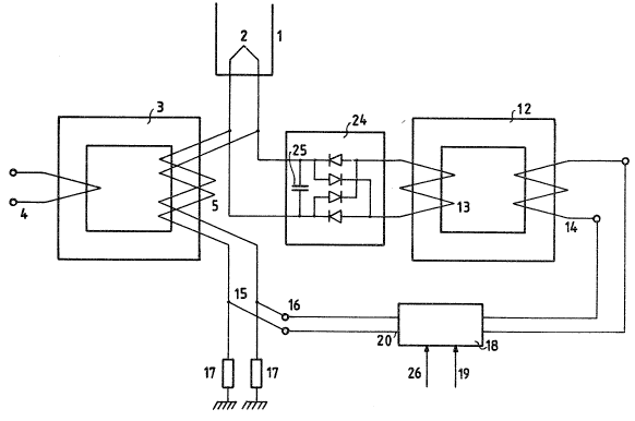
A possible embodiment of a power supply device according to the
invention is schematically presented in Fig. 3. In this embodiment,
a voltage is supplied to filament 2 from the transformer 12, to
which, as dPscribed above, an AC voltage can be supplied.
Pulse transformer 3 is provided with a bifilar secondary winding 5,
which in this case is bifilar to enable the filament voltage on the
filament 2 to be measured at the end connectors 15 of the bifilar
winding 5. To this end, these end connectors are provided with
terminals 16.
Decoupling networks 17 substantially form a short-circuit for the
high-voltage pulse, generated by the bifilar winding 5.
These end connectors 15 are therefore substantially at earth
potential. The decoupling networks 17 are, however, connected in
:
'
20~2~3~
series, parallel ~o the filament and shall therefore be designed
such that they only form a negligible load for the filament
transformer 12. A suitable decoupling network is provlded with a
capacitor, to whlch a high-ohmic resistor is connected in parallel.
During operation, the filament voltage can now be measured at the
terminals 16. This enables the filament voltage to be contlnuously
monitored.
Filament transformer 12 shall be designed such that parasitic
capacitance between primary winding 14 snd secondary winding 13 are
minimal. This parasitic capacitance is parallel to the load for the
pulse transformer 3 formed by the transmitter tube 1 and causes
a reduced slope of the pu1s2 ~ ripple during the pulse and a positive
residual voltage aPter the pulse.
In this field it is well ~nown, that low parasitic capacitance
between primary and secondary winding inevitably entails a high
leakage self-inductance in the transformer. This renders the voltage
on filament 2 dependent oi the temperature of the filament
transformer and of the frequency of the voltage on the primary
winding 14. Moreover, the voltage on the filament 2 naturally
depends on the height of ~he voltage on the pr~mary winding 14,
usually the mains voltage.
A highly advantageous embodiment of the invention offers the
possibility to connect the primary winding 14 of the filament
transformer 12 to a closed-loop regulated AC power source 18,
provided with an ad~usting device 19 for selecting the required AC
voltage. The AC power source 18 is furthermore provided with a sense
input 20, which enables the actual voltage of the filament 2 to be
measured. This measurement using the sense input 20 is performed via
the terminals 16 and the bifilar secondary winding 5 which, in turn,
is connected to the filament 2. As a result of the feedback, an
accurate and constant iilament voltage is obtained and any effects
due to the leakage self-induc~ance are eliminated.
20~2(~3~
If a re~ulated AC power source 1~ with a high frequency is selected,
for instance a switched power supply or a resonant convertor, ~he
filament transformer 12 can be designed as illustrated in Fig. 4.
Here, the core of the transformer 12 is formed by an annular core
21, whlch is wound with n primary windings 22 and with a secondary
winding, which only consists of one single winding 23. As regards
this type of transformer, it is well known in this field that
superior insulation-characteristics are coupled to a low parasitic
capacitance between the primary winding 22 and the secondary wlnding
23, the leakage self-inductance of the transformer being optimal.
The number of primary windings n can be determined by dividing the
nominal output voltage of the AC power source by the required
nominal filament voltage of the filament 2.
To effect an optimal insulation between the primary winding 22 and
the secondary winding 23, ~he ratio between the inside diameter of
annular core 21 and the outside diameter of the secondary winding 23
is selected to be approximately 2.7. As known from high-voltage
technology, the electrical field strength close to the secondary
winding will then be minimal.
In the radar transmitter tube the filament, or a cathode heated by
the filament, emits electrons under the influence of the
high-voltage pulse. It has been found, that the voltage to be
applied to the filament slightly affects the speed at which the
electrons are emitted. Consequently, the radar transmitter pulse
contains, to a limited degree, modulation sidebands with the
frequency of the filament voltage. This renders the radar
transmitter less suitable for applications where the radar is aimed
at exclusively detecting moving targets. Now that the primary
winding 14 of the filament transformer 12 ~s connected to a
high-frequency AC power source 18, it is possible to include a
rectifier circuit 24 with smoothing capacitors 25 between the
2~2~3~
secondary winding 13 of the filament transformer 12, as a result of
which the modulation sidebands will virtually disappear. High
frequency is required because the filament ls usually very
low-ohmic, which in case of low frequencies would require impossibly
large smoothing capacitors. ~hen incorporating a rectifier circuit
24, the AC power source 13 shall be provided with a sense lnput 20,
suitable for handling a ~C voltage, since the voltage to be measured
by the sense-input is of the DC type.
A further reduction of the modulation sidebands can also be
accomplished by equipping the AC power source 18 with a switching
facility 26 for switching the AC power source off, shortly before
the high-voltage pulse is applied to the radar transmitter tube and
switching it on again shortly after the high-voltage pulse. In this
case, the selected frequency of the AC power source must be
considerably higher than the repetition frequency. On the basis of
an assumed repetition frequency of 1 kHz, a pulse durat~on of the
high-voltage pulse of 1 ~sec and a frequency of the AC power source
of 100 kHz, the power source is found to be switched off
approximately 1% of the time. During this period, the smoothing
capacitors 25 of the recifier circuit 24 and the thermal capacity of
the filament 2 ensure that the filament maintains a virtually
constant temperatura.