Note: Descriptions are shown in the official language in which they were submitted.
20~2331
OPTICAI ~WITC~T~G CONNECTOR
BACKGROUND OF THE INVENTION
1. Field of the Invention
The present invention relates to an optical
switching connector used for switching optical paths of an
optical fiber line, more particularly relates to an optical
switching connector able to switch optical paths in multiple
stages of three or four stages.
2. Description of the Related Art
In the prior art, there has been known, as an
optical switching connector used for switching the optical
paths of an optical fiber line, an optical switching connector
such as shown in Figs. 24(a) and (b) (Japanese Unexamined
Published Patent Application (Kokai) No. 63-85522).
This optical switching connector has a first ferrule
11 and a second ferrule 12 disposed with end faces thereof
abutting on each other. The first ferrule 11 has two parallel
pin holes 13 and the second ferrule 12 has corresponding
parallel Pin holes 14. In the corresponding pin holes 13 and
14 are inserted reference pins 15 so as to bridge the two
ferrules 11 and 12. The pin holes 13 of the first ferrule 11
are formed in a size allowing the reference pins 15 to fit in
without clearance, while the pin holes 14 of the second
ferrule 12 are formed to have an elongated sectional shape so
~`
.. . :
.~
,
2~23~1
as to allow the reference pins 15 to move laterally by a
certain pitch P.
Between the two pin holes 13 of the first ferrule
11, for example, four optical fibers 17a to 17d incorporated
in a four-core tape-like cable 16 are affixed with the end
faces exposed. Further, between the two pin holes 14 of the
second ferrule 12, for example, two optical fibers 19a and 19b
of a two-core tape-like cable 18 are affixed with the end
faces exposed.
If the first ferrule 11 is fixed in place and the
second ferrule 12 can move laterally (reverse also possible),
in the state with force applied in the arrow A direction to
the second ferrule 12 as shown in (a) of the figure, the two
optical fibers l9a and 19b of the second ferrule 12 are
connected as optical paths with the two optical fibers 17a and
17b of the first ferrule 12. After this, if force in the
direction of the arrow B is applied to the second ferrule 12
as shown in (b) of the figure, the ferrule 12 moves laterallY
and the optical fibers 19a and 19b of the ferrule 12 are
connected as optical paths with the two optical fibers 17c and
17d of the first ferrule 11.
In this optical switching connector, the optical
paths are switched in the above way.
This type of optical switching connector is simple
in construction, so has the advantages of being relatively
.
' ' `
20~2331
easy to manufacture and being low in cost. but since the first
ferrule and -the second ferrule can onlY oppose each other in
two relative positions, switching is possible in only two
stages and therefore there was the problem of limited
application.
SUMMARY OF THE INVENTION
The present invention, in consideration of the above
problem in the related art, has as its obiect the provision of
an optical switching connector which can switch the optical
paths of optical fibers in multiple stages of three or four
stages by a simple operation and which thus enable complicated
switching of optical paths.
To achieve this object, the first optical switching
connector of the present invention is provided with a first
and second ferrule disposed with end faces thereof abutting on
each other and two reference pins disposed in parallel at a
predetermined interval, the first and second ferrules having
two parallel pin holes, respectively, the two reference pins
being inserted in the pin holes, the pin holes having an
elongated sectional shape enabling the reference pins to move
laterally by exactly a certain movement pitch. the first and
second ferrules being able to be positioned at one position
determined by one of the inside surfaces of the pin holes
being pressed against the reference pins and another position
determ;ned by the other inside surfaces of the pin holes being
2~2~31
pressed against the reference pins, one of the first and
second ferrules having two or more optical fibers affixed to
it at a pitch of 1/n (n being a posit;ve integer) of the
above-mentioned certain movement Pitch, the other ferrule
having one or more oPtical fibers affixed to it so to
correspond with all or part of the same.
The movement Pitch of the reference pins in the Pin holes
formed in the first ferrule and the movement pitch of the
reference pins in the pin holes formed in the second ferrule
preferably are the same.
In the optical switching connector, the first ferrule and
the second ferrule may face each other in the following three
positions:
(1) State where one of the inside surfaces of the Pin
holes (or the other inside surfaces) of both the first and
second ferrules are pressed against the reference pins.
(2) State where one of the inside surfaces of the Pin
holes of the first ferrule are pressed against the reference
pins and the other inside surfaces of the pin holes of the
second ferrule are pressed against -the reference pins.
(3) State where the other inside surfaces of the Pin
holes of the first ferrule are pressed against the reference
pins and the one inside surfaces of the pin holes of the
second ferrule are pressed against the reference pins.
Therefore, the first optical switching connector can
.
~- ~
. . ., . : .
- , : -
..
20~2331
switch the oPtical paths in three stages.
According to the first optical switching connector of the
presen-t invention, it is possible to obtain an optical
switching connector able to switch the oPtical paths of the
optical fibers in three stages swiftlY by a simple operation
and therefore there is the remarkable effect of enabling
switching of complicated optical paths with ease by an
inexpensive apparatus, compared with the prior art.
The second optical switching connector of the present
invention is provided with a first and second ferrule disposed
with end faces thereof abutting on against each other and two
reference pins disposed in parallel at a predetermined
interval, the first and second ferrules having two parallel
pin holes, respectively, the two reference pins being inserted
in the pin holes, the pin holes having an elongated sectional
shape enabling the ferrules to move laterally by a certain
movement Pitch with resPect to the reference pins, the first
and second ferrules being able to be positioned at one
position determined by one of the inside surfaces of the pin
holes being pressed against the reference pins and another
position determined by the other inside surfaces of the pin
holes being pressed against the reference pins, one of the
first and second ferrules having three or more optical fibers
affixed to it at a pitch of 1/n (n being a positive integer)
of the certain movement pitch, the other ferrule having one or
.~ .
: ',
~52331
more optical fibers affixed to it so as to oppose all or part
of the same.
The movement pitch of the reference pins in the Pin holes
formed in the f;rst ferrule and the movement pitch of the
reference pins in the pin holes formed in the second ferrule
preferably are different.
In the second optical switching connector, the first
ferrule and the second ferrule may face each other in the
following four positions:
(1) State where one of the inside surfaces of the pin
holes of both the first and second ferrules are pressed
against the reference pins.
(2) State where one of the inside surfaces of the pin
holes of the first ferrule are pressed against the reference
pins and the other inside surfaces of the pin holes of the
second ferrule are pressed against the reference pins.
(3) State where the other inside surfaces of the Pin
holes of the first ferrule are Pressed against the reference
pins and the one inside surfaces of the Pin holes of the
second ferrule are pressed against the reference pins.
~ ) State where the other of the inside surfaces of the
pin holes of both the first and second ferrules are pressed
against the reference pins.
Therefore, the second optical switching connector can
switch the optical paths in four stages.
- . : .
20~2331
According to the second optical switching connector of
the present invention. it is possible to obtain an optical
switching connector able to switch the optical paths of the
optical fibers in four stages swiftly bY a simple operation
and therefore there is the remarkable effect of enabling
switching of complicated optical paths with ease by an
inexpensive apparatus, compared with the prior art.
BRIEF DESCRIPTION OF THE DRAWTNGS
Figures l(a) to (d) are explanatory views showing the
switching pattern of an optical switching connector according
to one embodiment of the present invention,
Figs. 2(a) and (b) are a perspective view and frontal
view showing an example of a ferrule used in the optical
switching connector,
Figs. 3(a) to (c) are a plane view, side view, and rear
view of the overall construction of the above-mentioned
optical switching connector including the drive system,
Fig. 4 and Fig. 5 are perspective views showing other
examples of a ferrule used in the present invention,
Figs. 6(a) to (c) are sectional views showing other
examples of the shapes of Pin holes of a ferrule used in the
present invention,
Fig. 7 is a perspective view showing another example of a
support table used in the present invention,
Fig. 8 is a PerspectiVe view showing another embodiment
.
' - ' : .
, -: '. ' : .
.. ~ . .. .. .
.
-" 20~2331
of an optical switching connector according to the present
invention,
Figs. 9(a) to (c), Figs. lO(a) to (c), Figs. 11(a) to
(c), and Figs. 12(a) to (c) are explanatory views showing
other examples of the switching pattern of an optical
switching connector according to the present invention,
Figs. 13(a) to (d) are explanatory views showing a
switching pattern of an optical switching connector according
to another embodiment of the present invention,
Figs. 14(a) and (b) are a perspective view and frontal
view of a first ferrule used in the optical switching
connector,
Figs. 15(a) and (b) are a perspective view and front view
showing a second ferrule,
Figs. 16(a) to (c) are a Plane view, side view, and rear
view showing the overall construction of the above optical
switching connector including the drive system,
Fig. 17 and Fig. 18 are perspective views showing other
examples of a ferrule used in the op-tical switching connector
of the present invention,
Figs. 19(a) to (d), Figs. 20(a) to (d), Figs. 21(a) to
(d), Figs. 22(a) to (d), and Figs. 23(a) to (d) are
explanatory views showing other examples of the switching
attern of the optical switching connector according to the
; 25 present invention, and
~':
. ~ .
.::, ' ~'. .. '.: . . . '' : `
20~2331
Figs. 24(a) and (b) are explanatory views showing the
switching pattern of a conventional optical swi-tching
connector.
DESCRIPTION OF THE PREFERRED EMBODIMENTS
Below. a detailed explanation will be made of embodiments
of the present invention with reference to the drawings.
The optical switching connector of the embodiment shown
in Figs. l(a) to (d) is provided with a first ferrule 21 and
second ferrule 22 disposed with end faces thereof abutting on
each other and two reference pins 25 disposed in parallel at a
predetermined interval.
The first and second ferrules 21 and 22 each have two
parallel pin holes 23 and 24, in which the two reference pins
25 are inserted. All of the pin holes 23 and 24 are elongated
in sectional shape so as to allow the ferrules 21 and 22 to
move laterallY with respect to the reference pins 25 by a
certain pitch P. The two reference Pins 25 are fixed to a
; support table 41 as shown in Fig. 3. for example.
The first ferrule 21 has affixed to it three optical
fibers 27a to 27c. incorporated in a three-core tape-like
cable 26. at the same pitch as the movement Pitch P of the
reference pins 25 in the pin holes 23 and 24. The second
ferrule 22 has affixed to it a single optical fiber 29,
incorporated in a single core fiber cable 28. to oppose the
cable 26.
'' ' :
.. . . .
.. . . .
-`" 20~2331
The positional relationship of the optical fibers 27a to
27c and the optical fiber 29, as shown in (a) of the figure,
is such that when the first and second ferrules 21 and 22 are
pushed in the direction of the arrow A and one of the inside
surfaces 23a and 24a of the Pin holes 23 and 24 are pressed
against the reference PinS 25 in Position, the optical axes of
the optical fiber 29 and the optical fiber 27b coincide.
When, as shown in (b) of the figure, just the first
ferrule 21 is pressed in the direction of the arrow B from
this state, the first ferrule 21 moves laterally by exactly
the predetermined pitch P, the other inside surfaces 23b of
the pin holes 23 are pressed against the reference Pins 25,
and the position is thus set. In this state, the optical fiber
29 coincides in optical axis with the optical fiber 27a.
Further, as shown in (c) of the figure, when iust the
second ferrule 22 is pushed in the direction of the arrow B
from the state of (a) of the figure, the second ferrule 22
moves laterally by exactly the predetermined pitch P, the
other inside surfaces 24b of the pin holes 24 are Pressed
against the reference Pins 25, and the position is thus set.
In this state, the optical fiber 29 coincides in optical axis
with the optical fiber 27c.
When, as shown in (d) of the figure, the first ferrule 21
is Pressed in the direction of the arrow B from the state of
~` 25 (c) of the figure, the first ferrule 21 moves laterally by
:::
.. ~ ,
11 2052331 .
exactly the predetermined pitch P, the other inside surfaces
23b of the pin holes 23 are pressed against the reference pins
25, and the position is thus set. In this state, the optical
fiber 29 coincides in optical axis with the optical fiber 27b.
This is the same state of connection as in (a) of the figure,
so in the actual switching operation, either one of the states
(a) and (d) may be used.
The optical switching connector of the present invention
can switch the optical paths in three stages as explained
above.
A specific example of the ferrule used in the optical
switching connector of the Present invention will be explained
here with reference to Figs. 2(a) and (b). Here, the
explanation will be made of the first ferrule, but the second
ferrule has substantially the same construction as this.
The ferrule 21 is comprised of a base plate 31 and a
center cover plate 32 and two side cover plates 33 fixed
adhered to the top of the plate 31. The base Plate 31 has
three V-shaped grooves 34 in the top center portion and has
trapezoidal grooves 35 formed in parallel at the two sides
thereof. The V-shaped grooves 34 have three optical fibers 27a
to 27c of a tape-like cable 26 laid in them and are covered by
the center cover plate 32 affixed and adhered at the top. This
; enables the three optical fibers 27a to 27c to be affixed in a
certain position. Further, the portions of the base plate 31
`: :
12 2052331
where the trapezoidal grooves 25 are formed have the two side
cover plates 33 affixed adhered to the top. The pin holes 23
are defined by the two side cover plates 22 and the
trapezoidal grooves 35.
S The pin holes 23 have reference pins 25 inserted in them
as shown in (b) of the figure. The reference pins 25 can move
laterally relative to the ferrule 21 in the Pin holes 23. The
center distance L between the two pin holes 23 is formed so as
to accurately match the center distance ~ of the two reference
pins 25. Further, the range of possible movement of the
reference pins 25 in the pin holes 23 is designed to be within
the range of a predetermined pitch P from the Position (solid
line) where the reference pins 25 abut against one of the
inside surfaces 23a of the Pin holes 23 to the position where
they abut against the other of the inside surfaces 23b (broken
line). The three V-shaped grooves 34 are formed on the base
plate 31 at a pitch the same as this.
The base plate 31 is formed, for example, by
superfinishing grinding of ceramic or carbide alloy, by
chemical etchinK of silicon monocrystalline substrates, etc.
since a particularly hieh dimensional precision is required.
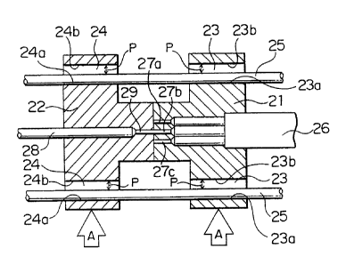
Figures 3(a) to (c) show the overall construction of an
optical switching connector including the driving system of -.
the first and second ferrules.
The two reference pins 25 inserted in the pin holes 23
- ~, : , . .
.
2~52331
13
and 24 of the first and second ferrules 21 and 22 are fixed
and supported at the two ends and the center portion to a
support table 41. Further, the rear end faces of the first and
second ferrules 21 and 22 and the two side support portions of
the support table 41 have inserted between them compression
type coil springs 42. The two ferrules 21 and Z2 are made to
press against each other at the front end faces by the
repulsion force of the springs 42.
On the oiher hand, at the bottom of the support table 41
are affixed first and second solenoids 43 and 44 corresponding
to the first and second ferrules 21 and 22. These solenoids 43
and 44 are bi-stable type solenoids where plungers 45 and 46
move back and forth in a direction perpendicular to the
reference pins 25. At the two ends of the plungers 45 and 46
are affixed rising PieceS 47 and 48. At the top end portions
of the rising pieces 47 and 48 are affixed push heads 49a,
49b, 50a, and 50b which push the side surfaces of the ferrules
21 and 22. The push heads 49a, 49b, 50a, and 50b have forward
and reverse movable push pins 51, which push pins 51 are
biased in the forward direction at all times by the
compression springs 52 in the push heads.
The reciprocal movement stroke of the plungers 45 and 46
of the solenoids 43 and 44 is set to an extent so that when
the push heads 49a and 50a push the ferrules 21 and 22, their
push pins 51 pull back to the intermediate position and
20~2331
14
conversely when the push heads 49b and SOb push the ferrules
21 and 22, their push pins 51 pull back to the intermediate
position.
In Fig. 3(a), the push heads 49a and 50a push the
ferrules 21 and 22, giving the same state as in Fig. 1(a). If
the first solenoid 43 is operated in the reverse direction
from this state, then the push head 49b will push the first
ferrule 21 from the opposite side and move the same laterally,
so the state of Fig. 1(b) will result. Further, if the second
solenoid 44 is operated in the reverse direction from the
state of Fig. 3(a), the push head 50b will push the second
ferrule from the opposite side and move the same laterally, so
the state of Fig. 1(c) will result.
The optical switching connector switches in three stages
as mentioned above.
Figure 4 shows another example of the ferrule used in the .
optical switching connector of the Present invention. The
ferrule 61 is comprised by a hard, high Precision Plastic such
as an engineering plastic and is formed, for example, by
iniection molding. Reference numeral 23 is a pin hole, 26 a
tape-like cable, and 27a to 27c are optical fibers.
Figure 5 shows a still other example of a ferrule used in
the optical switching connector of the present invention. In
this ferrule 62, a base plate 31 and two side cover plates 33
as shawn in Fig. 2 are fit into a housing 63 and affixed by
:
... .
' ~ ~
20~2331
bolts 64. At the center portion of the base plate 31 there are
formed not V-shaped grooves, but a hole with an elongated
sectional shape, in which is formed an engineering plastic or
other high precision plastic 65 by insert moiding etc. This
plastic has formed in it fine holes for insertion of the
optical fibers 27a to 27c. These fine holes are formed by
using molding pins etc. during the insert molding.
Figure 6 is a view showing another example of the pin
holes formed in the ferrule. (a) of the figure shows an
example of a Pin hole 23 formed to be an elongated triangle,
(b) shows an example of a Pin hole 23 formed to be an
elongated diamond, and (c) shows an example of a pin hole 23
formed to be an elongated rectangle. The pin holes 23 in which
the reference pins 25 are inserted are not limited to those
with such sectional shapes and may be of various other shapes
as well.
Figure 7 shows another example of the support table used
in the optical switching connector of the present invention.
In the support table 41 shown in Fig. 3, the reference pins 25
were positioned by placing them in the V-shaped grooves formed
in the support table 41. As opposed to this, in this
embodiment, the support table 66 has support holes 67 formed
in it, through which reference pins (not shown) are inserted .
to be supported. By making such a construction, it is possible
to make the support table 66 by iniection molding plastic.
~ ' ': ` ':
2~52331
16
Figure 8 shows another embodiment of the optical
switching connector of the present invention. This optical
switching connector is made of a dust-Proof construction by
covering by a box 68 and cover 69 the ferrules 21 and 22,
reference pins 25, and support table 41 of the optical
switching connec-tor shown in Fig. 3. The other parts of the
construction are the same as in the embodiment shown in Fig. 3
and the same Portions are given the same reference numerals.
Figure 9 to Fig. 12 show other examples of the switching
pattern of the optical switching connector according to the
present invention. (a) to (c) of the figures correspond to the
states of (a) to (c) in Fig. 1.
In Fig. 9, the first ferrule 21 has six optical fibers
27a to 27f affixed at pitches of 1/2 of the movement pitch P
of the ferrule 21, while the second ferrule 22 has two optical
fibers 29a and 29b affixed at the same pitch. By doing this,
as shown in (a) to (c) of the figure, it is possible to
perform switching of the optical paths of 2 vs. 6 optical
fibers in three stages.
By the same method as this, for example, the first
ferrule may have nine optical fibers affixed to it at a pitch
of lt3 of the ferrule movement pitch P and the second ferrule
may have three optical fibers affixed at the same pitch,
whereby it is possible ~o perform switching of the optical
paths of 3 vs. 9 optical fibers in three stages.
17 2052331
In the embodiment shown in Fig. 10, the first and second
ferrules 21 and 22 have six optical fibers 27a to 27f and 29a
to 29f affixed to them at a pitch the same as the ferrule
movement pitch P so that as shown in (a) to (c) of the figure,
6 vs. 6 switching is performed in three stages.
In the embodiment shown in Fig. 11, the first and second
ferrules 21 and 22 have two optical fibers 27a, 27b and 29a,
29b affixed to them at a pitch the same as the ferrule
movement pitch P so that as shown in (a) to tc) of the figure,
2 vs. 2 switching is performed in -three stages.
In the embodiment shown in Fig. 12, the ferrule 21 has
two optical fibers 27a and 27b affixed to them at a pitch the
same as the movement pitch P of the ferrule 21 and the second
ferrule 22 has a single optical fiber 29 affixed to it, so
that 1 vs. 2 switchinK, including non-connection, is performed
in three stages.
Next, an explanation will be made of an embodiment of an
optical switching connector enabling switching in faur stages.
The oPtical switching connector according to the
embodiment shown in Figs. 13(a) to (d) is Provided with a
first ferrule 121 and second ferrule 122 disposed with their
end faces abutting on each other and two reference Pins 125
disposed in parallel at a predetermined interval.
The first and second ferrules 121 and 122 each have two
parallel Pin holes 123 and 124, which Pin holes 123 and 124
'
.
.
:
2~233~
18
have the above two reference pins 125 inserted through them.
The two reference pins 125 are affixed to the support table
141 shown in Fig. 16. for example.
The pin holes 123 of the first ferrule 121 are elongated
in sectional shaPe so as to allow lateral movement of the
ferrule 121 by exactly a certain pitch P with respect to the
reference pins 125. Further, the pin holes 124 of the second
ferrule 122 are elongated in sec-tional shape so as to allow
lateral movement of the ferrule 122 bY exactlY a certain pitch
P with respect to the reference pins 125.
The first ferrule 121 has four optical fibers 127a to
127d affixed by a pitch the same as the movement pitch P of
the reference pins 125 in the pin holes 123, while the second
ferrule 122 has one optical fiber 129 affixed to it to oppose
the same.
The Positional relationship of the optical fibers 127a to
127d and the optical fiber 129, as shown in (a) of the figure,
is such that when the first and second ferrules 121 and 122
are pushed in the direction of the arrow A and one of the
inside surfaces 123a and 124a of the pin holes 123 and 124 are
pressed against the reference pins 125 in position, the
optical axes of the optical fiber 129 and the optical fiber
127b coincide.
When, as shown in (b) of the figure, just the first
ferrule 121 is pressed in the direction of the arrow B from
... . . ~ : .
.
.
20~2331
19
this state, the first ferrule 121 moves laterally by exactly
the predetermined pitch P, the other inside surfaces 123b of
the pin holes 123 are pressed against the pin holes 125, and
the position is thus set. In this state, the optical fiber 129
coincides in optical axis with the optical fiber 127d.
Further, as shown in (c) of the figure, when iust the
second ferrule 122 is pushed in the direction of the arrow B
from the state of ~a) of the figure, the second ferrule 122
moves laterally by exactly the predetermined pitch P, the
other inside surfaces 124b of the pin holes 124 are pressed
against the reference pins 125, and the position is thus set.
In this state, the optical fiber 129 coincides in optical axis
with the oPtical fiber 127a.
When, as shown in (d) of the figure, the first ferrule
121 is Pressed in the direction of the arrow B from the state
of (c) of the figure, the first ferrule 121 moves laterally by
exactly the predetermined pitch P, the other inside surfaces
123b of the pin holes 123 are pressed against the pin holes
125, and the position is thus set. In this state, the optical
fiber 129 coincides in optical axis with the optical fiber
127b.
The optical switching connector of the PreSent invention
can switch the optical paths in four stages as explained
above.
Next, a specific example of the ferrule used in the
- , ,
:
20~233~
optical switching connector able to switch in four stages will
be explained with reference -to Fig. 14 and Fig. 15.
Figure 14(a) and (b) show the first ferrule 121. The
ferrule 121 is comprised of a base plate 131 and a center
cover plate 132 and two side cover plates 133 fixed adhered -to
the top of the plate 131. The base plate 131 has four V-shaped
grooves 134 in the top center portion at a Predetermined pitch
P and has trapezoidal grooves 135 formed in parallel at the
two sides thereof. The V-shaped grooves 134 have four optical
fibers 127a to 127d of a tape-like cable 126 laid in them and
are covered by the center cover Plate 132 affixed and adhered
at the top. This enables the four optical fibers 127a to 127d
to be affixed in a certain position. Further, the Portions of
the base plate 131 where the trapezoidal grooves 135 are
]5 formed have the two side cover plates 133 affixed adhered to
the top. The pin holes 123 are defined by the two side cover
plates 133 and the trapezoidal grooves 135.
The pin holes 123 have reference pins 125 inserted in
them as shown in (b) of the figure. The reference pins 125 can
move laterally relative to the ferrule 121 in the pln holes
123. The center distance L between the two pin holes 123 is
formed so as to accurately match the center distance ~ of the
two reference pins 125. Further, the range of possible
movement of the reference pins 125 in the pin holes 123 is
designed to be within the range of a predetermined pitch P
. .
~ ~ ~ ."'' '-
~ ~ ' ' ' ' ,
- 20S233~
21
from the position (solid line) where the reference pins 125
abut against one of the inside surfaces 123a of the pin holes
123 to the position where they abut against the other of the
inside surfaces 123b (broken line). The four V-shaped grooves
134 are formed on the base plate 131 at a pitch P the same as
this.
Figures 15(a) and (b) show a second ferrule 122. The
ferrule 122 is comprised of a base plate 136 and a center
cover plate 137 and two side cover plates 138 fixed adhered to
the top of the same. The base plate 136 has a single V-shaped
groove 139 in the top center portion and has traPezoidal
grooves 140 formed in parallel at the two sides thereof. The
V-shaped groove 139 has an optical fiber 129 of a single-core
optical fiber cable 128 laid in it and are covered by the
center cover plate 137 affixed and adhered at the top. This
enables the optical fiber 129 to be affixed in a certain
position. Further, the portions of the base plate 136 where
the trapezoidal grooves 140 are formed have the two side cover
plates 138 affixed adhered to the top. The Pin holes 124 are
defined by the two side cover plates 138 and the trapezoidal
grooves 140.
The pin holes 124 have reference pins 125 inserted in
them as shown in (b) of the figure. The reference Pins 125 can
; move laterallY relative to the ferrule 122 in the pin holes
124. The relationship between the two Pin holes 124 and the
. .
- . :
` 20~2331
22
reference PinS 125 is the same as the relationshiP between the
pin holes 123 and the reference pins 125 shown in Fig. 14(b)
except that the reference pins 125 can move in the pin holes
124 laterally at a pitch 2P twice the movement pitch P of the
reference pins 125 in the pin holes 123 of the first ferrule
121 shown in Fig. 14(b).
Note that the base plates 131 and 136 are formed, for
example, by ultraprecision grinding of ceramic or ultrahard
alloy, by chemical etching of silicon monocrYstalline
substrates, etc. since a particularly high dimensional
precision is required.
Figures ]6(a) to (c) show the overall construction of an
optical switching connector including the driving system of
the first and second ferrules.
The two reference pins 125 inserted in the Pin holes 123
and 124 of the first and second ferrules 121 and 122 are fixed
and supported at the two ends and the center portion to a
support table 141. Further, the rear end faces of the first
and second ferrules 121 and 122 and the two side support
Portions of the support table 141 have inserted between them
compression type coil springs 142. The two ferrules 121 and
122 are made to press against each other at the front end
faces by the repulsion force of the sPring 142.
On the other hand, at the bottom of the support table 141
are affixed first and second solenoids 143 and 144
,
2052331
corresponding to the first and second ferrules 121 and 122.
These solenoids 143 and 144 are bistable type solenoids where
plungers 145 and 146 move back and forth in a direction
perpendicular to the reference pins 125. At the two ends of
the plungers 145 and 146 are affixed rising pieces 147 and
148. At the top end portions of the rising pieces 147 and 148
are affixed Push heads 149a, 149b, 150a, and 150b which push
the side surfaces of the ferrules 121 and 122. The push heads
149a, 149b, 150a, and 150b have forward and reverse movable
push pins 151, which push pins 151 are biased in the forward
(protruding) direction at all times by the compression springs
152 in the push heads.
The reciprocal movement stroke of the plungers 145 and
146 of the solenoids 143 and 144 is set to an extent so that
when the Push heads 149a and 150a push the ferrules 121 and
122, their push pins 151 pull back to the intermediate
position and conversely when the Push heads 149b and 150b push
the ferrules 121 and 122, their push Pins 151 pull back to the
intermediate position.
In Fig. 16(a), the push heads 149a and 150a push the
ferrules 121 and 122, giving the same state as in Fig. 13(d).
If the first solenoid 143 is operated in the reverse direction
from this state, then the Push head 149a will push the first
ferrule 121 from the opposite side and move the same
laterally, so the state of Fig. 13(c) will result. Further, if
2052331
24
the second solenoid 144 is operated in the reverse direction
frorn the state of Fig. 16(a), the push head 150a will push the
second ferrule 122 from the opposite side and move the same
laterally, so the state of Fig. 13(b) will result. lf the
first solenoid 143 is operated in the reverse direction from
this state, then the push head 149a will push the first
ferrule 121 from the opposite side and move the same
laterally, so the state of Fig. 13(a) will result.
The optical switching connector can switch in four stages
as mentioned above.
Figure 17 shows another examPle of the ferrule able to
switch in four stages. The first and second ferrules 121 and
122 are comprised by a hard, high precision plastic such as an
engineering plastic and is formed, for example, by molding.
Reference numerals 123 and 124 are pin holes, 126 a tape-like
cable, 127a to 127c optical fibers, 128 a single core optical
fiber cable, and 129 an optical fiber.
Figure 18 shows a still other example of a ferrule used
in the optical switching connector able to switch in four
; 20 stages. In this ferrule 121, a base plate 131 and two side
cover plates 133 as shown in Fig. 14 are fit into a housing
~ 161 and affixed by bolts 162. At the center Portion of the
; base plate ~31 there are formed not V-shaped grooves, but a
hole with an elongated sectional shape, in which is filled an
engineering plastic or other high precision plastic 163. This
25 20~2331
plastic 163 is formed, for example, by insert molding and has
formed in it fine holes for insertion of the optical fibers
127a to 127d. In the second ferrule 122 too, a base plate 136
and two side cover plates 138 as shown in Fig. 15 are fit into
a housing 164 and affixed by bolts 165. At the center portion
of the base plate 165 there are formed not V-shaped grooves,
but a hole with an elongated sectional shape, in which is
filled an engineering plastic or other high precision plastic
163. This plastic 163 is formed, for example, by insert
molding and has formed in it a fine hole for insertion of the
optical fiber 129.
The shape of the pin holes formed in the ferrules is not
particularly limited, but the various shapes shown in Fig. 6
may be used. Further, the support table used in the optical
switching connector able to switch in four stages is not
particularly limited. and the support table 41 shown in Fig. 7
may be used. With such a construction, it is possible to
produce the support table 41 by iniection molding and to keep
costs low. Further, like with the optical switching connector
able to switch in three stages, the connector may be made a
dust-proof construction as shown in Fig. 8.
Figure 19 to Fig. 23 show other examples of a switching
pattern of an optical switching connector able to switch in
four stages according to the present invention. (a) to td) of
the figures correspond to the states (a) to (d) of Fig. 13.
.
~ ,.: ~-. . .
---" 20~2331
26
In the embodiment shown in Fig. 19, the first ferrule 121
has eigh-t optical fibers 127a to 127h affixed at a pitch of
1/2 of the movement pitch P of the ferrule 121, while the
second ferrule 122 has two optical fibers 129a and 129b fixed
at the same pitch. By doing this, as shown in (a) to (d) of
the figure, it is Possible to switch the optical paths of 2
vs. 8 optical fibers in four stages.
If, bY the same method, the first ferrule has 12 optical
fibers affixed to it at a pitch of 1/3 of the movement pitch P
of the ferrule and the second ferrule has three optical fibers
affixed at the same pitch, it is possible to perform switching
of optical paths of 3 vs. 12 optical fibers in four stages.
In the embodiment shown in Fig. 20, the first and second
ferrules 121 and 122 each have six optical fibers 127a to 127f
and 129a to 129f affixed at the same pitch as the movement
pitch P of the first ferrule 121 to perform 6 vs. 6 switching
in four stages as shown in (a) to (d) of the figure.
In the embodiment shown in Fig. 21, the first ferrule 121
has three optical fibers 127a to 127c and the second ferrule
122 has two optical fibers 129a and 129b affixed at the same
itch as the movement Pitch P of the first ferrule 121, to
enable 2 vs. 3 switching in four stages as shown in (a) to (d)
of the figure. In this switching method, it becomes possible
for any optical fiber to connect with all opposing optical
fibers.
.
~ ~ `
20~2331
In the embodiment shown in Fig. 22, the first ferrule 121
has three optical fibers 127a to 127c affixed at the same
pitch as the movement pitch P of the ferrule 121, while the
second ferrule 122 has one optical fiber 129 affixed to enable
1 vs. 3 switching, including nonconnection, in four stages.
In the embodiment shown in Fig. 23, the first ferrule 121
has one optical fiber 127 affixed to it and the second ferrule
122 has four optical fibers 129a to 129d affixed to it at the
same Pitch as the movement pitch P of the first ferrule 121.
That is, the numbers of the optical fibers affixed to the
first and second ferrules 121 and 122 are reverse to the case
of Fig. 13. In this waY, even if the numbers of optical fibers
affixed to the first and second ferrules are reverse in the
above embodiments, the same four stage switching is possible.
Note that in the embodiments shown in Figs. 13 to 23, the
movement Pitch P of the reference pins 125 in the pin holes
124 formed in the second ferrule 122 was made to be twice the
movement pitch P of the reference pins 125 in the pin holes
123 formed in the first ferrule 121, but in this invention, it
may be made so that other multiPles are attained.
. .