Note: Descriptions are shown in the official language in which they were submitted.
-1- 20~23:~3
NI-CAD B~TTERY CHARC~E R~'['E CONTROLLER
The present invention relates to a method of
controlling the charge rate of a nickel-cadmium (Ni-
Cad) battery charger installed in a computer system.
Some computer systems use a Ni-Cad battery to
provide the power to the computer when an alte~nating
current (ac) outlet is inconvenient or unavailable.
The Ni-Cad battery is eventually drained and an ac
power source is necessary to run the computer and/or
recharge the Ni-Cad battery. The computer uses a Ni-
Cad battery charger which controls the energy supplied
during charging of the Ni-Cad battery.
Many techniques are available to charge Ni-Cad
batteries. The quickest method i5 to charge the
battery at a very high rate until it is fully charged
and then to switch into a very slow rate, ox trickle
rate, to maintain that charge. The rate of charge
depends upon the amount of current forced through the
battery. A fast charge uses a high amount of current
and a slow charge uses a relatively low amount of
current. A Ni-Cad battery used in computers
conventionally contains one or more individual Ni-Cad
cells. The amount of current used to determine the
charge rate depends upon the number of cells in the
battery, the state of the cells in the battery, the
power rating of each cell and other characteristLcs of
the particular cells~
-2- 2~23~3
Ni-Cad batteries requirP special handling and
control during fast charging to prevent overheating and
damage. The battery charge controller must contain
adequate monitoring devices and circuitry to charge the
Ni-Cad battery at diferent rates, to detect the status
of parametPrs such as voltage and temperature of the
battery, especially at higher rates of charge, and to
switch from one charge rate to another. Additionally,
if the Ni-Cad battery is deeply discharged, if a fast
charge is supplled, the battery may draw too much
energy and interfere with computer operation by drawing
down the voltage. The battery charge control circuitry
must also compensate for this condition. 8attery
chargers may, therefore, require complex circuitry as
well as expensive components to achieve these tasks.
The present invention provides control over the
charge rate of a Ni-Cad battery by switching a current
limiter in or out of the charging circuit depending
upon the status of the Ni-Cad. A simple current
limiter utilizing a common discrete component limits
the current of a Ni-Cad charger to the required trickle
rate for slow charge. FET power transistors are
configured as a switch such that when they are turned
on they simultaneously by-pass and disable the current
limiter and allow the Ni-Cad battery to charge at a
fast rate. A current sense resistor is connected
between the current limiter and ground to allow
m~nitoring of the charge current. The drain and source
voltages o~ the FET power transistors corresponding to
the oharge current, as well as the tempera~ure and
voltage of the Ni-Cad ~attery, are monitor~d to
determine the battery status. The gate voltage of the
FET transistors is controlled to switch the current
limiter in or out depending upon the battery status.
~ ~ ~ 2 ~ !~ .3
~3--
~he limiter is switched in when the conditions indicate
trickle or slow charge is proper and switched out when
a fast charge or discharge is appropriate.
A better understanding of the present invention
can be obtained when the following detailed description
of the preferred embodiment is considered in
conjunction with the following drawings, in which:
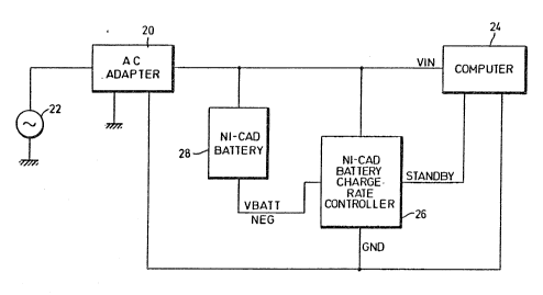
Figure 1 is a bloc~ diagram of a computer system
utilizing Ni-Cad batteries and a battery charge rate
controller according to the present invention;
Figure 2 is a schematic diagram o~ a circuit
implementation of the Ni-Cad battery charge rate
controller of Figure l; and
Figure 3 is a schematic diagram showing the logic
of the status and control block of Figure 2.
Figure 1 shows a block diagram of a computer
system using a Ni-Cad battery 28 and a Ni-Cad battery
charge rate controller 26. An ac adaptor 20 is
connected to an ac power source 22. The ac adaptor 20
converts the ac voltage to dc voltage which is used to
power the computer 24. The positive supply output is
referred to as VIN, while the negative supply is
considered ground. The ac adaptor 20 is either output
current or output power limited to prevent possible
overcl~rrent in the Ni-Cad battery 28 during fast charge
mode. The current or power limits are set as
appropriate for the particul~r cells forming the Ni-Cad
battery 2~. The ac adapter 20 also supplies power to
the Ni-Cad battery charge rate controller 26, which is
connected between the positive supply VIN and ground.
The Ni-Cad battery 28 has its positive ter~in~l
conne~ted to the positlve ~upply VIN and it~ nega~ive
.. .
- , ; .-: . .
. . : -
. ~
., . ~ . . ... . . ~ -
~ ~4~ 3 ~ 3
terminal connected to the Ni-Cad battery charge rate
controller 26 as shown by the VBATTNEG signal.
The Ni-Cad battery charge rate controller 26
controls the rate of charging of the Ni-Cad battery 28,
S either fast charge or trickle charge, when the ac
adaptor 20 is active and allows the Ni-Cad battery 28
to power the computer 24 when the ac adaptor 20 is not
active. Additionally, the Ni-Cad battery charge rate
controller 26 receives a signal referred to as STANDBY
from the computer 24. The computer 24 provides this
signal wh~n the computer 24 is entering or is in very
low power state and is used to conserve energy and
extend battery life. The STANDBY signal is used by the
Ni-Cad battery charge rate controller 26 to reduce the
controller's own power consumpti~n, thus allowing even
greater energy savings. Preferably the Ni-Cad battery
charge rate controller 26 and the Ni-Cad battery 28 are
combined in a single physical unit ~or reasons to be
explained later.
Figure 2 is a more detailed schematic showing the
Ni-Cad battery 28 connected to the Ni-Cad battery
charge rate controller 26. A transorb 42, connected
between VIN and ground, is an electrostatic detection
device which protects the Ni-Cad battery charge rate
controller 26 circuit~y from voltage transients and
electro~tatic discharges. A PNP pass transistor 52 has
its emitter connected to the VIN signal and is used to
disable the circuitry of the Ni-Cad battery charge rate
controller 26 during low power consumption or standby
periods. A resistor 48 is provided ~rom the emitter to
the base of the transistor 52, with a second resistor
50 connected between the base and the STANDBY signal
input. A capacitor 46 is connected between the VIN
signal ahd the STANDBY signal for electrosta~ic ~
discharge purposes. A capacitor 44 is connected
.- , , , , " . " , :., . : , ,
2 ~
~5-
between the STANDBY signal input and ground. When the
STANDBY signal is held at a low level by the computer
24, indicating full power operational status, the
trancistor 52 is active and passes the VIN signal to
the controller, thus passing the supply voltage t-o the
remaining circuitry. If the STANDBY signal is raised
to a high level, or preferably simply not driven, as
would occur when the Ni-Cad battery 28 and controller
26 are removed from computer 24, the capacitor 44
charges and the transistor 52 eventually shuts off.
This stops current flow through the transistor 52,
disabling the remaining circuitry. This disabled
condition thus reduces battery drain, either when the
computer 24 is in STANDBY or the battery 28 is removed.
If the ST~NDBY signal is low, dc power from the ac
adaptor 20 provides power to the input o~ a micropower
voltage regulator 54, such as an LP~951 from National
Semiconductor, through a resistor 56. The resistor 56
limits input current. A capacitor 58 is connected
between the input and ground to reduce noise at the
voltage regulator 54 input. A Zener diode 60 has its
cathode connected to the input and its anode connected
to ground to protect the voltage re~ulator 54. The
voltage regulator 54 supplies 10 volts (+lOV) for use
by the charge rate controller 26 circuitry. A resistor
voltage divider formed by resistors 62 and 64 connected
between ~lOV and ground establishes a feedback path to
the voltage regula~or 54 to determine and maintain the
output voltage at +lOV. A capacitor 66 is connected
from the ~lOV line to the junction of the resistors 62
and 64 for ~eedback loop compensation. ~ capacitor ~8
is connected between llOY and ground to act as the main
+lOY power supply ~ilter capacitor. A diode 70 has its
anode connected to the output of the voltage reg~lator
54 and its cathode connected to the coll~ctor of the
-6-
pass tra~sistor 52 for reverse voltage protection. The
voltage regulator 54 further includes an inverted error
output which, when low, indicates either a power-up
condition or a low output voltage. The error output is
pulled up to the +lOV level by a resistor 1~0 an~ is
coupled to ground by a noise filtering capacitor 142.
A current limiter 72 controls the ~rickle current
during 610w or trickle charge periods. Preferably, the
current limiter 72 includes a conventional low power
adjustable voltage regulator 73 such as an LM317 from
National Semiconductor. The voltage input terminal of
the current limiter 72, and the regulator 73, is
connected to the VBATTNEG input of the controller 26.
The maximum amount of current, or the current limit, is
detexmined by a resistor 74 connected between the
adjustment and voltage output terminals of the
regulator 73. The resistor 74 value is chosen to limit
the current to the proper amount of trickle current for
the Ni-Cad battery 28 according to the manufacturer's
recommendations and conventional limits. A charge
current sense resistor 76 is connected between the
adjustment terminal of the regulator 73 and ground. A
diode 146 has its cathode connected to the VBATTNEG
terminal and its anode connected to ground to allow
current ~low when the batteries are discharging in
order to bypass the sense resistor 76 during short
circuit discharge conditions. Discharge occurs in the
preferred embodiment only when the ac adaptor 20 is off
and the computer system is battery powered.
A pair of parallel n channel enhanceme~t FET power
transistors 78 and 80 have their drains and sources
connected from the V~3ATTNEG input to the adjustment
terminal o~ regulator 73, thus paralleling the current
limiter 72. The voltage at the drain is referr~d ~o as
Vd and the voltage at the source is referred to as V~.
.. . , . . ............. .. .. , - ..... . .... .. .. .. ... .
,. ; . .. , , , ~ . ,.: . ~ : .. .. . . ~.
--7
Filtering capacitors 102 and 112 are connected,
respectively, from the drains and the sources of the
transistors 78 and 80 to ground. A signal referr~d to
as Vg is provided to the gates of the transistors 78
and 80. In this configura~ion, when the V~ 6ignal
level is low, the transistors 78 and 80 are turned off
50 that the effective resistance between the FET drain
voltage Vd and source voltage VB is extremely high.
The FET transistors consequently appear as open
circuits to the current limiter 72. Therefore, all the
current charging the Ni-Cad battery 28 must pass
through the current limiter 72. Because the current
limiter 72 is ~et to limit at the trickle charge rate,
this Vg signal off condition thus defines the trickle
or slow charge ~ode. When a proper high level Vg
signal is applied, both FET transistors 78 and 80 turn
on, which effectively bypasses or shorts out the
current limiter 72. This bypassing allows the ac
adaptor 20 to charge the Ni-Cad batt~ry 28 at a fast
rate, up to the current or power limits of the ac
adaptor 20, or allow a low voltage drop during battery
discharge conditions. As noted, the current or power
limit of the ac adaptor 20 is set such that even at
full delivery the charge rate o~ the Ni-Cad battery 28
is within acceptable limits. Thus, proper control of
the Vg signal level sets trickle or fast charge mode.
A temperature sensor 82 monit~rs the temperature
of the Ni-Cad battery 28. The temperature sensor 82 is
preferably in good thermal contact with the Ni-Cad
battery 28 to allow the thermal sensor 82 to accurately
determine the temperature of the cell~ to prevent
damage. For this reason the controller 26 is
preferably confined in the same physical unit as the
Ni-Cad battery 28. The temperature sensor 82 re~eives
power from the ~lOV developed by the regulator 54 and
,, , . , , ,;
-8- 2 ~ 3 .~ 3
provides an output signal referred to as Vo. The value
of the signal Vo is proportional to the temperature to
allow comparison for protection and control purposes.
The Vo si~nal is connPcted to ground by a resistor B4.
A resistor 86 is connected between the Vo signal and a
signal referred to as T. The T signal is connected to
ground by capacitor 88. Thus the T signal is a
~lltered version of the Vo signal.
A control module 90 monitors the Ni-Cad battery 28
voltage, charge rate, and temperature and outputs the
Vg signal to control the FET transistors 78 and 80.
The control module 90 receives the Vd and V8 levels
through series protection resistors 100 and 110,
respectively. Similarly, the co~trol module go
provides the Vg signal through a series resistor 92. A
RESET~- input of the control module 90 is connected to
the inverted error output of the voltage regulator 54,
which is low during startup conditions or other low
output voltage conditions. Capacitors 134 and 136 are
connected between the TCAP2 and TCAPl inputs of the
control module 90 and ground, while a resistor 132 is
connected between the TRES input and ground, with a
capacitor 138 connected between the TRE5 input and
~lOV. The capacitors 134 and 136 and resistor 132 are
used as the timing components for an oscillator in the
control module 90. A power supply decoupling capacitor
144 is connected between ~lOV and ground for removing
noise at the control module 90. The control module 90
also receives the T signal to allow temperature
monitorinq.
A series of four reference voltages are developed
for use by the control module 90 in various
comparisons. The inputs are re~erred to as VREF4,
V~EF3, VREF2, and VREF1. Each of these inputs ia~
connected to ground by a capacitor 130, 124, 128 sr
,' ,:~ ,. . ,, ' ~
2~23~3
g
126, respectively, for noise rontrol purposes. The
actual voltage levels are developed by the series
combinations of resistors 122, 120, 118, 116 and 114,
which are connected between ~lOV and ground.` The
junction between the resistors 122 and 120 is connected
to the VREF4 input, while the junction between the
resistors 120 and 118 is connected to the VREF2 input.
The junction of the resistors 118 and 116 is connected
to the VREF1 input, while the remaining junction
between the resistors 116 and 114 is connected to the
VREF3 input.
The final inputs to the control module 90, besides
power and ground, are the VBATT/ 5 and the VD/5 inputs.
These signals are used to determine the actual voltage
of the Ni-Cad battery 28 to prevent an overcurrent
condition when the voltage is too low or reversed and
only trickle charging is proper. The VBATT/S input is
connected to the junction of two series resistors 94
and 96 which are connected between the collector of
transistor 52 and ground. A capacitor 98 parallels the
resistor 96 for noise filtering. The VD/5 input is
connected to the junction of two series resistors 104
and 106 which are connected between Vd and ground. A
noise capacitor 108 parallels the resistor 106.
The logic o~ the.control module 90 is shown in
Figure 3. A comparator 160 compares the temperature
sense voltage T with the reference voltage VREF1. The
level of voltage VRE~1 preferably corresponds to a
temperature of 10 celsius (C) so that the output
signal A is asserted low when the battery temperature
rises above 10C and is ~sserted high when the
temperature fall~ below 10C.
A comparator 162 compares the temperature sense
voltage T with the reference voltage YREF2. TheJlevel
of voltage VREF2 preferably corresponds to a
-lO- 20~3~.3
temperature of 400c, so that the output signal B is
asserted high when the battery temperature is below 400
C and asserted low if the battery temperature rises
above 40 C. A NOR gate 164 negates the signal B. The
A signal and the output of the NOR gate 164 are the
inputs to a two input NOR gate 166~ The NOR g~te 166
thus asserts its output high when the battery
temperature i~ between 10C and 40C, which corresponds
to the allowable temperature range for fast charging
the Ni-Cad battery 28 in the preferred embodiment.
A comparator 168 compares the voltage VS, input
from the VB signal, with the reference voltage VREF3
and asserts its output low when the level of the
voltage VS is greater than the reference voltage VREF3.
As previously noted, the voltage Vg is proportional to
the charge current flowing through the sense resistor
76. Thus the voltage VS will be a low level during
trickle charge, will be negative during discharge and
will be a higher level during fast charge. If the
output vf the comparator 168 is as~erted low, this
implies that the battery is being charged at the fast
rate. A delay d~vice 178 is connected to the output of
the comparator 168 and outputs a signal referred to as
C. The C signal is thus a delayed version of the
output of the compara~or 168. The delay device 178
receives a signal referred to as OSC from an oscillator
176. The OSC signal is used to produce the delay. The
C signal is provided as one input to a two input XOR
gate 170 and to the D input of a D-type flip-flop 174.
The second input to the XOR gate 170 is provided by the
Q output of the flip-flop 174, a signal referred to as
DC. The flip-flop 174 is used to provide a delay ~or
the sense voltage comparison to prevent power supply
transients, such as those developed by turning o~ the
computer system or specific components, fro~ falsely
: ~ : ; , ,.;. , .; , . , :
. . . ~ . , . , ,,: : ~ . , . - . .:
~ 2.~ 3
indicating a low current state. The output of the XOR
gate 170 is provided to one input of a two input NAND
gate 172. The Recond input of the NAND gate 172 is
provided by the RES~T- signal, which is the inverted
error signal from the voltage regulator 54~ The~output
of the NAN3 gate 172 is provided to the clear input of
the oscillator 176. The clock input of the flip-flop
174 is connected to the CLK signal output of the
oscillator 176.
The time of delay between the flip-flop 174 input
signal C and the output signal DC is determined by the
oscillator 176, the external capacitor 136 connected to
the TCAP1 input and the external resistor 132 connected
to the TRES input of the oscillator 176. If signal C
is equal to signal DC, the XOR gate 170 will assert its
output low which will cause the NAND gate 172 to assert
its output high, and thus the clear input to the
oscillator 176 will be high. This causes the
oscillator 176 to short the input capacitor 136 to
ground. The oscillator 176 output signal CLX,
determined by the voltage across capacitor 136 is,
therefore, set low. If signal C then changes so that
it is not equal to signal DC, the XOR gate 170 asserts
its output high, and assuming the RESET- signal is high
also, the NAND gate 172 asserts its signal low which
also sets the clear input of the oscillator 176 low.
The oscillator 176 then charges capacitor 136 through
resistor 132. The time the voltage across capacitor
136 takes to rise from low to high depends on the
values of resistor 132 and capacitor 136, and the time
should preferably range from one to six seconds. The
CLK output signal of oscillator 176 will thus rise,
causing the clock input of the flip-flop 174. to rise
accordingly. When the clock input of the flip-fLop 174
reaches a high level, the flip-flop 174 will $ransfer
- : . .
~9~23~3
-12-
its C input to the DC output, causing the signals to be
equal. The XOR gate 170 will then assert its output
low, causing the NAND gate 172 to assert its output
high, whieh causes the oscillator 176 to short
capacitor 136 to ground. The output signal CLK will,
therefore, go low, causing the flip-flop 174 alock
input to go low also. Therefore, the signal C is
transferred to 6ignal DC after a delay of one to six
~econds.
The oscillator 176 generates a free running timing
clock referred to as the OSC signal, which i5 output to
the delay device 178. An external capacitor 134 is
connected between the TCAP2 input of the oscillator 176
and ground. The frequency of the OSC signal is
determined by the resistor 132 and the capacitor 134.
The resistor 132 and the capacitor 134 should
preferably be chosen so that the frequency of signal
05C is between 200 hertz and 2 kilohertz.
A two input NOR gate 180 receives ~s inputs the
high temperature si~nal B and the delayed fast charge
signal DC output by the flip-flop 174. Thus the output
of the NOR gate 180 i5 high when the battery
temperature is above 40O r and the battery 28 is being
charged in the fast mode. This is an indication that
the battery 28 is fully charged and the charge mode
should ohange from fast to trickle. A pair of two
input NOR gates 182 and 184 are configured as an S-R
latch. The output o~ the NOR gate 180 is provided as
one input to the NOR gate 182, while the other input is
connected to the output of the NOR gate 184. The
output of the NOR gate 184 is referred to as the E
signalO The output of the NOR gate 182 is connected to
one input of the NOR gate 184. The second inpu~ is
provided by the output of a two input OR gate 196. If
the output of NOR gate 180 goes high, indicating time
-13- 2 ~
to enter trickle charge mode, the S-R latch formed by
the NOR gates 182 and 184 is set and the E signal goes
high, the output of the OR gate 196 ~eing low during
charging operations.
A ~omparator 186 compares the FET drain voltage
V~, input as VD, with the reference voltage VREFl. The
output signal referred to as D is asserted low when the
voltage VD is greater than the reference voltage VREFl,
which implies that the Ni-Cad battery 28 is being
charged in slow mode. If the FET transistors 78 and 80
are turned on, or the battery 28 is discharging, the
level of the voltage VD falls below the level of the
reference voltage VREFl and the D signal is set high.
A diode 188 and a Zener diode 190 are connected between
the VD input and ground to protect the control module
90 by clamping the VD input to a suitable level if a
deeply discharged Ni-Cad battery 28 is piaced between
VIN and VBATTNEG.
The C and D signals are the two inputs to a two
input AND gate 192. The output of the AND gate 192 is
high, therefore, i~ the battery 28 is not being charged
at all or is being discharged. The output of the AND
gate 192 is provided as one input to the OR gate 196.
The ~econd input to the OR gate 196 is provided by the
output o~ an inverter 194. The RESET- signal is
connected to the input of the inverter 194. Thus the
output of the OR gata 196 goes ~igh if a reset is
indicated or if the battery 28 is not being charged in
the fast or tr~ckle modes. Because the ac adap~or 20
preferably always provides sufficient power to charge
~hP battery 28 when active, this not fast and not
trickle mode indicates battery powered operation, so
that discharge is occurring and it may be appropriate
to try fast charging the battery 28 when the ac adaptor
20 is next active and is appropriate to turn on the
.
"~ , . . . , ~ .
~ ;. ~ . ,
;, ~
~ ~23 ~s~
-14-
transistors 78 and 80 to allow a low voltage drop
during discharge. Thus the high level from the OR gate
196 clears the S-R latch formed by the NOR gates 182
and 184.
A two input NOR gate 198 receives as inputs~the
outputs of the NOR gate 166 and the OR gate 196. The
output of the NOR gate 1~8 indicates, when low, that
the battery temperature is acceptable for fast charging
or the battery 28 is not charging.
A difference amplifier 200 su~tracts the divided
drain voltage VD/5 from the divided battery voltage
VBATT/5. The difference ~etween the VBATT/5 and VD/5
voltages represents the battery voltage divided by
five. This difference voltage is then compared to the
reference voltage VREF4 by a comparator 202. The
output of the comparator 202 is set high if the
difference between the VBATT/5 and VD/5 voltages is
less then voltage reference VREF4, which means that the
battery voltage is too low. This prevents a deeply
discharged battery 28 from shutting down the computer
system, by utilizing all the power from the ac adaptor
20, with the computer 24 then seeing a low voltage
condition and thus possibly failing. By sensing this
low voltage battery 28, trickle charge mode can be
employed until the bat~tery 28 i5 to a level when fast
charge can be employed without potentially interfering
with computer 24 operations.
A three input OR gate 204 receives as inputs the
outputs of the inverker 194 and the comparator 202 and
the E si~nal. Thus the output of the OR gate 204 goes
high if any of the following conditions is met: 1) the
battery 28 has completed fast charging; 2) the RESET-
signal goes low; or 3) the battery voltage is too low.
~..
~ 15 2~3~3
The output of the OR ga~e 204 is one input to a
two input NOR gate 2060 The ~econd input is connected
to the output of the NOR gate 198. The output of the
NOR gate 206 is the vg signal, output to the FET power
transistors 78 and 80 as the Vg signal, which controls
activation of the FET power transistor 7B and 80.
Therefore, the VG signal is high, indicating fast
charge or discharge mode, if signal E is low, the
battery temperature is in the proper range, the battery
voltage is not too low and the voltage regulator 54 is
not indicating an error condition.
An example of the charge cycle would facilitate a
better understanding of the operation of the Ni-Cad
battery charge rate controller 26. The ac adaptor 20
provides power to computer 24. Computer 24 then
asserts signal STANDBY low which turns on the PNP pass
transistor 52, allowing ac adaptor 20 to provide power
to the Ni-Cad battery charge rate controller 26. When
power is first applied, the voltage regulator 54
asserts output ERROR- low, which keeps the RESET- input
to the control module 90 low. The output of inverter
194 is thus held high which keeps the vutput of OR ~ate
204 high and the output of NOR gate 206 low. The
output voltage VG is, therefore, held low during this
power-up interim. Tha output of the OR gate 196 is
high, which causes the NOR gate 184 to set its output,
signal E, low.
The output voltage of the voltage regulator 54
will eventually stabilize to be ~10 volts, and the
voltage regulator 54 will then assert its output ERROR-
high. The RESET- input o~ the control module 90 is
thus held high, forcing the inverter 194 to assert its
output l~w. If the Ni-Cad battery voltage is high - -
enough, then voltage VBATT/5 minus voltage VD/5 will be
greater than reference voltage VREF4 and the comparator
2 0 ~ 2 3, ~ -
-16-
202 will assert its output low. The output of the OR
gate 204 will thus be low. If the temperature of the
Ni-Cad battery 28 is greater than 10 c but less than
40O C, then signal A will be low and signal B will be
high. The output of the NOR gate 166 will, therefore,
be high, causin~ the output of the NOR gate 198 to be
low. All of these conditions allow the output of NOR
gate 206 to be high which means that the output voltage
VG is high, and fast charging can occur.
In the case where the battery 28 is deeply
discharged, if the computer 24 is turned on and the Ni-
Cad battery charge rate controller 26 allows fast
charging to occur, most or ail of the power supplied by
the ac adaptor 20 would be diverted to charge the
battery 28, leaving no power for computer 24. The
charge rate controller 26 prevents this situation from
occurring. The voltage across the battery 28 will be
low if deeply discharged, causing voltage level
VBATTNEG and voltage Vd to be high. The VD input of
control module 90 will also be high but is clamped to
six volts by diode 18~ and Zener diode 190. The output
voltage of the difference amplifier 200 will be lower
than voltage reference VREF4 since VD/5 subtracted from
VBATT/5 will be a low voltage. The comparator 202 will
thus assert itself high and this will force the output
VG low, thus disabling fast charge. The Ni-Cad battery
28 will thus be trickle charged until its voltage rises
to an acceptable level for fast charging. Once the
voltage of battery 28 does reach this level, the
comparator 202 will ~et its output low, allowing fast
charge to occur.
If voltage VG is high, the FET power transistor 78
and 80 are turned on, causing voltage VD to be lower
than the voltage reference VREF1. The output sig~al D
of comparator 186 will be asserted high. If the
., . . ~ ' , ' '',,' , ~ ' ,.
2~2~J3
-17-
battery 28 is being fast charged, then voltage VS will
be greater than the voltage reference VREF3 and the
output of the comparator 168 will be asserted low. The
delay device 178 will, therefore, assert 6ignal C low,
and after a 1-6 second delay, the flip-flop 174 will
assert signal DC low to match signal C. While fast
charging, the battery 28 temperature will begin to
rise. As long as the battery temperature is below
40C, signal B is asserted high. As soon as the
battery temperature becomes greater than 40C, voltage
signal T rises above vol~age reference VREF2 and the
comparator 162 asserts signal B low. The OR gate 180
then asserts its output high which causes the NOR gate
182 to assert its output low, thus causing the S-R
latch formed by NOR gates 182 and 184 to assert the
signal E high. When signal E goes high, the output
voltage VG goes low and this disables the fast charge
mode.
If the battery 28 is above 40C and the ac adaptor
20 is connected, the signal VG is low. The signal VG
stays low until the temperature is below 40C, at which
time the output of the NOR gate 166 goes high, causing
the output of the NOR gate 198 to go low, allowing the
VG signal to go high if the output of the OR gate 204
is low. Thus, when an ac adapter 20 is connected to an
overtemperature battery 28, the battery 28 is trickle
charged until its temperature drops within the -
allowable fast charging temperature range, at which
time fast charging will commence.
The delay device 178 prevents a race condition
between signal C and D when changing modes ~rom fast
charge to slow charge. Signal D i~ high and signal C
is low during the fast charge. Forcing vol~age VG low
turns FET transistors 78 and 80 off, which will cause
the voltage Vd and VD to go high and the voltage V~ and
... ... ~ , ., , . , , , , i . ~
- ,. , - : ~ : ~ , : . : :,
-18- 2~ 3~3
VS to go low. This eventually causes signal D to go
high and C to go low. If signal C were allowed to go
high before signal D went low, the AND gate 192 would
assert its output high temporarily, causing OR gate 196
to assert its output high, forcing NOR gate 184 ~utput
signal E low again, resetting the S-R latch. When
signal E goes low, the output voltage VG would again be
asserted high. When signal D finally goes low, the NOR
gate 198 would assert its output high again causing the
output voltage VG to go low. The voltage VG would thus
oscillate back and fourth until the entire system
stabilized. This race condition is prevented by
delaying signal C with delay de~ice 178, thereby
allowing signal D to go low at the input of the AND
gate 192 before signal C rises. The delay device 178
provides the sufficient delay to prevent this race.
The output of the AND gate 192 thus stays low which
prevents the signal E from being reset from high to
low, which, in turn, prevents output VG from
oscillating.
The Ni-Cad battery 28 is now in trickle mode until
signal E is set low again, assuming the battery 28
voltage does not drop too low and the RESET- input is
not pulled low. The Ni-Cad battery charge rate
controller 26 will remain in trickle mode until either
the RESET- signal is set 19w or if the battery 28 is
discharged. If the battery ~8 and the controller 26
were removed from the computer 24 or if the computer 24
asserted signal STANDBY hi~h and then 1QW again, the
resulting power-down sequence would cause the voltage
regulator 54 to set its output signal ERROR- low, thus
pulling signal RESET- low. In the preferred
embodiment, when ac power 22 is available the ac
adaptor 20 is able to provide sufficient power tQ the
, : .. .. : - : ~ .. :
-19- ~a~23~
computer 24 under all conditions, ~o that the Ni-Cad
battery 28 will not be discharged.
When ac power 22 is not available, the Ni-Cad
battery 28 provides power to the computer 24. When the
computer 24 is not in low power mode, the contr~ller 26
is active. The output of the AND gate 192 is high,
indicating discharge mode, 80 that the signal E is low.
Assuming that the battery voltage is not too low and no
error conditions are occurring, the VG signal will be
high, enabling the transistors 78 and 80. Thus the
transistors 78 and 80 are turned on during discharge to
provide a low resistance and, therefore, a low voltage
drop path.
When the ac adaptor 20 is disconnected from the ac
power source 22, the computer 24 asserts signal STANDBY
low until system inactivity indicates that the low
power mode should be entered. When the computer 24
enters low power mode the STANDBY signal is set high,
which disables the Ni-Cad battery charge rate
controller 26 circuitry so that it will not consume
power.
The foregoing disclosure and description of the
invention are illustrative and explanatory thereof, and
various changes in the size, shape, materials,
components, circuit elements, wiring connections and
contacts, as well as in the details of the illustrated
circuitry and construction may be made without
departing from the spirit of the invention.
- . ~ .- , :
.
- , . . :,