Note: Descriptions are shown in the official language in which they were submitted.
~ 1 2052409 27879-79
FIELD OF THE INVENTION
The present invention generally relates to a digital
switching system, and more particularly to a sub-rate time switch
which switches a digital multiplexed signal including a plurality
of sub-rate signals in one time slot.
BRIEF DESCRIPTION OF THE DRAWINGS
Other objects, features and advantages of the present
invention will become more apparent from the following detailed
description when read in conjunction with the accompanying
drawings, in which:
FIGURE 1 is a block diagram of a conventional digital
exchange system;
FIGURE 2 is a block diagram of input and output formats
of a codec LSI device used in the system shown in FIGURE 1;
FIGURE 3 is a block diagram of a conventional 64kbps
time switch;
FIGURE 4 is a block diagram of a conventional 32kbps
time switch;
FIGURE 5 is a block diagram showing the operation of a
multiplexing unit shown in FIGURE 1;
FIGURE 6 is a block diagram showing an outline of a
first preferred embodiment of the present invention;
FIGURE 7A is a block diagram of a primary time switch
shown in FIGURE 6;
FIGURE 7B is a timing chart of a read operation of the
primary time switch shown in FIGURE 7A;
FIGURE 7C is a diagram showing the read operation of the
primary switch shown in FIGURE 7A;
_ ..~
_ 2 2~5~4,J~ 27879-79
FIGURE 8 is a diagram of a input time slot signal;
FIGURE 9A is a block diagram of a secondary time switch
shown in FIGURE 6;
FIGURE 9B is a timing chart of a write operation of the
secondary switch shown in FIGURE 9A;
FIGURE 9C is a diagram showing the write operation of
the secondary switch shown in FIGURE 9A;
FIGURE 10A is a block diagram of a primary time switch
according to a second preferred embodiment of the present
invention;
FIGURE 10B is a timing chart of a read operation of the
primary time switch shown in FIGURE 10A;
FIGURE llA is a block diagram of a secondary time switch
according to the second embodiment of the present invention;
FIGURE llB is a timing chart of a write operation of the
secondary time switch shown in FIGURE llA;
FIGURE 12 is a block diagram of an outline of a third
preferred embodiment of the present invention;
FIGURE 13A is a block diagram of a primary time switch
shown in FIGURE 12;
FIGURE 13B is a timing chart of a write operation of the
primary time switch shown in FIGURE 13A;
FIGURE 14A is a block diagram of a secondary time switch
shown in FIGURE 12; and
FIGURE 14B is a timing chart of a read operation of the
secondary time switch shown in FIGURE 14A.
DESCRIPTION OF THE PRIOR ART
A general switching method of a digital switching system
._
~s24a9
3 27879-79
handles 64kbps signals. Recently, there has been considerable
activity in the development of methods of compressing speech
information in order to efficiently utilize digital transmission
lines. In such compression methods, speech information is
compressed to a sub-rate of, for example, 32kbps, 16kbps or 8kbps,
while a basic rate is 64kbps. It is required that such compressed
data be exchanged by a time switch which switches 64kbps data.
Conventionally, speech information is converted to a
64kbps PCM signal according to the CCITT recommendations.
Particularly in Japan and the United States, the ~-law is employed
to convert the speech information into a 64kbps signal. In the
64kbps signal, it is necessary to transmit 8 bits every 125 ~sec.
For this reason, a 64kbps switch system is generally employed.
Taking into account the recent activity in the research
and development of speech compression schemes, the CCITT has
issued the final recommendations about a 32kbps ADPCM (Adaptive
Differential PCM). The final recommendations have been
practically used in some systems. Further, many companies have
studied and proposed their own 16kbps or 8kbps compression
schemes.
Figure 1 shows a conventional digital exchange system
which handles sub-rate signals, and Figure 2 shows an input/output
format of a codec LSI device shown in Figure 1. Further, Figure 3
shows the structure of a conventional 64kbps time switch used in
the system shown in Figure 1, and Figure 4 shows the structure of
a conventional 32kbps time switch used in the system shown in
Figure 1.
Referring to Figure 1, the system includes a network NW
,. .
~ 4 20524a9 27879-79
including a path switch, subscriber lines 71 and 73, digital trunk
(junction) lines 72 and 74 mutually connecting exchange systems,
and a speech compression/decompression multiplexing unit 75
(hereafter simply referred to as a multiplexing unit). In Figure
1, subscribers (telephone sets) A and B are connected to the
network NW via respective line circuits LC, and communicate with
subscribers C and D via another exchange system (not shown),
respectively. Digital signals, each having a basic rate of, for
example, 64kbps, are transferred between the subscribers A and B
and the network NW. Signals transferred via each of the digital
trunk lines 73 and 74 respectively include two sub-rate signals in
one time slot in order to efficiently utilize the digital trunk
lines 73 and 74. Each sub-rate signal has a sub-rate of 32kbps.
The multiplexing unit 75 is provided for exchanging the
basic-rate signals with the sub-rate signals. On the input side
of the multiplexing unit 75, 64kbps speech signals (8-bit digital
signals) sent out from the subscribers A and B are assigned to
time slots "O" and "1" by the network 70. Further, 32kbps sub-
rate signals (four-bit digital signals) sent from the subscribers
C and D via the digital trunk line 74 are assigned to time slot
"2" by the network 70. An input time slot signal (INPUT TS)
having a format shown in Figure 1 is input to the multiplexing
unit 75. For the sake of convenience, one frame consists of four
time slots (or channels) "O" to "3 , as shown in Figure 1.
The input time slot signal (INPUT TS) ~ is changed to
an input channel signal (INPUT CH) ~ by a primary time switch
(SWO) 76 of the multiplexing unit 75. During this process, the
signals, each having the basic rate, are output to a 32kbps ADPCM
2~5240~ 27879-79
codec (CODEC) 77 without any change, while the time slot "2"
including two sub-rate signals is divided so that the two sub-rate
signals are placed in separate channels ~CH; the same as TS). The
input channel signal ~ has a format shown in Figure 2.
The input channel signal ~ is input to the codec 77,
which encodes each of the basic-rate signals contained therein to
a sub-rate code and decodes each of the sub-rate signals to a
basic-rate code. Then, the codec 77 outputs an output channel
signal (OUTPUT CH) ~ having a format shown in Figure 2. The
output channel signal ~ is input to a secondary time switch 78
of the multiplexing unit 75, at which the positions of time slots
are changed by a random-write/sequential read procedure of the
secondary time switch 78. Then, an output time slot signal
(OUTPUT TS) ~ having a format shown in Figure 1 is produced at
the output side of the multiplexing unit 75. As shown, the format
of the output time slot signal ~ includes, in time slot "0", the
sub-rate signals from the subscribers A and B.
The primary time switch SW0 has the function of placing
the plural (two) sub-rate signals which are present in one time
slot of the input time slot signal into corresponding, plural (a
plurality of) (two) channels of the input channel signal, and the
secondary time switch SW1 has the function of placing the plural
(two) sub-rate signals which are present in the output channel
signal into corresponding, plural (two) channels of one time slot
of the output time slot signal.
A conventional 64kbps time switch will now be described
with reference to Figure 3. In general, an input signal which is
input to the 64kbps time switch is a multiplexed signal obtained
f
_ ,,.
6 2052~09 27879-79
by multiplexing 8-bit signals, each being generated for every 125
~s interval, and has a frame which consists of 32 channels (time
slots). The input signal is sequentially written into a speech
path memory SPM (Speech Path Memory) of the 64kbps time switch.
During the write operation, write addresses are generated by a
counter CTO. In Figure 3, AOL - A2L are three low-order bits,
which specify a write position (area) in which each bit in a
specified input time slot is written, and A3L - A7L are five high-
order bits of the counter CTO. The bits A3L - A7L specify a write
position (area) corresponding to each input time slot number
("O" - "31"). The contents of the speech path memory SPM are read
out therefrom at a time specified by software in the random read
manner.
More specifically, a control memory CM has information
about the time slots on the write side of the speech path memory
SPM with respect to the time slot positions on the read side. The
information about each time slot on the write side of the speech
path memory SPM shows which position of the speech path memory SPM
should be read. Such information can be written into the control
memory CM under the software control of a controller (not shown).
The time slot information on the write side is read from the
control memory CM for each time slot on the read side thereof.
The readout time slot information on the write side is input to
the speech path memory SPM, from which data specified by the
readout time slot information is read. During the above read
operation, the position of each bit in each time slot is indicated
by three-bit data generated and output by a counter CT1. In the
above manner, data is read out from the speech path memory SPM in
- ~ o ~
7 27879-79
serial form.
In Figure 3, each time slot of all the time slots, has a
basic-rate signal. In order to efficiently switch information
having different frequency ranges, such as 64kbps, 32kbps, 16kbps
and 8kbps, it is necessary for the controller (not shown) to know
information about the frequency ranges.
Figure 4 shows a conventional 32kbps time switch capable
of exchanging 64kbps signals with 32kbps signals in four-bit unit.
The time switch shown in Figure 4 writes the input signal in the
speech path memory SPM in the sequential write manner while the
write addresses are generated by the counter CT0. For example,
when 32kbps data is exchanged, the time slot number on the write
side of the speech path memory SPM is placed at an address
corresponding to the time slot position on the read side thereof.
At this time, bit "2" is supplied, as bit information, to the
speech path memory SPM. The bit "2" discriminates the first four
bits "0" - "3", out of eight bits consisting of "0" - "7", from
the second four bits "4" - "7". In the above manner, the time
slot position of 32kbps data (four bits) is exchanged.
When 64kbps data (eight bits) is exchanged via the time
switch shown in Figure 4, two addresses of the control memory CM
are needed because the time switch shown in Figure 4 is designed
to handle 32kbps data (four bits). Thus, the read operation on
the control memory CM must be carried out twice in order to handle
64kbps data, and the software realizing the above-mentioned
operation has a load which is twice that of the structure shown in
Figure 3.
The primary and secondary time switches SW0 and SW1
8 20~24~9 27879-79
shown in Figure 1 are formed with the time switches as shown in
Figure 4 in order to handle signals having different frequency
ranges. Thus, the software of the multiplexing unit 75 has a
large load.
Referring to Figure 5, a speech path memory SPM0 and a
control memory CM0 form the time switch 76 shown in Figure 1, and
a speech path memory SPM1 and a control memory CM1 form the time
switch 78 shown in Figure 1. The addresses of the control
memories CMO and CM1 which are directly handled by software are
denoted by ~ - ~ . Taking the control memory CM0 as an
example, when 64kbps data A is switched to the input channel from
the input time slot, it is necessary to respectively write TS0,0
and TSO,1 in areas indicated by the addresses ~ and ~ of the
control memory CMO because A is placed in the areas of the
addresses ~ and ~ of the speech path memory SPMO. Meanwhile,
32kbps data 'a' is placed in an area specified by address 4 of
the speech path memory SPM0, and thus TS2,0 is written into an
area specified by the address ~ of the control memory CMO.
When 64kbps data is handled by a 16kbps time switch, the
address setting by software must be carried out four times.
Similarly, when 64kbps data is handled by an 8kbps time switch,
the address setting by software must be carried out eight times.
SUMMARY OF THE INVENTION
It is a general object of the present invention to
provide a sub-rate time switch in which the above disadvantages
are eliminated.
A more specific object of the present invention is to
provide a sub-rate time switch capable of switching data having
:.
~ 9 2 C~ 5 2 ~ ~ 9 27879-79
different frequency ranges by setting the address of the control
memory at one time.
The above objects of the present invention are achieved
by a sub-rate time switch switching which switches a digital
multiplexed signal having a basic-rate signal included in a first
time slot of the digital multiplexed signal and N sub-rate signals
included in a second time slot thereof, where N is an integer,
each of the sub-rate signals having a sub-rate which is equal to
l/N times a basic rate of the basic rate signal, the sub-rate time
switch comprising: a speech path memory temporarily storing the
digital multiplexed signal which is input to the sub-rate time
switch, a channel signal being read out from the speech path
memory and having a plurality of channels corresponding to time
slots of the digital multiplexed signal; and control means,
coupled to the speech path memory, for controlling write and read
operations of the speech memory so that the channel signal
includes N consecutive channels, each including N identical sub-
rate signals, each of the N identical sub-rate signals
corresponding to one of the N sub-rate signals included in the
second time slot of the digital multiplexed signal, said control
means comprising: write counter means, coupled to said speech
path memory, for generating a write address of said speech path
memory so that said digital multiplexed signal is sequentially
written into said speech path memory, control memory means,
coupled to said speech memory, for specifying an area of said
speech path memory in which said N sub-rate signals in said second
time slot are stored during a time when said N consecutive
channels are addressed, and read address generating means, coupled
.
2052409
27879-79
to said speech path memory, for generating a read address
indicating one of said N sub-rate signals which is to be
repeatedly read out from said speech path memory during a time
when one of said N consecutive channels is addressed.
The above-mentioned objects of the present invention are
also achieved by a sub-rate time switch switching which switches a
digital multiplexed signal having a first channel in which a
basic-rate signal is positioned, and N consecutive second channels
where N is an integer, each of the N consecutive second channels
including N identical sub-rate signals, each of the N identical
sub-rate signals having a sub-rate equal to 1/N times a basic-rate
of the basic-rate signal, the sub-rate time switching comprising:
a speech path memory temporarily storing the digital multiplexed
signal which is input to the sub-rate time switch, a time slot
signal being read out from the speech path memory and having a
plurality of time slots corresponding to channels of the digital
multiplexed signal; and control means, coupled to the speech path
memory, for controlling write and read operations of the speech
path memory so that the time slot signal includes a time slot
including N sub-rate signals respectively included in the N
consecutive second channels.
The above-mentioned objects of the present invention are
also achieved by a sub-rate time switch switching a digital
multiplexed signal having a basic-rate signal included in a first
time slot of the digital multiplexed signal and N sub-rate signals
included in a second time slot thereof, where N is an integer,
each of the sub-rate signals having a sub-rate which is equal to
1/N times a basic-rate of the basic-rate signal, the sub-rate time
r ~
11 2 o C~ 2 4 0 9 27879-79
switch comprising: a first speech path memory temporarily storing
the digital multiplexed signal which is input to the sub-rate time
switch, a first channel signal being read out from the speech path
memory and having a plurality of channels corresponding to time
slots of the digital multiplexed signal; and first control means,
coupled to the first speech path memory, for controlling write and
read operations of the speech path memory so that the first
channel signal includes a first channel including the basic-rate
signal, and N consecutive second channels, each including N
identical sub-rate signals, each of the N identical sub-rate
signals corresponding to one of the N sub-rate signals included in
the second time slot of the digital multiplexed signal; codec
means for coding the basic-rate signal included in the first
channel signal to sub-rate signals and for decoding the sub-rate
signals included in the channel signal into a basic-rate signal,
so that a second channel signal is output by the codec means, the
second channel signal having a third channel in which a basic-rate
signal is positioned, and N consecutive fourth channels, each
including N identical sub-rate signals; a second speech path
memory temporarily storing the second channel signal, a time slot
signal being read out from the second speech path memory and
having a plurality of time slots corresponding to channels of the
second channel signal; and second control means, coupled to the
second speech path memory, for controlling write and read
operations of the speech path memory so that the time slot signal
includes a time slot including N sub-rate signals respectively
included in the N consecutive fourth channels.
.~
-:` 205;~409
12 27879-79
DESCRIPTION OF THE P~EFERRED EMBODIMENTS
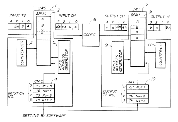
Figure 6 shows the outline of the first preferred
embodiment of the present lnvention. A digital exchange system
shown in Figure 6 comprises a primary time switch (SWO) 1, a
speech path memory (SPMO) 2, a write counter (CTO) 3, a control
memory (CMO) 4, a read address generator 5, a codec (CODEC) 6, a
secondary time switch (SW1) 7, a speech path memory (SPM1) 8, a
write address generator 9, a control memory (CM1) 10, and a read
counter (CT1) 11.
The first embodiment of the present invention handles a
basic-rate of 64kbps, and a sub-rate of 32kbps. However, the
present invention is not limited to these bit rates, but includes
sub-rates of, for example, 16kbps or 8kbps with respect to the
64kbps basic-rate.
It is now assumed that an input time slot signal ("INPUT
TS") which is input to the primary time switch 1 includes plural
(two) respective time slots including basic-rate signals A and B,
and a single time slot commonly including a plurality (two) sub-
rate signals "a" and "bn. The input time slot signal is
sequentially written into the speech path memory 2. During the
read operation of the speech path memory 2, a read time slot (time
slot to be read) is specified by time slot information written by
the software function of a controller (not shown) connected to the
control memory 4, and the position of each bit of each time slot
in the speech path memory 2 is specified by the read address
generator 5. The read address generator 5 generates addresses
specifying the bit positions so that the first four bits (data
"a") in input time slot "2" having the sub-rate signals "a" and
_ ~.
205?409
13 27879-79
"b" are read twice during a time corresponding to the input
channel number "2", and the second four bits (data "b") in the
input time slot "2" are read twice during a time corresponding to
the input channel number 3". In the above manner, an input
channel signal ("INPUT CH") shown in Figure 6 is output to the
codec 6.
The codec 6 receives the input channel signal from the
primary time switch 1 and executes coding (compression) and
decoding (decompression) procedures on the input channel signal.
Then, the codec 6 outputs an output channel signal ("INPUT CH"),
which is composed of a plurality of (two) identical (i.e., an
individual, corresponding) sub-rate signals in an identical
channel (e.g., AA in output channel "0") and a decoded
(decompressed) signal in one i.e., an individual, corresponding
channel (e.g., "a" in output channel "2").
The output channel signal is input to the secondary time
switch 7, and written into areas of the speech path memory 8
specified by the write address generator 9. During this write
operation, with respect to consecutive channels of the output
channel signal, each including the identical sub-rate signals (AA
in the output channel "0" and BB in the output channel "1"), the
write address generator 9 generates write addresses which makes it
possible to combine the sub-rate signals of the consecutive
channels "0" and "1" and place combined sub-rate signals in the
odd (last) channel (output channel "1") of the consecutive
channels. As shown in Figure 6, the sub-rate signals A and B are
written into the area of the speech path memory SPM1 corresponding
to the output channel "1".
14 2~52~9 27879-79
During the read operation of the speech path memory 8,
the channel numbers of the speech path memory 8 which are written
into the control memory 10 by the software procedure of the
controller (not shown) are sequentially read from the control
memory 10, and the position of each bit contained in each channel
is specified by the read counter 11. In Figure 6, the content of
the channel number "1" is read out from the control memory 10 in
the time slot "0" on the output side of the speech path memory 8,
and the contents of the channel numbers "2" and "3" are
respectively read out therefrom in the output time slots "2" and
"3".
Figure 7A shows the primary time switch (SW0) 1 shown in
Figure 6 in detail. As shown, the read address generator S shown
in Figure 6 is composed of a counter 50 and a ROM (Read Only
Memory) 51. An input time slot signal which is input to the
speech path memory 2 consists of 32 times slots, as shown in
Figure 8. The basic-rate signals (64kbps) are stored in the first
16 time slots, namely, time slots "0" - "15", and sub-rate signals
(32kbps) are stored in the second 16 time slots, namely, time
slots "16" - "31" in such a way that two 32kbps sub-rate signals
are combined and placed in one time slot. It will be noted that
the input time slot signal shown in Figure 8 is used in the
following description for the sake of simplicity, and the input
time slot signal processed by the present invention is not limited
to the input time slot signal shown in Figure 8.
The input time slots are written into the speech path
memory 2 in accordance with the addresses generated by the write
counter 3, which is driven by a clock signal having a frequency of
_.,,;
2~52409
27879-79
2.048MHz (=64k x 32 channels) or 8.192MHz (equal to an integer
multiple of 1.048MHz). Hereafter, 2.048MHz and 8.192MHz are
referred to 2MHz and 8MHz, respectively, for the sake of
simplicity. The output signal of the write counter consists of
five high-order bits (32 count numerals) indicating the time slot
position of the speech path memory 2, and the three low-order bits
(8 count numerals) indicating the bit position thereof.
The read operation of the speech path memory 2 will now
be described with reference to Figure 7B. The time slots are
sequentially read out from the speech path memory 2 in the order
of the read-side channel number, that is, "0", "1", "2", ... . In
Figure 7B, the input time slot number "0" on the write side of the
speech path memory 2 is supplied to the speech path memory 2 from
the control memory 4 during a time corresponding to the input
channel number "O". During this time, three bits "0", "1" and "2"
of the output signal of the counter 50 form a count numeral
generated by an eight-bit counter, as shown in (d) of Figure 7B.
The ROM 51 receives the bit "7" and bit "2" from the counter 50,
and generates a bit-2 signal, which is the same as the bit "2"
output by the counter 50 during a time when the first 16 channels,
that is, channels "O" - "15" are processed. During this time, the
bit "7" output by the counter 50 is maintained at a low level, as
shown in (b) of Figure 7B. Thus, as shown in (d) of Figure 7B,
the three low-order bits of the read address change so that it
increases one by one. That is, the eight-bits of each of the
channels "O" - "15" are sequentially addressed.
Meanwhile, when the time slot number "16" (input channel
"16") is read, the time slot number "16" on the write side is read
2052~9
16 27879-79
out from the control memory 4. At this time, the bit "7" output
by the counter 50 is switched to a high level, and the bit "2" is
maintained at "0" during a period corresponding to the eight-bits,
as shown in (c) of Figure 7B. Thus, the bits "O" and "1" of the
counter 50 and the bit "2" of the ROM 51 show bits "O", "1", "2"
and "3" in this order in each of the first and second halves of
one channel, as shown in (d) of Figure 7B. Hence, only the sub-
rate signal "a" written into a position corresponding to the first
four bits of the time slot "16" in the speech path memory 2 is
twice read out from the speech path memory 2, and the input
channel signal shown in ~f) of Figure 7B is obtained. The channel
"16" has two identical sub-rate signals "a".
During a time corresponding to the input channel "17",
the input time slot number "16" is read out from the control
memory 4, and input to the speech memory 2. During this
operation, the bit "2" of the ROM 51 is maintained at "1". Thus,
the address consisting of the three low-order bits applied to the
speech path memory 2 changes twice in the order of "4", "5", "6"
and "7", as shown in (d) of Figure 7B. That is, a pattern of "4",
"5", "6" and "7" appears twice during the input channel "17".
Thus, the sub-rate signal "b" written in a position corresponding
to the second four bits of the time slot "16" is twice read out
from the speech path memory 2. In the above manner, the two sub-
rate signals in each of the input time slots "16", "18", "20",
on the write side are placed in two different input channel (16,
17), (18, 19), (20, 21), ... . The input channel signal shown in
(f) of Figure 7B is input to the secondary time switch 7.
Figure 7C shows a decoding (decompressing) operation of
t
2052409
17 27879-79
the primary time switch (SW0) 1 shown in Figure 7A. For the sake
of simplicity, the input time slot signal consists of four time
slots.
The secondary time switch (SW1) 7 will now be described
with reference to Figure 9A. The write address generator 9 shown
in Figure 9A is composed of a counter (CT10) 90 and a ROM 91. The
output channel signal ("OUTPUT CH") which is output by the codec 6
has 32 channels, as shown in Figure 9A. Each of the first 16
channels "O" - "15" out of the 32 channels includes two identical
sub-rate (32kbps) signals such as AA or BB, and each of the second
16 channels "16" - "31" includes a basic-rate signal, such as "a"
or "b".
Figure 9B shows the operation of the secondary time
switch 7 shown in Figure 9A. The counter 90 counts the 2MHz (or
8MHz) clock signal, and generates bits "O", "1", "2" and "7", as
shown in (a) of Figure 9B. The other bits "3" - "6" are omitted
from Figure 9B for the sake of simplicity. The bits "0" and "1"
from the counter 90 are directly supplied to the speech path
memory 8, while the bit "2" and the bits "3" - "7" indicating the
channel number are supplied to the ROM 91. During the period when
the counter 90 has a count numeral which is any of the channels
"O" - "15" and an even channel is being processed, the ROM 91
generates an output signal which indicates an odd channel obtained
by adding +1 to the even channel, as shown in (d) of Figure 9B.
The output signal of the ROM 91 serves as the write address of the
speech path memory 8 (address of the channel number). When the
counter 90 has an odd channel, this indicates the channel number
to be accessed, while the bit "2" is changed to a bit "2'", as
18 2 0 5 2 4 0 9 27879-79
shown in (b) of Figure 9B. That is, when the counter 90 has an
odd channel prior to the channel "16", the bit "2" is maintained
at "1". When the counter 90 indicates an even channel ("0" r "2",
"4", ...), the bit "2'" is the same as the bit "2".
The output channel signal shown in Figure 9B from the
codec 6 is input to the speech path memory (SPM1) 8, and the eight
bits of the channel "0" in the output channel signal are
sequentially written into the area assigned to the channel "1" of
the speech path memory 8. The first four bits of the channel "1"
subsequent to the channel "0" are overwritten into the second four
bits (bits "4" - "7") of the area of the channel "1" two times, as
shown in (c) of Figure 9, because the bit "2'" from the ROM 91 is
"1". In this manner, the sub-rate signal A is written into the
first four-bit area of the speech path memory 8 related to the
channel "1", and the sub-rate signal B is written into the second
four-bit area thereof related to the channel "1".
Figure 9C shows a coding (compressing) operation of the
secondary time switch 7 shown in Figure 9A, in which a 64 kbps
signal is generated from the 32 kbps signals A and B. For the
sake of simplicity, the output channel signal consists of four
channels. Four periods, a,~,~, and ~ are defined as shown in (f)
of Figure 9B. During the period a, only the sub-rate signal A is
written into the first four bits of the eight-bit area of the
speech path memory 8 related to the address (channel) "1". In the
same manner as described above, the contents of the eight-bit area
specified by the address "1" are A/A, A/B and A/B during the
periods ~,~, and ~, respectively where A/A means that the first
four bits are A and the second four bits are A. During the period
:
18a 2 0 5 2 4 0 9 27879-79
~, the sub-rate signals A and B are placed in one time slot on the
output side of the speech path memory 8. The signals of the
channels "2" and "3" are written into the area related to the
channels "2" and "3" of the speech path memory 8. In the above
manner, signals of up to the channel "15" of the output channel
signal are written into the speech path memory 8.
The signals of the channels "16" - "31" of the output
channel signal are written into areas related to the channels "16"
- "31" of the speech path memory 8, respectively.
Data is read out from the speech path memory 8 by
reading the contents of the control memory 10 in accordance with
the output time slot numbers. The contents of the control memory
10 are written therein by the software control procedure of the
controller 100 shown in Figure 9A. In Figure 9B, the contents of
the channel n 1" of the speech path memory 8 (the combined sub-rate
signals A and B) are read out from the speech path memory 8 during
the output time slot "0", as shown in (e) of Figure 9B. During
the time slot "1", no data is read out from the speech path memory
8. In this manner, the combined sub-rate signals are read out
from the speech path memory 8 by reading the contents of the
control memory. During the output time slots 16 - 31, the
contents of the areas of the speech path memory 8 related to the
channels 16 - 31 are read out from the speech path memory 8,
respectively.
It is also possible to write the sub-rate signals in the
even channel numbers of the speech path memory 8 by reading the
contents of the control memory.
A description will now be given of a second preferred
~ '
2052409
18b 27879-79
embodiment of the present invention. The second embodiment of the
present invention handles a basic-rate signal having a bit rate of
64kbps and a sub-rate signal having a bit rate of 16kbps which is
a quarter of the basic bit rate.
Figure lOA shows a primary time switch used in the
second embodiment of the present invention. The structure shown
in Figure lOA is different from that shown in Figure 7A in that
the input time slot signal which is input to the speech path
memory 2 includes time slot "16" in which four sub-rate signals
"a", "b", "c" and "d" are combined and such a time slot is
included for every four time slots, such as "20" and "24".
Further, in order to read each of the four sub-rate signals, the
read address generator 5 (Figure 6) is composed of the counter 50
and a ROM 52.
The operation of the primary time switch shown in Figure
lOA is shown in Figure lOB. An input time slot signal shown in
Figure lOA is input to the speech path memory 2. When the channel
"16" of the input channel signal on the read side of the speech
path memory 2 is specified during the read operation, the time
slot "16" on the write side (in which the sub-rate signals "a" -
"d" are written) is specified by the control memory 4. At this
time, bits "1", "2" and "7", out of the bits output by the counter
50, are input to the ROM 52, which generates bits "1'" and "2'",
as shown in (b) of Figure lOB. Thus, by the three low-order bits
of the read address of the speech path memory 2, bits "O" and "1"
of the time slot 16 (two bits of the sub-rate signal "a") are
repeatedly (four times~ read out from the speech path memory 2, as
shown in (c) and (e) of Figure lOB.
, ,,
2052409
18c 27879-79
While the channel "17" of the input channel signal is
specified, the control memory 4 specifies the time slot "16" in
the same way as described above. During this time, the three low-
order bits includes bit "1'" which is set to "1". Thus, bits "2"
and "3" of the time slot 16 (two bits of the sub-rate signal "b")
are repeatedly read out from the speech path memory 2, as shown in
(c) and (e) of Figure lOB.
In the same way as described above, the sub-rate signals
"c" and "d" are read out from the speech path memory 2 when the
channels "18" and "19" of the input speech signal are specified.
As a result, the sub-rate signals "a", "b", "c" and "d" are
respectively read out from the speech path memory 2 during the
channels "16", "17", "18" and "19" of the input speech signal.
Figure llA shows the structure of a secondary time
switch used in the second embodiment of the present invention, and
Figure llB shows the operation of the secondary time switch shown
in Figure llA. The write address generator is composed of the
counter 90 and a ROM 92. The sub-rate signals A - D are
positioned in the channels "0" - "3" of the output channel signal,
as shown in (b) of Figure llB. During the time when the sub-rate
signals A - D are written into the speech path memory 8, the write
address (including bits "1'" and "2'"), which is the same as the
read address shown in Figure 10A, is generated by the ROM 92. In
this case, the write position of the speech path memory 8 in which
the contents of the channels "0" - "3" of the output channel
signal are written is the channel number "3" of the speech path
memory 8 (ROM 92 generates odd channel
,.~ ,...
- 19 - 2~52409
numbers which are separated from each other by four
channels, such as "7" and "11").
Thus, as shown in (d) of FIG.llB, the
identical sub-rate signals A of the channel "0" of the
5 output channel signal are repeatedly written
(overwritten) into the areas specified by bits "0" and
"1" of the channel number "3" of the speech path memory
8. The identical sub-rate signals B of the channel "1"
of the output channel signal are repeatedly written into
10 the areas specified by bits "2" and "3" of the channel
number "3" of the speech path memory 8. In the same way
as described above, the identical sub-rate signals C of
the channel "1" of the output channel signal are
repeatedly written into the areas specified by bits "4"
15 and "5" of the channel number "3" of the speech path
memory 8, and the identical sub-rate signals D of the
channel "1" are repeatedly written into the areas
specified by bits "6" and "7".
During the read operation of the secondary
20 time switch shown in FIG.llA, the sub-rate signals A - D
written into the area specified by the channel number
"3" of the speech path memory 8 are sequentially
specified by the control memory 10 during the time slot
"0" of the output time slot signal. In this manner, the
25 output time slot signal shown in (e) of FIG.llB is
obtained.
It is possible to write an area of the speech
path memory 8 corresponding to one of the channel
numbers "0", "1" and "2" instead of channel number "3".
30 It is also possible to handle an 8kbps sub-rate signal
in the same way as described above.
FIG.12 shows a third preferred embodiment of
the present invention. A write address generator 130
controlled by the control memory 4 is provided on the
35 input (write) side of the speech path memory 2 of the
primary time switch 1. The contents of the time slots
of the input time slot signal are written into the
2 0 5 2 4 0 9 27879-79
speech path memory 2 in accordance with addresses generated by the
write address generator 130. The contents of the speech path
memory 2 are sequentially read out therefrom in accordance with
addresses generated by a counter ("CTO") 150 provided on the
output (read) side of the speech path memory 2. A counter ("CT1")
190 is provided on the input (write) side of the speech path
memory 8 of the secondary time switch 7. The contents of the
channels of the output channel signal from the codec 6 are
sequentially written into the speech path memory 8. A read
address generator 210 controlled by the control memory 10 is
provided on the output (read) side of the speech path memory 8.
The contents of the speech path memory 8 are read out therefrom by
addresses generated by the read address generator 210.
Figure 13A shows the primary time switch 1 shown in
Figure 12. As shown, the write address generator 130 shown in
Figure 12 is composed of a counter (CTO1) 131, a ROM 132, an AND
gate 133 and an adder 134. Bits "O" and "1" of the counter 131
are directly input to the speech path memory 2. Bit "7" of the
counter 131 is input to the ROM 132, which generates bit "2". The
AND gate 133 receives bits "2" and "7" of the counter 131. An
output signal of the AND gate 133 is maintained at "O" during each
of the channels "O" - "15" of the input channel signal, as shown
in (f) of Figure 13B, which shows the write timings. Further, the
output signal of the AND gate 133 is maintained at "O" during the
first half of the period of each of the channels "16" - "31" and
maintained at "1" during the second half thereof. The output
signal of the AND gate 133 is input to the adder 134, which adds
the received output signal of the AND gate 133 to the channel
_ ~.
2052409
20a 27879-79
number of the input channel signal generated by the control memory
4, as shown in (g) of Figure 13B.
During each of the channels "0" - nl5", the channel
number of the input channel signal read out from
,:,
-21- 2a52409
1 the control memory 4 passes through the adder 134 and is
input to the speech path memory 2 . During the first
half of the period of each of the channels "16" - "31",
the adder 134 outputs the channel number of the input
5 channel signal read out from the control memory 4 to the
speech path memory 2, and during the second half
thereof, the adder 134 outputs to the speech path memory
a channel number obtained by adding +l to the channel
number of the input channel signal read out from the
control memory 4. Thus, the sub-rate signals "a" and
"b" stored in the time slot "16" of the input time slot
signal are respectively written into the first half of
the channel "16" of the input channel signal and the
first half of the channel "17" thereof.
FIG. 14A shows the secondary time switch shown
in FIG. 12 . The counter 190 outputs bits "O" - "7" to
the speech path memory 8. Thus, the output channel
; signal from the codec 6 is sequentially written into the
speech path memory 8. The read address generator 210
20 shown in FIG.12 is composed of a counter (CT10) 211, an
inverter 2 12, an AND gate 213 and an adder 2 14. During
the read operation, the sub-rate signals placed in
different channels, such as A and B, are placed in an
identical time slot of the output time slot signal. Bit
25 "7" of the counter 211 is input to the inverter 212,
which outputs an inverted version of the bit "7" to the
AND gate 213, which also receives bit "2". Bits "O" -
"2 " are directly input to the speech path memory 8. An
output signal of the AND gate 213 changes, as shown in
30 (d) of FIG.14B. The output signal of the AND gate 213
is related to the sub-rate signals. As shown in (d) of
FIG. 14B, during the first half of the period of each of
the channels "O" - "15", the AND gate 213 outputs "O",
and during the second half thereof, the AND gate 213
35 outputs "1". During the period of each of the channels
"16" - "31", the output signal of the AND gate 213 is
maintained at "O".
- 22 - 2~ 2~09
1 The adder 214 generates the read address of
the speech path memory 8. During the period of each of
the channels "16" - "31", the channel number read out
from the control memory 10 passes through the adder 214,
and is input to the speech path memory 8. As shown in
(e) of FIG.14B, during the first half of each of the
channels "O" - "15", the channel number from the control
memory 10 is input to the speech path memory 8, and
during the second half thereof, the speech path memory 8
receives a channel number obtained by adding +1 to the
channel number read out from the control memory 10.
Thus, the sub-rate signal A in the channel "O" is read
out during the first half period of the output time slot
"O", and the sub-rate signal B in the channel "1" is
read out during the second half period of the output
time slot "1".
In order to obtain the above-mentioned
operation, it is possible to use a combination of the
primary time switch used in the first embodiment and the
secondary time switch used in the third embodiment or a
combination of the primary switch used in the third
embodiment and the secondary switch used in the first
embodiment.
The present invention is not limited to the
specifically disclosed embodiments, and variations and
modifications may be made without departing from the
scope of the present invention.