Note: Descriptions are shown in the official language in which they were submitted.
-1- 2Q52500
FIELD OF THE INVENTION:
This invention relates to a communication
system within a PABX, central office, computer, etc. for
transferring data between peripherals and a main
processing control, and has particular advantage for use
in distributed PABX systems.
BACKGROUND TO THE INVENTION:
Modern ISDN compatible PABXs typically use a
main central control and peripheral interface circuits,
for example the PABX type SX2000~ sold by Mitel
Corporation. Each peripheral interface circuit has a
controller which controls various peripherals such as
line interface circuits, network interface circuits,
etc. The various peripherals communicate with the
interface circuits using for example 2B + D, 23B + D or
30B + D line format protocol, the D-channel typically
operating at 16 kb/s or 64 kb/s. The peripheral
interfaces typically use common channel packet based
signalling over the D-channel, such as LAPD (Link Access
Protocol for a D-Channel), LAPB (Link Access Protocol,
Balanced), MiLAP (Mitel Link Access Protocol), DPNSS
(Digital Private Network Signalling System), or DASS 2
(Digital Access Signalling System No. 2). The D-channel
data is transmitted using HDLC at 16 kb/s or 64 kb/s to
the peripheral control.
Therefore the system requires an HDLC framer
at both ends for every ISDN D-channel communication link
between the peripheral control and each external
interfacing peripheral. With this architecture, the
peripheral controller requires significant amounts of
memory and computing capability for the processing of
all the different link layer protocols as well as
translation before transmission to the main central
control in the system's specific communication protocol.
_L
-2- 205250o
SUMMARY OF THE INVENTION:
The present invention provides a high speed
communication link between the peripheral nodes and a
single multi-link access protocol controller with an
S integrated HDLC framer in a processor of the main
control complex. Each peripheral node contains a very
simple control that forwards all the HDLC C-channel data
packets from the peripherals to a single MLAP
controller, thus making the peripheral nodes small in
physical size, extremely flexible to new interfaces and
very portable. Accordingly it facilitates the efficient
distributed deployment of the PABX. Using the present
system, the PABX itself or other premises communication
system may be distributed around a building, using a
backbone high speed link. Peripheral nodes may be
located at various places in a building with peripherals
such as line, network interfaces and associated digital
telephones at locations as needed. They need not be
centralized, adjacent the main control complex, as is
now required. This facilitates the provision of a
building with a flexible communication system having
substantially reduced building wiring requirements, no
need for peripheral processors, large amounts of memory
at the peripheral levels, HDLC framers per every
interface, bulky packaging and complex power supplies.
Further, it allows growth or modification of
a single communication system by adding or replacing
peripheral nodes as premises communication requirements
change, which thus can be used to service the entire
building, or portions of the building, without requiring
extensive new wiring or modification of the wiring.
It also facilitates expansion or
modification of the communication system in a modular
manner and in a cost effective manner.
-
-3- 2052500
In accordance with the present invention,
the bit rate of transmission of HDLC formatted data is
changed from 16 kb/s or 64 kb/s to 2.048 mb/s and vice
versa. It multiplexes plural modified HDLC packets to
S one physical link that is terminated by an HDLC framer
inside the multi-link access protocol controller in the
main control complex or, from one MLAP processor
controller, many peripherals can be accessed and
controlled. The functions of the present invention are
transparent to the end-point HDLC framers and hence to
the link layer protocol, as well as to peripheral
software.
In accordance with an embodiment of the
invention, a switching system is comprised of line or
network interface circuits for connection to peripherals
and trunks, peripheral nodes for controlling groups of
line or network interface circuits, a main control and
switching apparatus, apparatus for transmitting data
between the peripheral nodes and the main control and
switching apparatus, including a high data rate bus
connected therebetween, apparatus in the peripheral
nodes for receiving data from the peripherals and/or
trunks and for adding in the data an identifier of a
peripheral node port address of the source of the data,
whereby the transmitting apparatus can transmit the data
with the port address to the control and switching
apparatus in order that the control and switching
apparatus can recognize the source of the data and route
the data accordingly.
In accordance with another embodiment, a
switching system is comprised of a main control and
switching apparatus, line or network interface circuits
and peripheral nodes to which the peripherals are
connected, apparatus for transmitting data packets
between the peripheral nodes and the main control and
2052500
switching apparatus, the peripheral nodes being
physically located at a remote location relative to the
main control and switching apparatus, and a high speed
serial data bus connecting the main control and
switching apparatus with the peripheral nodes, and a
single MLAP controller with integrated HDLC framer in
the main control and switching apparatus, and apparatus
for demultiplexing, multiplexing and arbitrating the
reception and transmission of data from and to the high
speed data bus to and from the HDLC framer in the
peripherals.
In accordance with another embodiment of
the invention, a common channel relay system is
comprised of a PABX having a main control complex,
peripheral nodes each for connection to peripheral units
(digital telephones, data terminals, trunks, etc.), a
multi-link access protocol (MLAP) controller which is
controlled by the main control, a packet relay
controller in each peripheral node, for transmitting and
receiving D-channel data to and from the peripheral
units, uplink and downlink digital communication links
connected between the packet relay controllers and the
MLAP controller for carrying the D-channel data, and
multiplexer-demultiplexer apparatus in the MLAP
controller for operating the links at a bit rate which
is a multiple of the bit rate of the packet relay
controllers, whereby the MLAP controller is shared
between plural packet relay controllers.
BRIEF INTRODUCTION TO THE DRAWINGS:
A better understanding of the invention will
be obtained by reference to the detailed description
below, in conjunction with the following drawings, in
which:
Figure 1 is a block diagram of a prior art
system,
-
~5~ 205 2500
Figure 2 is a block diagram of an embodiment
of the present invention,
Figure 3 is a block diagram of a packet
relay controller used in the present invention,
Figure 4 is an illustration of a prior art
data packet and of a data packet used in this invention,
and
Figures 5A and 5B form a block diagram of
another embodiment of this invention, the pages
containing those figures being assembled as shown in
Figure 5, and being referred to below together as Figure
5.
DETAILED DESCRIPTION OF THE INVENTION:
Turning first to Figure 1, a switching
system according to the prior art is illustrated. A
main processor 1 is connected to a main system bus 3 to
which a switching unit 5 is connected. The elements
described are generic, in that the processor 1 includes
associated memory and other well known ancillary
apparatus. Switching unit 5 can be a time division
switch, a space division switch, a combination, or
networks thereof, or some other kind of switching unit.
Peripherals such as telephone sets 7, 9,
computer terminal 15 and trunks 11 are connected to line
or trunk interfaces 17, and are controlled by peripheral
control circuits 13. The peripheral control circuits
are connected through communication links 2 to processor
1. In some systems the peripheral control circuits may
be connected directly to bus 3, depending on the form of
PABX which is used.
A representative form of PABX which uses the
architecture of Figure 1 is described in U.S. Patent
4,616,360 issued October 7th, 1986, to which the reader
is referred.
-
20525~
Telephone sets 7 are digital telephones, forexample SUPERSET 4DN~ those which incorporate a digital
network interface circuit (DNIC) sold by Mitel
Corporation as type MT8972, a description of which may
be found in the Mitel Semiconductor Data Book, 1991 and
which is incorporated herein by reference. Telephone
sets 9 and representative computer terminal 15 are well
known ISDN Basic Rate station apparatus which may be
used in an integrated services digital network (ISDN).
Trunks 11 are representative digital public network
trunks, ISDN trunks, etc. These peripherals communicate
with the line or trunk interfaces 17 using the well
known 2B + D, 23B + D or 30B + D line format protocol,
wherein the D-channel is a data channel operating at a
16 kb/s or 64kb/s rate.
The peripheral circuits control the data
received by line or trunk interfaces 17, under ultimate
control of processor 1 through a dedicated communication
link 2 to the peripheral controller 13. Since the D-
channel can be one of numerous standardized link layerprotocols (LAPD, DPNSS, DASS 2 etc.) and the link layer
protocol requirement is that each connection should
always be terminated by a HDLC framer, an HDLC framer 19
is provided for each ISDN C-channel or ISDN like
communication link between the peripheral controller
unit 13 and the external interfacing peripherals 7, 9,
15 and public network trunks. Accordingly, for example,
in a communication system in which there are 1500
peripherals, there would be 1500 separate channels and
1500 HDLC framers required at the peripheral control
level.
There are several problems that need to be
resolved for the prior art system when engineering of
the peripheral control is performed, involving processor
performance, memory requirements, and number of HDLC
2052500
channels required. The HDLC framers must handle both 16
kb/s and or 64 kb/s data rates. The handling of HDLC
framers is a very real time intensive operation for a
microprocessor, e.g. a type MC68020 processor operating
at 12.5 MHz can handle approximately eight 64 kb/s
channels of HDLC data and only thirty-two 16 kb/s HDLC
channels under full load. However, under light call
traffic the microprocessor is able to handle about ten
times more. The amount of memory required to support
several different protocols can be in the range of 2
Mbytes to 4 Mbytes. Also usually some additional
hardware is required for microprocessor performance
improvements, such as DMA channels to help move the data
within the peripheral control.
It will be realized that the prior art
systems engineering can be very challenging since a
peripheral control that handles ISDN Primary Rate trunks
will require only a few HDLC framers (one per 23B or 30B
channels) but will require high processor performance
because trunk utilization is very high, e.g. 36 CCS. On
the other hand if the same peripheral control were used
for controlling line interfaces e.g. digital telephones
which require significantly lower call traffic rates of
4 CCS, the number of lines that the controller has
processor performance for is significantly higher e.g.
288. to utilize the peripheral controller's full
performance capability it would have to be equipped with
288 HDLC framers. However, it is not practical to
handle 288 HDLC framers with one processor.
Therefore, systems engineers of prior art
systems have been designing peripheral control
architecture that is very hierarchical, e.g. a trunk
interface card only handles trunks and has all the HDLC
framer resources, the necessary memory and processor
performance. As well, different line interface cards
2052500
for each different type of telephone's requirements have
the necessary HDLC framer resources, the necessary
memory and processor performance. Each line or trunk
interface card was designed to handle peak call traffic
rate requirements. Statistical call traffic analysis
could not be done with this architecture at the line
interface level. With this architecture a processor
within the peripheral control 13 was used to control and
communicate between the processors that terminate the
link layer protocol on the trunk interface or line
interface cards. With this architecture a very
processor intensive and complex peripheral control unit
results, which requires large and complex packaging,
large power supplies and complex interconnect backplane
structures. Therefore the cost of communication systems
is high and restrictive.
The present invention solves this problem.
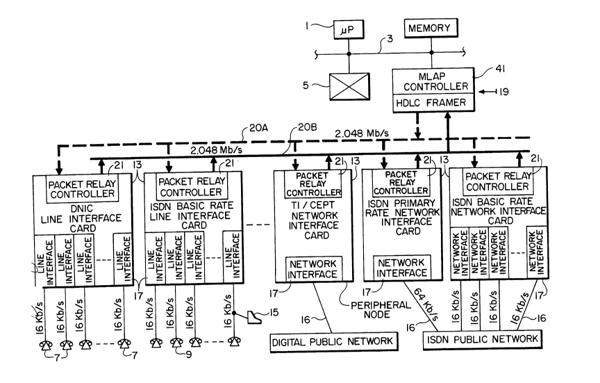
A basic block diagram of the invention will be found in
Figure 2. A preferably 2.048 mb/s data link, preferably
formed of optical fiber, is connected between a single
MLAP controller with integrated HDLC framer 41 and the
peripheral nodes 13. Each peripheral node is comprised
of a packet relay controller 21 and line or network
interface circuits 17. A block diagram of a packet
relay controller is illustrated in Figure 3. The form
of data packets in an HDLC frame and in a modified frame
as used within the present invention as carried on data
link 20A, 20B is illustrated in Figure 4.
Data is prepared by peripherals 7, 9, 15 or
by a network trunk 16 in HDLC format and is transmitted
to the line or network interface circuit 17 in the
appropriate line code. With reference particularly to
Figure 3, for data which is to be passed on the uplink
20B to the main control, HDLC format packets are
collected, which are received from the peripherals 7 in
.
~9~ 2052500
the D-channel, on line 23, (labelled ST Link From Line
Interfaces). The received data is passed into a DX
switch 25, preferably type MT8980 or MT8981 sold by
Mitel Corporation, which are described in the aforenoted
Mitel Semiconductor Data book and incorporated herein by
reference. The received data is passed from the DX
switch to serial to parallel converter 27, and then is
applied to parallel bus 29.
Microcontroller tprocessor) 31, using an
associated programmable read-only memory (PROM), which
may be a digital signal processor, tests each HDLC
packet for a flag octet ( 01111110 ). This, as may be
seen in Figure 4, forms the first octet of an HDLC frame
35.
Assuming that the processor 31 has detected
a flag octet, it stores the flag and following address,
control, information, CRC, and end of packet flag octets
in a memory 33 via bus 29.
Figure 4 illustrates a standard HDLC frame
format 35, which consists of start flag, address,
control, information, CRC, and terminating flag fields.
In the present invention, the HDLC frame
format is modified to that shown in 37. Between the
start flag and address, a port address identifier 39 is
inserted, which identifies from or to what port the
packet came from or is going to. The content of the
port address identifier is shown at 40. It is formed of
two octets, the first octet being a peripheral node
number identifier, which can identify up to 128
peripheral nodes addressed on one link. The first bit
"A" of that octet is an arbitration bit. If set to "1",
it identifies a request for access to that link. If set
to "0", it indicates that access to that link has been
granted.
-lO- 2052500
The second octet begins with a "1" followed
by 7 bits identifying the maximum number of port
addresses per peripheral node, in this case 128.
Returning now to Figures 2 and 3, as the
packet continues to arrive from the peripheral nodes,
the data is continuously tested by the microcontroller
31 for the terminating flag octet, so that the end of
the packet can be detected. Since HDLC is a bit
oriented protocol that inserts "O's" after strings of 5
"l's" in the data to prevent imitation of a flag or
abort character, the stored information in the memory
may not be octet aligned. It is for this reason that
the microcontroller must keep track of where the packet
ends.
The microcontroller 31 inserts the two byte
(octet) long port address identifier between the start
of packet flag and the HDLC frame address octet, as
shown in Figure 4. The two byte port address identifier
is used by the call processing element in the PABX to
identify where the packet came from. Since the first
byte in the port address identifier contains an access
arbitration bit (bit O) and a 7 bit peripheral node
address identifier (bits 1 - 7), it can address up to
128 peripheral nodes. The second address byte is used
to address up to 128 ports on that peripheral node, with
bit O being preserved.
The microcontroller performs O bit insertion
on the port address identifier, since it will be
received by an HDLC framer in the main control complex.
In addition, microcontroller 31 recalculates the CRC for
the packet that will be transmitted to the main control
complex. The packet is stored in memory 33.
The microcontroller then arbitrates for
access to the high speed uplink 2OB that carries packets
-11- 2052500
from the peripheral level to the main control complex.
The arbitration for access will be described below.
Once access has been obtained,
microcontroller 31 retrieves the stored packet 37 from
S memory 33 and forwards it including the flags at 2.048
mb/s to the main control complex.
However, prior to application to the uplink,
the packet 37 is converted to serial form in parallel to
serial converter 43, and flags are applied by flag
generator 45, in order to complete the modified frame
format 37.
The packet is received by a MLAP controller
41 which is programmed for non-protocol (non-LAPD)
packet reception mode of operation. Preferably that
controller is a type MC68606 controller, manufactured by
Motorola, Inc.
The port address identifier has compatible
bit assignment to the DLCI (data link connection
identifier) field for LAPD and is used by the MLAP
controller 41 to index to an external match table in an
associated memory to determine whether the port address
identifier has been assigned.
If the port address identifier is marked as
valid, the MLAP controller 41 uses address translation
tables in an associated memory to program a virtual DMA
channel for transferring the packet of information from
its HDLC front end framer into memory (not shown).
Reference is made to the Motorola, Inc. user manual for
a detailed description of the MC68606 controller
function, which is incorporated herein by reference.
For HDLC packets to be transmitted from the
main control complex to the peripherals, the MLAP
controller 41 programs its necessary registers for
transmission of the information. The port address
identifier is used for the address of the packet
L ~-
-12- 2052500
destination, the peripheral node and the port number.
MLAP controller 41 performs all the necessary functions
and transmits the D-channel packet to the peripherals at
2.048 mb/s. All the packet relay controllers 21 are
s connected to the down link 20A. The packet relay
controller 21 in the peripheral node 13 monitors the
data flow on the down link 20A, looking for an HDLC flag
octet.
The packet is received on the down link 20A,
and is converted to parallel format in serial to
parallel converter 43. The current address is detected
in address compare circuit 46, and O bits are detected
in O bit insertion detector 48.
Once a flag has been detected, the first
address octet is tested to see if the packet is
addressed to that peripheral node. If the packet was
addressed to the peripheral node or to the peripherals
that are connected to the line or network interface
circuit, then the complete packet is copied into buffer
memory 33.
The microcontroller 31 then tests the second
port address identifier octet to determine to which
peripheral device it is to forward the packet. The
microcontroller also recalculates the new CRC for the
packet, since the port address identifier octets have
been removed. Now the packet is ready for transmission
to the peripherals 7, 9, 15, etc. at the peripheral's
receive data rate, 16 kb/s or 64 kb/s. This is
performed by parallel to serial conversion in converter
47, applied to DX Chip 25 and transmission via the ST
link 49 to line or network interfaces circuit 17.
Arbitration of the data will now be
described with reference to Figure 5.
The up and down links 2OA and 2OB are
connected to optical fiber interfaces 52 each of which
-13- 205 2500
is comprised of an up link and a down link. The optical
fiber interfaces are interfaced at the main control
complex by optical fiber interfaces 53.
The up links from the fiber interfaces 53
S are connected to inputs of a multiplexer 55, the output
of which is connected to MLAP controller 41 with an
integrated HDLC framer.
Another output of multiplexer 55 is
connected to a request queue circuit 57, which has its
own control. The output of request queue 57 and of MLAP
controller 41 are connected to multiplexer 60.
Multiplexer 60 is connected to the down link input of
fiber interfaces 53, for transmission via the fiber 51
down links to down links 2OA.
The fiber links 51 form the building
backbone described earlier.
In operation, the arbitration is a request,
queue and grant system, and operates in the following
way for obtaining access to the up link. Access to the
down link is analogous. When the link is in an idle
state, the packet relay controller in the peripheral
node 13 arbitrates for access on the up link for
transmission of packets to the MLAP controller 41 in the
main control complex. Idle state is indicated by
continuous high logic state ("l's) on the up link for 15
or more bit intervals. When the up link is idle, the
packet relay controller can transmit a flag octet
followed by a card slot number with the first bit set to
"1" (high logic state), followed by a closing flag
octet. These three octets define a request packet that
is recognized by the multiplexer 55 and is pasted to the
request queue 57.
The packet relay controller also monitors
for access collisions on the link. The packet relay
controller monitors the up link when it is transmitting
2052500
the card slot number octet onto the link. If the
transmitted information is different from the receive in
the address compare circuit 46, it assumes that a
transmit collision had occurred.
S If a collision has been determined as having
occurred, the packet relay controller stops transmitting
for a period of time. The microcontroller 31 uses the
peripheral node address number for a delay count before
arbitrating for access to the up link again.
Upon determining that a collision has
occurred, The closing flag octet is not transmitted to
the multiplexer 55. The multiplexer 55 disregards any
request packets that do not have a closing flag.
If there was no collision, a request packet
is received by the packet relay handler 62 in a manner
to be described below.
The structure involving multiplexers 55 and
60, request queue 57 and packet relay handler control 58
and MLAP controller 41 is referred to below as a packet
relay handler 62. The packet relay handler uses the
start flag octet for byte alignment, if required. It
then tests the first bit of the card slot number. If
the first bit is set to "0", indicating a normal packet,
the packet is allowed to go through the multiplexer 55
to the MLAP controller 41. If, however, the first bit
is set to "1", indicating a request packet, a sequencer
within the packet relay handler copies that byte to the
request queue memory 57, which has a first-in first-out
structure.
The packet relay handler 62 does not allow
requests to be sent to MLAP controller 41; instead it
transmits idle bits or a normal packet to MLAP
controller 41 from a different peripheral node.
A control se~uence in the packet relay
handler 62 buffers all the peripheral node address
-15- 205 2500
numbers that are requesting access to the up link for
transmission of packets from the peripheral to the MLAP
controller 41. The priority is in sequence as the
packets are received by the packet relay handler 62.
S The request queue memory 57 should be of appropriate
size so that the estimated peak heavy traffic
circulation will not over-run. However if an over-run
does occur, the main control should be notified, and the
communication protocol recovers and retransmits any lost
packets.
The packet relay handler control 58 monitors
transmit and receive links to and from MLAP controller
41. When the packet relay controller 21 has finished
transmitting its packet, indicated by the closing flag
having been detected by the packet relay handler, a
request for access is pending in the request queue
memory. Then the packet relay handler control 58 looks
for an idle state on the link coming from MLAP
controller 41, as described above with regard to the
packet relay controller on the peripheral node 13. When
an idle state has been detected, the packet relay
handler 62 sends the top peripheral node address number
from the queue memory back to the packet relay
controller. The peripheral node address number being
sent back to the addressed peripheral node provide an
indication that it had received a grant for accessing
the up link, and that it can start transmitting its
packet once the link is free. The packet is then
transmitted by the packet relay controller 21 and has
the first bit of the peripheral node address number set
(logic "0") indicating to multiplexer 55 in the packet
relay handler that this a normal information packet and
that it should be routed to MLAP controller 41.
MLAP controller 41 interfaces to main
processor 1 memory through CPU bus 3 in the main control
-16- 2052500
complex in order to route the D-channel data to the main
control complex.
It has been determined that under heavy
traffic conditions a 1500 line PABX needs only about 2%
S of its available bandwidth of the communication system
described herein for call control. The remaining
bandwidth can be used for other data transport
functions.
A person understanding this invention may now
conceive of alternative structures and embodiments or
variations of the above. All of those which fall within
the scope of the claims appended hereto are considered
to be part of the present invention.