Note: Descriptions are shown in the official language in which they were submitted.
1
FORCE BALANCE INSTRUMENT WITH
ELECTROSTATIC CHARGE CONTROL
This invention was made with support under Contract .
No. F07~01-87-C-0065, awarded by the United States Air
Force Space pivision. The Government has certain rights
in this invention.
BackcZ~oun,d of the Inventian
The present invention relates to force balanced y
instruments of the closed laop type, and more particularly
concerns a force balanced instrument in which position of
1p a sensing mass is capacitatively sensed and the mass is
electrostatically forced toward a null position.
In a force balanced se~asing instrument, such as an
accelerometer for example, it is generally desirod that
the instrument out~u~t signal be prr~portional to the input
condition to be sensed. Therefore, i~a many types of
el.eat~ostatic and electromagnetic gorCe balanced sensing
instruments special techniques are resluired to obtain a
linear .relation bet~een the instrument output axed the
sensed input. In electrostatic and e7:cctromagnetic
20' instruments ttse forees applied by ~Che instrument forcer
are riot linearly relatedl tc the feedback voltage or
current supplied to the f~roer. Furthermore, for aptimum
operation of the instrument itself it is' preferred that
the feedback fore applied bywthe feedback contr~l network
have a la.near relatioa~ to 'the sensed'input. Thus, special
2
techniques have been employed for obtaining such
linearity.
For example, in an electrostatic force balanced
accelerometer of the type Shawn in U. S. Patent 4,679,434,
for Integrated Force nalanced Accelerometer, of Robert
Stewart, electrostatic forcing in a closed loop system is
employed to position and obtain an output from a pendulous
inertial mass. The electrostatic forcing system employs
a capacitative pickoff electrode on each side of a
peudulaus member that has been etched from a silicon
substrate. The electrodes also apply nominally equal and
opposite bias forces to the pendulous member to which is
applied a control voltage. Tn another control arrangement
for an accelerometer of this type, a fixed bias voltage
and feedback voltage are applied concurrently to pickoff
and forcing electrodes on opposite sides of the sensitive
mass. The arrangement is such that a net force on the
pendulous mass applied by this control system is the
difference between the two forces, which is effectively
proportional to the feedback voltages, because the fixed
bias voltage is a constant.
This system has a number of problems, including the
large negative spring effect associated with the required
fixed bias electrical fields. Even in the absence of any
input acceleration to be sensed, these bias fields are
required, and, since the bias field may vary; the
instrument may have poor null stability and poor
repeatability. In such systems many factors, such as gap
varistion, aging of components, temperature variations,
and the like provide sources of error that may result in
spurious output and decreased null stability. Potentially
this spurious bias error is a large error. Small
variations in eT~ctric field are exacerbated by the large
negative spring effect associated with voltage contro3. in
both parallel and non-parallel motion.
3
Accordingly, it is an object of the present invention
to provide a force balanced instrument that avoids or
minimizes above mentioned problems.
Su,~ma of the lz;~~er~t'~,on
In carrying out principles of the present invention
in accordance with a preferred embodiment thereof,
position of the sensing member of a force balanced sensing
instrument is controlled by generating a pickoff signal
indicative of displacement of the sensing member from a
null position, repetitively applying to the sensing member
a constant magnitude force, independent of displacement of
the sensing member, alternately for first and second
periods of time in respectively opposite directions. The
first and second time periods are varied in response to
the pickoff signal so as to effect a difference in the
first and second periods that results in a net force on
the sensing member equal and opposite to the applied
inertial farce, thereby maintaining the pickoff at null.
Thus, the difference between the periods is a linear
measure of acceleration of an accelerometer proof mass.
According to a feature of the invention, first and
second electrostatic plates mounted on opposite sides of
a movable sensing member cooperate with the sensing membez;
to form first and second capacitors respectively that, vary
oppositely as the member moves in response to an' input
that is to be sensed. Equal charges are applied to the
first and second capacitors fox successive time intervals
to establish first and second voltages on the respective
capacitors which force the s~nsang~ member toward null
position. The difference between the voltages on the
capacitors in successive time intervals indicates the
displacement o~ the sensing anember and may be employed to
contro3 the durat~ions of respec~i~e ~nes o~ the time
intervals so as to move the sensia~~ member toward'a null
position. Effectively, the system generates its pickoff
,:
4
signal by sensing the voltages that are associated with
the capacitor forcing charges.
Brief ~esc~.~lat~.on e_U~awznas
FIG. 1 is a block diagram of a force balanced sensing
instrument employing principles of the present invention;
FIG. 2 is a synchro-graph illustrating timing of
various operations of the system of FIG. 2;
FIG. 3 illustrates a modification of the circuitry of
20 FIG. 2;
FIG. 4 illustrates still another modification of the
circuitry of FIG. 1; and
FIG. 5 is a timing chart for the circuit of FIG. 4.
~7etailed Descriiption of the Invention
Schematically and functionally illustrated in FIG. 2
is an accelerometer, generally indicated at 20, which may
be of the type described in U. S. Patent 4,67,434. The
accelerometer includes a pendulous mass 22 and a pair of
electrostatic plates or electrodes 24,16 positioned close
to but slightly spaced from and on opposite sides of the
mass l2. electrostatic plates 14,26 form pickoff and
forcing plates. ~s described in detail in Patent
4,67,434, ~lae instrument cpmprises a central inertial
mass tlxat is etched from a semi-conductor substrate, such
as silicon. The inertial mass is attached to the
substrate by hinges, all of which are formed by
anisat~opic etching of the single crystal silicon so that
the mass is connected to the substr~.te in a cantilevered
arrangement to deflect about an instrument output axis in
response to acceleration along the input axis. The
inertial mass is provided pith electrically conducive
surfaces on oppos~ae s~:des theraof which are adjacent to
but spaced a~~ng, the input axis from electrically
conductive surfacea of plates l4; 16: In a three axis
inertial measurement unit, three or more aCCelerOmeterS of
5
the type illustrated in U. S. Patent 4,679,431, or
equivalent instruments may be employed.
According to the present invention, force balanced
control of the position of pendulous mass 12 is provided
by a method that controls charge on the capacitor plates
and causes the plates to simultaneously act as both
pickoff and forger elements. The arrangement eliminates
both the need for a separate pickoff excitation source and
the negative electrostatic spring effect associated with
the prior voltage control systems fox parallel plate
motion and significantly reduces the effect for non
parallel plate motion. Moreover, the method employs a
pulse width modulated rebalance implementation that
provides a digital output capability and improved
linearity.
xn general, the instrument is operated by
repetitively applying a constant attractive force, acting
alternately on opposing sides of the sensing mass. fihat
. is, a fixed force is applied first to one side for a part
of a cycle and then a force of the same magnitude is
applied to the other side for the remainder of the cycle,
and the cycle is continuously repeated. k'or parallel
. plates, the force is independent of the displacement of
the sensing amass. The fixed force is applied to one side
or the other for varying intervals. The relative lengths
of successive intervals ars determined by the magnitude of
acceleration experienced by the sensing mast. The
relative lengths of the successive intervals or part
cycles of application of force to alternatively opposite
sides of the pendulous mace are controlled by varying the
duty cycle of a periodic wave, such as a square wave.
Thus, if the dhty cycle is fifty percent, equal and
opposite forces are applied to the pendulum for equal
periods of time, ;and the average value of the resultant
force on the semsing mass is ~e~ro. The difference in
duration between the two portions of a single cycle is a
6
linear measure of acceleration. The period of this
difference can be used to gate clack pulses that are
readily interpreted as velocity increments, thereby
providing a digital output.
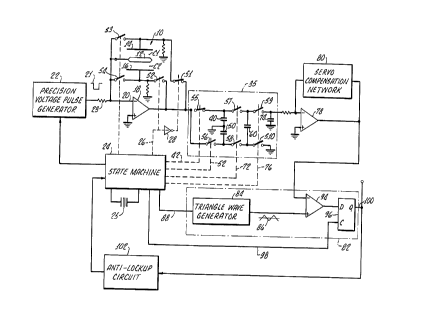
Referring again to FIG. 1, the plates 14, 16
cooperate with pendulous mass 12 to form capacitors C1 and
C2. The two capacitors are connected in two parallel
feedback paths of an operational amplifier 18 that
operates as a charge integrator. A first feedback path
runs from the amplifier output through a first switch S1,
through capacitor C1, to the amplifier inverting input at
point 20. A second feedback path includes a switch S2 and
capacitor C2, also connected to the input of the amplifier
at point 20. These switches may be field effect
transistors or other semiconductor switching elements.
Capacitor discharging or reset switches S3 and S4 are
connected across the respective capacitors C1, C2 for the
purpose of momentarily discharging these capacitors just
before each is charged. A precision voltage pulse
generator 22 includes a voltage reference that feeds a
voltage pulse 21 of precisely controlled voltage and
duration through a resistor 23 to the input of amplifier
Z8 when one or the other of switches S1, 52 is closed.
Switches S1 and S2 are closed alternatively by signals
from a stag machine 24 which provides timing aignals for
the system, including pulse generator 22, under control of
a 10 l~Iiz crystal 25. Plate select timing signals are fed
via a line 26 directly to ~2 and; via an invextor 28, to
S1 to insure that only one of the capacitors is charged at
a time.
The discharge switches S3 and S~ are operated
simultaneously for a shoat period of time, as indicated by
pulse 30 (FAG. ~) , beginning at a time tl, which is the
rise time of a duty cycle controlling sguare wave signal
32. Pulse 30 terminates at time ta. The timing of the
circuit allows a short period, such as 2.6 microseconds
7
far example, for the interval between t2 and t3 to allow
transition voltages to settle, and at time t, applies the
voltage charge pulse 21 of -2.5 volts with a duration of
3.2 microseconds to the input of the amplifier 18. The
charging pulse is applied to capacitor C1 through closed
switch S1. Switch S2 is open at this time. Switch S1
stays closed until the next reset time. The voltage an
plate 14, indicated at 36 in the synchro-graph of FIG. 2,
begins to ramp up at t3. At time t4, upon termination of
the charge pulse 21, the voltage on plate 14 remains fixed
until subsequent discharge is accomplished (assuming no
displacement of the mass).
A differential sample and hold circuit, generally
indicated at 35, alternately samples and stores voltage on
plates 14 and 16, respectively, in a first sampler stage,
and transfers each pair of samples to a differencing stage
of the sampler. The second stage of the sampler performs
a differencing function since each end of its storage
capacitor is alternately .referred to ground while being
charged by the previously sampled plate voltages. In this
way, very high common mode rejection is achieved, and the
second sample stage capacitor will be charged to a voltage
representing the difference between the two plate
voltages. The voltage on this capacitor indicates
deviation of the pendulum from the centerline between the
two plates. The third sampler stage transfers this
differential second stags voltage to another capacitor
referred to ground so that a single-ended signal results.
This signal is buffered, amplified, and connected to an
integrator stage with a ''bridged T°' servo compensation
circuit.
Details of the differential sample and held circuit
are illustrated within d~tted box 35 of FIG. 1. The
charge an capacitor C1 remains t~ provide an input to
amplifier 18. In the sample and hold circuit 35, the
amplifier output is sampled by closing a switch S5
connected between the amplifier output and a top plate
storage or sample device, capacitor 40. Closing of
sampling switch S5, under control of a timing signal on a
line 42 from state machine 24, occurs at time is (FIG. 2),
which is the time of initiation of a sample pulse 44 for
sampling plate 14.
At the end of the first part cycle of the duty cycle
of control square wave 32, which occurs at time t6,
switches S3 and S4 are momentarily closed to again
discharge both capacitors, and shortly thereafter, between
times t~ and te, switch S2 is closed, and pulse generator
22 provides a precision voltage pulse 21 to capacitor C2.
At the beginning of charging pulse 21 of this part cycle
capacitor C2 begins to charge up as indicated at wave form
48 of FIG. 2 to a voltage level determined by the charge
pulse applied from the output of amplifier 18 and the
capacitor gap. The capacitor voltage remains at this
level (again assuming no displacement, of mass 12) until
the end of this second part cycle of the duty cycle
controlling square wave which occurs at time t1o~
Shortly after time to when the lower plate 16 has been
fully charged, a second sample switch S6 is momentarily
closed to store the voltage on the lower plate 16 of
capacitor C2 in a second sample storage capacitor 50.
Switch S6 is clased under control of'a timing signal on a
line 52 from the stake ~aachine 24; This sampling of
voltage on plate 16 begins at a tame t9 shortly after tae
te~°mination of the charging pulse for capacitor C2:
Sampling of voltage on plate 14 is effected by sampling
the output of amplifier 1~ while capacitor C1 is charged
and while capacitor C2 is discharged Similarly, voltage
on plate 16'is sampled by sampling the output of amplifier
18, as indicated by pulse 45 of FTG. 2, in tie second part
of the cycle, after both capacitors C1 and ' C2 Crave been
discharged (at tb) and after ca~aciaor C2 has been charged
(te)
~~~~'~~~
wring the charging of capacitor. C1, second sampler
stage switches S7 and S8 are closed simultaneously, as
indicated by pulse 56 of FIG. 2, to transfer the stored
voltages of plate 14, capacitor C1, and plate 16,
capacitor C2, to opposite sides of a capacitor 60, which
foams the sampler difference storage stage. Switches S7
and S8 are closed by a timing pulse on a line 72 from the
state machine.
Accordingly, difference stage capacitor 60 stores a
signal proportional to the difference between voltage on
capacitor C1 when it was charged and the voltage on
capacitor C2 when it was charged.
From the preceding description it will be seen that
a precision pulse applied to charge integrator input 20
causes a known current to flow into the integrator for a
precise and known time duration. This pulse alternately
establishes a charge an each plate which causes the plate
to remain at a voltage determined by the quantity of
charge infected and the capacitance between the sensing
mass and the respective plate. The charge infected to
each plate remains constant from cycle to cycle, and, .
therefore, the voltage of the capacitor is a function only
of the accelerometer plate capacitance, which in turn
varies as the sensing mass l2 is displaced. Accordingly,
the voltage on each capacitor C1, C2 is a functi~n of
accelerometer sensing mass displacement and is used to
indicate sensing member position. However, the charge is
applied to only one plate at time, and thus the plate
voltages are sampled, than dif~er~r~ced to provide the
pickoff signal as the difference betw~er2 the sampled
v~ltageso
As described above, the stored samples are sent to
the difference sample capacitor 60, which accordingly
stores a signal r~pxesentative ~f sensing member
displacement. The differe~ace signal is sent at times
indicated by pulse "70 of F1G. 2 to the third sample stage
10
capacitor 74 via switches S9, 510, which are
simultaneously closed by a timing signal on a line 76 from
the state machine. The difference signal from capacitor
74 is fed to an integrating amplifier 78 at the output of
which appears an analog output representing the force
required to keep the pendulum at null position.
Integrating amplifier 78 is provided with a servo
compensation network 80 between its output and input. The
output of integrating amplifier 78 is fed to a pulse width
modulation circuit indicated in dotted box 82, which
provides the variable duty cycle controlling square wave
32. The duty cycle of square wave 32 is varied in
accordance with the pickoff signal from the integrator
amplifier 78.
Pulse width modulation circuit 82 comprises a
triangle wave generator 84 that produces a triangle wave
86 under control of a 10 khz clock signal received on a
line 88 from the state machine 24. The triangle wave 86
is compared with the position pickoff signal from the
output of integrating amplifier integrator 78 in a
comparator formed by an operational amplifier 94 that
receives the triangle wave 86 and pickoff signal at its
inverting and non-inverting inputs respectively. The
comparator output is used to trigger a flip flop 96 which
is clocked by a 2.5 M~dz clock signal supplied on a line 98
from the state machine. The output of the flip flop, on
a line 100, provides the pulse width modulated signal 32
(FIG: 2) and is fed through an anti.°lockup circuit 102 t~
the state machine. T3~is signal 32 is effectively
quantiti~ed because of the clock ,input to flip flop on
line 9~. Anti-lockup circuit 102 is comprised of a pair
of flip flops (not shown) connected to have mutually
exclusive states so as to prevent high frequency
comparator oscillations o~ a start up state
f~omretriggerir~g he Mate machine until it completes at
least a minimum cycle>
11
Illustrated in FIG. 3 are portions of a circuit for
providing electrostatic forcing and voltage pickoff, as in
the arrangement of FIG. 1, but utilising passive
switches,(e.g. diode steering) for charging the capacitive
plates of the sensing mass. ~1s shown in FIG. 3, the
sensing mass 12 and plates 14,16 forming capacitors C1 and
C2 respectively, are the same as illustrated in FIG. 1 and
previously described. In this case the constant current
source provided by the integrating amplifier 18 receives
precision voltage pulses at its inverting terminal 20
which are alternately positive and negative, but of the
same amplitude. Thus, instead of employing series
switches to steer the charging current pulse from the
integrating amplifier 18 to the respective plates 14,16,
diodes 110 and 112 are employed, respectively coupled in
the feedback paths from the output of amplifier 18 through
the capacitors G1 and G2 bank to input terminal 20 of the
amplifier. This arrangement avoids problems, such as
stray capacitances, that may be introduced by presence of
switches S1 and S2 in series with the capacitors C1 and
C2. Spurious charge that would be introduced by active
series switches, as when they are turned on, is avoided by
use of the passive steering diodes.
To provide a bipolar precision voltage pulse to the
integrating amplifier 18 there is employed an operational
amplifier 114 having a feedback from its output to its
inverting input and having a precision constant vol~.age
input to its non-inverting input provided from a voltage
reference 116 via a precision resistor 118. The none
inverting input terminal 120 of amplifier 17.4 is normally
held to ground by a M~7SFET transistor 122 which has its
gate controlled by a signal on a line 124 from the state
machine (not shown in FIG> 3) which provides overall
timing signals for the saveral elements as previously
described in connection with the embodiment of SIG. 1.
Transistor 122, when momentarily icurned of.f for generation
12
of a charging pulse, effectively provides a positive going
pulse at the non-inverting input to amplifier 114 and a
positive going voltage pulse at its output which is
applied via resistors 126, 128 to bath inverting and non-
inverting inputs of an operatianal amplifier 130. A
MOSF~T transistor 132 has its drain connected to the non-
inverting input 134 of amplifier 130 and its gate
controlled by a signal on a line 136 from the state
machine. When the transistor 132 is turned on the non-
inverting input 134 of amplifier 130 is pulled to ground
and the amplifier acts as an invertor, providing a
negative going pulse at its output. When transistor 132
is off amplifier 130 acts as a follower to provide a
positive going output pulse. These pulses of opposite
polarity are provided for the respective alternate charge
times of capacitors C1 and C2 according to the signal on
line 136 provided by the state machine. When a negative
precision pulse is provided at the output of amplifier 18,
capacitor C1 is charged through diode 110, and when the
positive charge is provided at the amplifier output the
capacitor C2 is charged through diode 112. Oppasite
polarity PNP and NPN transistors 140 and 7.42 respectively
are connected across the respective capacitors C1 and C2
and receive discharge timing signals via RC networks
144,146 on lines 148 and 150, respectively, from the state
machine. Thus, the accelerometer capacitors are
discharged, as previously described in connection with
FIO. 1. In this case, howeve~c, opposite polarity
transistors are required because o~ the oppasite polarity
charges applied to the respective capacitors.
Standard sample and h~ld circuits 7.52 and 154 have
inputs respectively connected to plate l4 of capacitor C1
., and plate 16 of capacitor C2. The sample and hold
circuits are respectively triggered by sample timing
signals received on line 156 and 158, respectively, fram
the state machine. The sample and hold circuit 3.52
13
samples and stores the negative voltage on plate 14, while
the positive voltage on plate 16 is sampled and stored by
circuit 154. Outputs of the two sample and hold circuits
are summed in a summing amplifier 160, having a resistive
summing network 162, 164 at its inverting input terminal.
Summing of the two opposite polarity voltages provides an
effective substractian of the two magnitudes to yield the
pickoff signal at output terminal 166 of amplifier 160,
which is fed to the servo compensation amplifier 178 of
FIG. 1 and to the pulse width modulator arrangement
illustrated in dotted box 82 of FIG. 1. The use of
standard sample said hold circuits receiving and sampling
opposite polarity plate voltages allows the use of the
summing amplifier 160 with its input referred to ground,
thereby avoiding common mode voltage errors that may be
present in a differential amplifier.
Still another arrangement presently preferred for
charging the accelerometer capacitors and sensing the
pickoff voltage is illustrated in FIG. 4. In the
arrangement of FIG. 4, like the arrangement of FIG. 1,
only a single polarity charging pulse is employed. only
one reset switch is needed, and steering switches for the
capacitors are referred to ground.
In FIG. 4 he accelerometer capacitors are again
indicted,as C1 and C2, having plates l4 and l6 adjacent a
pendulous mass, which in this FIG. is ~laown as a plate 12
common to both capacitors Cl and C2. The two separately
shown but electrically connected plates 12 represent the
sensing mass which,-as previously described, is positi~ned
k~etween the twa capacitative plates 14 and 16.
Integrating amplifier 18, ~~ in he other embodiments,
provides a constant magnitrxd~ charging current for a'fixed
time. Tn this ease the current is of a sia~gl~ polarity
fir charring bathe of the capacitoxs, which- are again
connected, as in bpth previously described embodiments, i~
separate but paxallel feedback paths between the output
14
and input of the integrating amplifier 18. Each of the
feedback paths includes a resistor, such as resistor 210
and 212, connected in series between the amplifier output
and a respective one of capacitor plates 14 and 16.
Steering transistors 216, 218 of the same polarity type
have their emitters connected to ground and their
collectors respectively connected to the junctions of the
capacitor plates 14, 16 and the respective resistors 210,
212. Accordingly, when either transistor 216 or 218 is
turned on the associated capacitor of the accelerometer
has its plate grounded. The transistors are turned on for
the alternate charging times of the respective capacitors
by appropriate timing signals fed from the state machine
(not shown in FIG. 4) on lines 222, 224 through current
limiting RC networks 226, 228.
A timing chart related to the circuit of FIG. 4 is
shown in FIG. 5 and may be useful in following this
description of the circuit. The timing chart is described
further below.
A precision fixed. value voltage pulse of precise
duration is agplied to the inverting input terminal 230 of
amplifier 18 by a circuit including a precision voltage
reference 232, which feeds a precision fixed level voltage
pulse via a resistor 234, a capacitor 236 and an amplifier
input resistor 238 to the input of amplifier 18: A MCSFET
transistor 240, having its date controlled by a timing
signal on a line 242 from the sate machine, is
momentarily turned on to pull ~lr~wn the jun~tior~ of
resistor 234 and capacitor 236 to provide a nsc~ati~r~ g~ing
voltage pulse during the charging pulse tine. Eecause a
positive going ramp f~r the charging pulse ~a desired at
the output of integrating amp3.a.fier l8, it is necessary to
change the voltage pulse input from ground to a negative,
such as -10 volts., Accordiaxgly, a diode 244 is provided,
having its cathode connected t~ ground and its: anode
connected to the junction of capacitor 236 and resistor
15
238. Thus, a negative going pulse, varying between 10
volts and ground at the junction of resistor 234 and
capacitor 236, is passed as a pulse at the amplifier input
that varies between ground and -14 volts. This pulse is
generated by the MpSFEr.C 240, which is momentarily turned
on by the control signal on line 242 from the state
machine to pull the junction of resistor 234 and capacitor
236 to ground. Because the duration of the pulse is much
less than the time constant of resistor 234 and capacitor
236, this negative going pulse is transmitted through the
capacitor and is level shifted to waxy between ground and
-10 by the action of diode 244.
The diode 244 may allow the pulse transmitted through
the capacitor 236 to rise slightly above ground.
Therefore, a transistor switch, such as a PFET 254 is
connected between ground and the junction of capacitor 236
and input resistor 238. The control eleo~trode of the PFET
254 is connected to a line 256 that sends a timing signal
from tine state machine to hald the junction of the
capacitor 236 and resistor 238 at ground (the PFET is on),
except when the desired voltage pulse oGCUrs. Thus, PFET
254 is normally on, to ground this junction, but is turned
off a very short time before occurrence of the pulse to
allow the negative going pulse to pass. The PFET is again
turned on a very short time after the termination of the
voltage pulse, thereby ensuring a ground potential at the
amplif~.er input 230 ix~ the absence c~f the v~lta~e pulse.
The negative voltage pulse provides a p~sitive going
ramp at the output of amplifier 18. S~.~ering transistors
216,218 of the accelerometer capacitors, when turned on,
will ground the plates 14, 16: dust before capacitor G1
is to, be charged, its steering tr~~~aator 27.6, which had
been in a conducti2ag state, is turned off to terminate the
grounding of plate' 7:4 and to allow the charging current
from the amplifier 18 to aharg~ capacitor C1. This causes
the voltage on the capacitor to ramp cap to the selected
16
value during the charging time. While the capacitor C1 is
being charged steering transistor 218 of capacitor C2 is
in a conducting state to ground plate 16 of this capacitor
sa that the current flowing from the output of amplifier
18 will in part flow through the resistor 212 and
transistor 218 to ground, thereby not affecting the
feedback currant through the charging capacitor C1.
Conversely, dust before capacitor C2 is to be charged its
conducting transistor 218 is turned off, and transistor
216 is conducting to ground capacitor Cl. Transistor 218
remains off until after the charging guise period has
terminated and a sample has been taken. Similarly, when
charging capacitor C2, its transistor 218 remains off
until after the charge time has been completed and a
sample has been taken. Transistors 216 and 218 are
switched on and off in mutually exclusive states,
although, if deemed necessary or desirable, both may be on
for the vary short periods prior to initiation of each
charging pulse and during the reset pulse (see FTG. 5) .
Reset (discharge) of both capacitors C1 and C2 is provided
simultaneously by a single transistor 260 that is
connected across both of the capacitors C1 and C2 and
operated by a reset timing signal on a line 262 from the
stag machine fed through a current limiting RC circuit
26~ . Preferably tFae very short xeset pulse is provided at
the initiation of each part cycle c~f the pulse width
modulated wave form from the circuit 98 of FTG. 2.
~n brc~er to generate the pickoff signal, charges on
the two capacitors C1 arad C2 are sampled by sample end
hold circbits generally indicated in dotted boxed 270 and
272, respectively. The two circuits are identical, and
only one need be e~cplained. A source fpllower in the form
Qg a ~OSFET 27~ has its gate connected via a resistor 276
to plate 1~ c~f capacitoar C1> Tts d~azn 278 i~ connected
to a suitable source ~f pos~.~ive potential and its source
280 is connected via a resistbr 282 to the drain electrode
17
of a controlling MOSFET 284 having its source grounded.
The gate of controlling MOSFET 284 is connected to receive
a timing signal on a line 286 from the state machine to
contxol the sample time and interval. The source of
MOSFET 274 is connected to one side of a storage capacitor
290, having its other side grounded. Resistor 276,
together with the input capacitance of the MOSFET 274
forms an RC circuit which limits any possible spike that
might be present. When MOSFET 284 is turned on the source
of MOSFET 274 is grounded through resister 282 and the
MOSFET 284, and it eats as a source follower to transfer
the voltage on capacitor C1 to the storage capacitor 290.
In this condition the source of transistor 2?4 tracks its
gate by the gate to source threshold of transistor 274.
When MOSFET 284 is off, no current flows, and storage
capacitor 290 is isolated, to thereby retain its charge.
Controlling MOSFET 284 is turned on solely during the
desired samplixzg time. The signal stored an capacitor 290
is fed through a MOSFET 291 that provides a low impedance
source to the inverting input of a differential amplifier
294.
The second sample arid hold circuit 272 is identical
to the first. Tt samples and holds the voltage on
capacitor C2, feeding the sampled v~ltage via a MOSFET 296
and a resistor 298 to a storage capacitor 299, ~rnd thence,
via a MOSFET 297 and a resistor 295,' to the non°i.nverting
input ~f differential ampl fier 294. The output of
d~ffereaxtial amplifier 294, on a line 30a, is fed to an
amplifier and remaining circuit w~zich m~~ be identical to
amplifier 7~ ans~ related circuitry shown in FIG. 1>
Sample and hold circuit 296 is crsntrolled by- a sample
t3,~ing pulse pxovided on a line 308 from the state
machine>
~n important acwan~age of the circuit illustrated in
FIB: 4 is tho fact that them aaee no ~~ritchi»g transistors
in series ~rith he output ~~ the int~~rating amplifier and
is
the capacitors Cl and C2e Further, only one discharging
transistor 260 is needed, thus eliminating the problems of
different stray capacitances and matching of the
transistors. Further, an improved circuit is employed for
generating the voltage pulse applied to the integrating
amplifier, and simplified sample and hold circuits are
employed.
FIG. 5 is a timing chart illustrating timing of
certain control functions of the circuit of FIG. 4e The
first line in FIG. 5, line (a) , shows the timing of the
pulse width modulator output. The next line (b), labelled
Discharge (reset), illustrates the time of occurrence and
relative duration of the reset pulse applied to the
discharging transistor 260. The next two lines (c), (d),
labelled as ground of plate 14 and ground of plate 16,
show the times of the grounding of these plates by the
conduction of their respective steering transistors.
Control of the PFET 254, shown in line (e), brackets the
charging time shown in the next line (f). Sampling times
for switches 1 and 2, namely MOSFET 284 and the
corresponding MOSFET of sample and hold network 2'~2, are
shown in lines (g) and (h) and the voltages on t$e
respective plates 14 and ~6 are shown in lines (i) and
(j). The durations of the reset pulse and charging time
periods and sampling pulses may be substantially the same
a~ stated in connection with the first described
embodiment of FIG. 9.a
Thud, it will be seen that no fixed bias (with its
resulting negative electrostatic spring effect) is needed
or employed because the f~rce balance is achieved by
controlling the duty cycle. The pulse width madulated
square wave 32, has a difference in its part periods that
is a linear measure of acceleration and can be used to
gate cl~ck pulses to provide a quantitized digital output.
Another significant ad~rantage of the described s~ste~n
is the fact that the capacitor plates t~ which are applied
19
fixed charges for selected periods of time perform a dual
Tale. The accumulated charge applied to the capacitors C1
and C2 establishes a net applied force on the pendulum
that is independent of gap ar sensing member position. on
the other hand, the voltage attained is a measure of the
gap, and the valtage difference between the opposing
plates is therefore used as the pickoff signal for the
force rebalance servoing of the system. Accordingly,
there is no need for a separate pickoff excitation supply.
l0