Note: Descriptions are shown in the official language in which they were submitted.
N~-362 - 1 - 20 528 1 1
~-~ TITLE OF THE INVENTION
IIETIIOD ~TD ARRU~G~I~ENT FOR DETECTING~ ~ ING BIT SEQUENCE
IN DIGITAL DATA COMMUNICATION~ SYSTEMS
BACKGROUND OF THE INVENTION
Field of the Invention
The present invention relates generally to a method
and arrangement for detecting a framing bit sequence in a
digital data communications system, and more specifically
to such a method and arrangement by which a plurality of
frame bit sequences can be rapidly detected and
communication established. The present invention is
concerned with a digital communications system wherein a
transmitted bit stream is divided into a plurality of
frames each of which is identified by a frame bit
sequence included therein. Each frame bit sequence
precedes data bit stream within the corresponding frame.
Description of the Prior Art
A circuit for detecting frame bit sequences is used
to establish synchronous condition between a data
terminal equipment and a user/network interface
interconnected by a two-wire transmission line (for
example). The user/network interface is usually attached
to an electronic exchange.
Before turning to the present invention it is
deemed preferable to discuss a known framing bit sequence
detecting arrangement with reference to Figs. 1 to 4.
Merely for the convenience of description, it is
assumed that: (a) each frame consists of 160 bits wherein
4 bits are assigned to a framing bit sequence, (b) the
time duration of one frame is 1 ms, (c) the framing bit
sequence is followed by data bits (viz., 156 bits) and
(c) consecutive frames transmitted are ascertained by
frame bit sequences "0000", "0001" , "0010", "0011",
"0100",
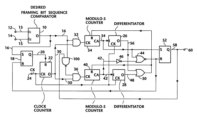
As shown in Fig. 1, a framing bit sequence
205281 t
comparator 10 is provided which has two input terminals 12,
14. The data bit stream 13 transmitted in a manner divided in
frames, is received at the input terminal 12, while a framing
bit sequence 15 is applied to the input terminal 14 for
detecting the framing bit sequence included in the frame
transmitted.
In the event that the comparator 10 detects a bit
sequence, included in a bit stream applied to the input 12,
which coincides with a framing bit sequence applied to the
input 14, the comparator 10 outputs a coincidence signal 16
assuming a high level (for example). The coincidence signal
16 is applied to a set terminal S of an RS flip-flop (FF) 18.
In this case, the FF 18 issues a reset signal 20 to a reset
terminal R of a clock counter 22. Thus, the counter 22 starts
counting clock pulses CK applied to the clock terminal CK
thereof via a terminal 24. The clock pulses CK are also
applied to a clock terminal CK of each of differentiators 26,
28. Timing charts of the operation of each of the
differentiators 26, 28 are shown in Fig. 3. Since the
operation of the differentiator 26 (28) is well known in the
art, further discussion will be deemed unnecessary.
The clock counter 22 issues a carry signal 30 which
assumes a logic 1 at the time when counting up 160 clock
pulses the number of which equals the number of bits of one
frame.
A modulo-5 counter 34, which follows an AND gate 32,
counts up if the signals 16 and 30 applied thereto assume a
logic 1 simultaneously. Another AND gate 36 is supplied with
-- 2
71024-172
205281 1
the coincidence signal 16 via an invertor 38 at one of the two
inputs thereof while receiving the frame count-up signal 30 at
the other input. This means that a modulo-5 counter 40 counts
up if the carry signal 30 from the counter 22 assumes a logic
1 and simultaneously the coincidence signal 16 assumes a logic
0. The operation of the modulo-5 counter 34 (40) is shown by
timing charts in Fig. 2.
In the event that the counter 40 counts up to the
maximum number thereof tviz., has counted from O to 4 in this
particular case~, the counter 40 issues a carry signal 42
(logic 1) at an output CA, which is applied to the
differentiator 28 and also to a NOR gate 44 via an invertor
46. An output 48 of the differentiator 28 assumes a logic 1
and hence resets the modulo-5 counters 34, 40 via an OR gate
50. Further, the output 42 resets a SR flip-flop 52 in this
case.
On the other hand, if the modulo-5 counter 34 counts
up from 0 to 4, it issues a carry signal (logic 1) 54 at an
output CA, which is applied to the differentiator 26 and also
to the NOR gate 44. An output 56 of the differentiator 26
assumes a logic 1 and hence resets the modulo-5 counters 34,
40 via the OR gate 50. Further, the output 54 sets the SR
flip-flop (FF) 52, which in turn issues a synchronization
detection signal 58 assuming a logic 1 indicating that
synchronization has been established.
The operation of the Fig. 1 arrangement will further
be described with reference to Fig. 4.
It is assumed that the comparator 10 detects a bit
71024-172
205281 ~
25 sequence "0000" in the bit stream 13 which coincides
with a framing bit sequence 15 assuming "0000" at a time point
A. Accordingly, the signal 16 assumes a logic 1. In this
instance, the carry signal 30 from the clock counter 22
remains to assume a logic 1 and, hence the state of the
counter 34 changes from 0 to 1. However, the counter 40
remains unchanged. Since the content of the framing bit
sequence 15 is advanced by one in response to a trailing edge
of the carry signal 30, the comparator 10 stores the next
framing bit sequence "0001" at a time point B. It is assumed
that the comparator 10 detects, at a time point C, a bit
sequence "0001" in the bit stream 13 which coincides with the
framing bit sequence 15 assuming "0001". In this case the
content of each of the modulo-5 counters 40, 34 remains
unchanged. Following this, the carry signal 30 from the clock
counter 22 assumes a logic 1 at a time point D and, hence the
counter 40 changes the state thereof from 0 to 1 in that the
coincidence signal 16 assumes a logic 0 at the time point D.
Similarly, the modulo-5 counter 34 changes the state
thereof from 1 to 2 at a time point E, after which it further
changes the state thereof from 2 to 3 at a time point H. On
the other hand, the modulo-5 counter 40 changes the state
thereof from 1 to 2 at a time point F, from 2 to 3 at a time
point G, and from 3 to 4 at a time point I. Since the
modulo-5 counter 40 counts up to the maximum number 4, the
counter 40 issues, at a time point J, the reset signal 42
which renders the counters 34, 40 to reset at a time point
slightly later than the time point J. Thus, each of the
-- 4
71024-172
205281 1
counters 34, 40 returns to the initial state (viz., 0) as
shown in Fig. 4.
In the event that the counter 34 returns to zero,
the framing bit sequence 15 again assumes "0000" and advances
the content by binary one in response to the trailing edge of
the carry signal 30 issued from the clock counter 22. It is
assumed that the comparator 10 detects a bit sequence "0000"
in the bit stream 13 which coincides with a framing bit
sequence 15 assuming "0000" at a time point K. Thus, the
signal 16 assumes a logic 1. In this instance, the carry
signal 30 from the clock counter 22 assumes a logic 1, so that
the state of the counter 34 changes from 0 to 1. However, the
counter 40 remains unchanged. Following this, it is assumed
that the coincidence signal 16 assumes a logic 1 at time
points L, M and N as illustrated in Fig. 4, and the
- 4a -
71024-172
205 2 8 1 1
NE-362 - 5 -
counter 34 counts up from 1 to 4.
At the time point P, which is approximately one
clock later from the time point N, a carry signal 54
assuming a logic 1 (denoted by numeral 70) is produced
by the modulo-5 counter 34. Accordingly, the
synchronization detection signal 58 assumes a logic 1 at
the time point P, indicating that a synchronization has
been established. After the time point P, the comparator
10 detects bit sequences "0100", "0101", ..., as shown in
Fig. 4. It is a usual practice to transmit meaningless
data following each framing bit sequence until the
transmitter is informed of the establishment of the
synchronization or until a time interval deemed
sufficient to establish the synchronization.
However, the above-mentioned prior art has
encountered the problem in that it takes an undesirably
long time until the reset signal 42 assumes a logic 1
(for example, at the time point J). In more specific
terms, it is extremely rare that the modulo-5 counter 34
counts up and allows the FF 52 to issue a logic 1 at an
early stage of initially operating the system.
Accordingly, it is highly desirable to retry the search
for the framing bit sequence by resetting the modulo-5
counters 34, 40. However, there is a high probability
that the comparator 10 will detect a bit sequence
included in the bit stream 13 which is not located at the
appropriate location, viz., the first 4-bit of each of
the frames. Therefore, in the event that the same bit
sequence erroneously detected at the comparator 10
appears at the same position of the following frames, it
takes a long time duration until the counter 40 counts up
and resets the modulo-5 counters 34, 40.
SUMMARY OF THE INVENTION
It is an object of the present invention to
provide a method of rapidly detecting framing bit
205 2 8 1 1
NE-362 - 6 -
sequences for establishing a synchronous condition in a
digital data communications system.
Another object of the present invention is to
provide an improved arrangement of rapidly detecting
framing bit sequences required for establishing a
synchronous condition in a digital data communications
system.
In brief, the above objects are achieved by a
method and arrangement wherein, in order to detect a
plurality of framing bit sequences for establishing
synchronization at a receiver in a digital
communications system, first and second counters are
rapidly reset in order to establish the synchronization
as early as possible. A comparator receives a bit stream
transmitted and a desired bit sequence for use in
detecting the framing bit, and compares the desired bit
sequence with part of the bit stream and issues a
coincidence signal in the event that the desired bit
sequence coincides with the part of the bit stream. The
first counter is coupled to receive the coincidence
signal, and allows an output indicating the
establishment of the synchronization to issue in the
event that it reaches a predetermined number of correct
coincidence signals. The second counter counts up the
number of occurrences of the output of a clock counter,
and resets itself and the first counter when reaching a
predetermine number of occurrences of a pseudo-
coincidence signal.
More specifically a first aspect of the present
invention is deemed to come in a method of detecting a
plurality of framing bit sequences for establishing
synchronization at a receiver in a digital
communications system wherein a bit stream is transmitted
to the receiver in a manner divided into a plurality of
frames each of which is identified by a frame bit
20528 1 1
sequence included therein, the method comprising the steps of:
(a) receiving the bit stream and a desired bit sequence whose
bit length equals a bit length of the framing bit sequence,
comparing the desired bit sequence with part of the bit
stream, and issuing a coincidence signal in the event that the
desired bit sequence coincides with the part of the bit
stream; ~b) issuing an output from a clock counter each time
the clock counter reaches the number of clocks corresponding
to one frame; (c) counting up the number of occurrences of an
event that the coincidence signal issues simultaneously with
the output of the clock counter at a first counter; (d)
counting up the number of occurrences of the output of the
clock counter at a second counter; (e) resetting the clock
counter and allowing the first and second counters to be
reset, in the event that the second counter reaches a
predetermined number; and (f) issuing an output which
indicates the establishment of the synchronization, in the
event that the first counter reaches a predetermined number.
A second aspect of the present invention is deemed
to come in a method of detecting a plurality of framing bit
sequences for establishing synchronization at a receiver in a
digital communications system wherein a bit stream is
transmitted to the receiver in a manner divided into a
plurality of frames each of which is identified by a frame bit
sequence included therein, the method comprising the steps of:
(a) receiving the bit stream and a desired bit sequence whose
bit length equals a bit length of the framing bit sequence in
a comparator, comparing the desired bit sequence with part of
-- 7
71024-172
2052 8 1 1
the bit stream, and issuing a coincidence signal in the event
that the desired bit sequence coincides with the part of the
bit stream and an enable signal is applied to the comparator;
(b) issuing an output from a clock counter each time the clock
counter reaches the number of clocks corresponding to one
frame; (c) counting up the number of occurrences of the
coincidence signal at a first counter; (d) counting up the
number of occurrences of the output of the clock counter at a
second counter; (e) resetting the clock counter and allowing
the first and second counters to be reset, in the event that
the second counter reaches a predetermined number; and (f)
issuing an output which indicates the establishment of the
synchronization, in the event that the first counter reaches a
predetermined number.
A third aspect of the present invention is deemed to
come in an arrangement of detecting a plurality of framing bit
sequences for establishing synchronization at a receiver in a
digital communications system wherein a bit stream is
transmitted to the receiver in a manner divided into a
plurality of frames each of which is identified by a frame bit
sequence included therein, the arrangement comprising: ~a) a
comparator for receiving the bit stream and a desired bit
sequence whose bit length equals a bit length of the framing
bit sequence, the comparator comparing the desired bit
sequence with part of the bit stream and issuing a coincidence
signal in the event that the desired bit sequence coincides
with the part of the bit stream; (b) a clock counter for
issuing an output therefrom each time the clock counter
-- 8
71024-172
205281 1
reaches the number of clocks corresponding to one frame; (c~ a
first counter being coupled to count up the number of
occurrences of an event that the coincidence signal issues
simultaneously with the output of the clock counter; (d) first
means heing coupled to the output of the comparator and an
output of the arrangement, the first means allowing the output
of the clock counter to pass therethrough except when the
output of the clock counter issues while the output of the
arrangement indicates the establishment of the
synchronization; te) a second counter being coupled to count
up the number of occurrences of the output of the clock
counter; (f) second means being coupled to reset the clock
counter and to allow the first and second counters to be
reset, in the event that the second counter reaches a
predetermined number; and (g) third means being coupled to
issue the output of the arrangement which indicates the
establishment of the synchronization, in the event that the
first counter reaches a predetermined number.
A fourth aspect of the present invention is deemed
to come in an arrangement of detecting a plurality of framing
bit sequences for establishing synchronization at a receiver
in a digital communications system wherein a bit stream is
transmitted to the receiver in a manner divided into a
plurality of frames each of which is identified by a frame bit
sequence included therein, the arrangement comprising: (a) a
comparator for receiving the bit stream and a desired bit
sequence whose bit length equals a bit length of the framing
bit sequence, the comparator comparing the desired bit
g
71024-172
20528 1 1
sequence with part of the bit stream and issuing a coincidence
signal in the event that the desired bit sequence coincides
with the part of the bit stream and an enable signal is
applied to the comparator; (b) a clock counter for issuing an
output therefrom each time the clock counter reaches the
number of clocks corresponding to one frame; (c~ a first
counter being coupled to count up the number of occurrences of
the coincidence signal: (d) first means being coupled to the
output of the comparator and an output of the arrangement, the
first means allowing the output of the clock counter to pass
therethrough except when the output of the clock counter issus
while the output of the arrangement indicates the
establishment of the synchronization; (e) a second counter
being coupled to count up the number of occurrences of the
output of the clock counter; (f) second means being coupled to
reset the clock counter and to allow the first and second
counters to be reset, in the event that the second counter
reaches a predetermined number; and (g) third means being
coupled to issue the output of the arrangement which indicates
the establishment of the synchronization, in the event that
the first counter reaches a predetermined number.
BRIEF DESCRIPTION OF THE DRAWINGS
The features and advantages of the present invention
will become more clearly appreciated from the following
description taken in conjunction with the accompanying
drawings in which:
Fig. 1 is a block diagram showing a known
arrangement for detecting framing bit sequences referred to in
-- 10 --
71024-172
2052 8 1 1
the opening paragraphs of the instant specification;
Figs. 2, 3 and 4 are timing charts which depict the
operation of the arrangement shown in Fig. 1;
Fig. 5 is a block diagram showing in block diagram
form, a first embodiment of the present invention;
Fig. 6 is a timing chart depicting the operation of
the arrangement shown in Fig. 5; and
Fig. 7 is a block diagram showing in block diagram
form a second embodiment of the present invention.
DETAILED DESCRIPTION OF THE
PREFERRED EMBODIM~NTS
Reference is now made to Fig. 5, wherein a first
embodiment of the present invention is shown in block diagram
form.
The first embodiment differs from the Fig. 1 prior
art in that: (a~ the arrangement of the former is provided
with a NAND gate 100 in place of the invertor 38 of Fig. 1,
(b) the output of the FF 52 is coupled to one of the two
inputs of the NAND gate 100 in lieu of the reset terminal R of
the FF 18, and (c) the output of the NOR gate 44 is coupled to
the reset terminal R of the FF 18. The remaining portions of
the Fig. 5 arrangement are the same as those of the Fig. 1
arrangement, and further descriptions will be omitted for the
sake of simplicity.
The first embodiment features an arrangement wherein
the carry signal 30 of the clock counter 22 does not fail to
count up the modulo-5 counter 40. Accordingly, the FF 18 is
reset at each time when the counter 40 issues the reset signal
-- 11 --
71024-172
20528 1 1
42.
The operation of the first embodiment will further
be discussed with reference to the timing chart shown in Fig.
6.
Similar to the case of the above discussed prior
art, it is assumed that the comparator 10 detects a bit
sequence "0000" in the bit stream 13 which coincides with a
framing bit sequence 15 assuming "0000" at a time point A, and
that the signal 16 also assumes a logic 1. In this instance,
the carry signal 30 from the clock counter 22 continues to
assume a logic 1 and, hence the state of the counter 34
changes from 0 to 1. Further, the counter 40 changes the
state thereof from 0 to 1. Since the content of the framing
bit sequence 15 is advanced by one in response to a trailing
edge of the carry signal 30, the comparator 10 stores the next
framing bit sequence "0001" at a time point B. It is assumed
that the comparator 10 detects, at a time point C, a bit
sequence "0001" in the bit stream 13 which coincides with the
framing bit sequence 15 assuming "0001". In this case, the
content of each of the modulo-5 counters 40, 34 remains
unchanged in the same manner as in the case of the above
discussed prior art. Following this, the carry signal 30 from
the clock counter 22 assumes a logic 1 at a time point D and
as a result the counter 40 counts up from 1 to 2 in that each
of the coincidence signal 16 and the synchronization detection
signal 58 assumes a logic 0 at this time point.
The modulo-5 counter 34 changes its state by
counting up from 1 to 2 at a time point E, while the modulo-5
- 12 -
71024-172
205281 1
counter 40 counts up from 2 to 3 at the time point E and then
from 3 to 4 at a time point F.
As a result of the modulo-5 counter 40 counting up
to the maximum number 4, the counter 40 issues, at a time
point G, the reset signal 42 which renders the counters 34, 40
to be reset at a time point slightly later than the time point
G. Thus, each of the counters 34, 40 returns to the initial
state (viz., 0) as shown in Fig. 6. It should be noted that
the counter 34 counts up at each time when the carry signal 30
assumes a logic 1.
In the event that the counter 34 returns to zero,
the framing bit sequence 15 again assumes "0000" and advances
the content by binary one in response to the trailing edge of
the carry signal 30 applied from the clock counter 22. It is
assumed that the comparator 10 detects a bit sequence "0000"
in the bit stream 13 which coincides with a framing bit
sequence 15 assuming "0000" at a time point H. Thus, the
signal 16 assumes a logic 1, and hence each of the counters
34, 40 changes the state thereof from 0 to 1. Following this,
it is assumed that the coincidence signal 16 assumes a logic 1
at time points J, K and L as shown in Fig. 6, then each of the
counters 34, 40 changes from 1 to 4.
At the time point M, which occurs approximately one
clock after the time point L, a carry signal 54 assuming a
logic 1 (denoted by numeral 102) is produced by the modulo-5
counter 34. Accordlngly, the synchronization detection signal
58 assumes a logic 1 at the time point M, indicating that
synchronization has been established. After the time point M,
- 13 -
71024-172
205281 1
the comparator 10 detects bit sequences "0100", "0101", ....
as shown in Fig. 6. As mentioned above, it is a usual
practice to transmit meaningless data following each framing
bit sequence until the transmitter is advised of the
establishment of the synchronization or until a predetermined
time interval deemed sufficient to establish the
synchronization, has lapsed.
As understood from the foregoing, the modulo-5
counter 40 counts up, without failure, in response to the
occurrence of the carry signal 30 from the clock counter 18.
This means that the issuance of the reset pulse 42 is
accelerated as compared with the prior art.
Experiments by the inventor have revealed that the
time required to establish synchronization can be shortened
from about 500 ms to approximately 100 ms, as compared with
the Fig. 1 arrangement, under the following exemplary
conditions: (a) each frame consists of 160 bits wherein 4 bits
are assigned to a framing bit sequence, (b) the time duration
of one frame is 1 ms, (c) the framing bit sequence is followed
by data bits (viz., 156 bits) and (c) consecutive frames
transmitted are ascertained by frame bit sequences "0000",
"0001" "0010", "0011", "0100", ......
Fig. 7 is a block diagram showing a second
embodiment of the present invention.
The arrangement of Fig. 7 differs from that of Fig.
5 in that: (a) the AND gate 32 of the latter arrangement
is omitted and the coincidence signal 16 is directly
applied to the counter 34 and (b) a desired framing bit
- 13a -
71024-172
2~5~8 1 1
sequence comparator 10' of the former arrangement is
similar to the counterpart 10 of Fig. 1 but modified to
accept an enable signal (viz., the carry signal 30~ at an
enable terminal E.
With this arrangement the comparator 10' is able to
output the coincidence signal 16 only when being enabled by
the carry signal 30. As clearly seen from Fig. 6, the
- 13b -
71024-172
~5~
NE-362 - 14 -
coincidence signal 16, which is issued in asynchronism
with the carry signal 30, is not used to induce either of
the counters 34, 40, to count up. Accordingly, it is
preferable to prohibit such unnecessary coincidence
signals from being issued by the comparator 10'.
In the above embodiments, a modulo-5 counter is
used. However, the present invention is by no means
limited to such usage.
While the foregoing description describes two
embodiments according to the present invention, the
various alternatives and modifications possible without
departing from the scope of the present invention, which
is limited only by the appended claims, will be apparent
to those skilled in the art.