Note: Descriptions are shown in the official language in which they were submitted.
CA 02052881 2000-11-24
VERTICALLY INTERCONNECTED
PARALLEL DISTRIBUTED PROCESSOR
Field of the Invention
This invention relates generally to computers and
more particularly to parallel distributed processors. More
specifically, the invention relates to a multi-layered,
vertically interconnected, parallel distributed processor
which allows the implementation of neural network computers
in which the degree of connectivity between individual
neurons thereof may be set and reset over a large dynamic
range resulting in a computer having the ability to learn
from, and adapt to, v<~rious data inputs.
Background of the Inveantion
Digital data processors operate a serial,
algorithmic mode and are capable of performing complex
calculations very accurately and quickly. Such processors
are incorporated in sEarial computers generally referred to
as von Neumann type machines and they implement data
manipulations in a stE~p-by-step fashion. Many information
processing problems can be solved by this approach,
particularly those requiring repetitive calculations;
however, von Neumann type computers perform inadequately
1
CA 02052881 2000-11-24
when doing tasks involving pattern recognition,
classification or associative learning. A further drawback
of von Neumann type computers is presented by the fact that
before a problem is amenable to solution, it must be fully
understood and reduced to a series of algorithms and the
algorithms must be translated into an appropriate language
for processing by a particular computer. Construction of an
appropriate algorithm for tasks involving interpretation of
patterns, particularly dynamically changing patterns such as
those encountered in speech recognition, high speed
character recognition and interpretation of moving scenery
present extremely dif:Eicult, if not impossible, tasks.
The brain of even a relatively simple organism
represents a data processor operating in a parallel,
distributed mode and it is capable of quickly and accurately
interpreting a large body of dynamically changing data
without the need for input of a complex algorithm. Such
operation is even more impressive in view of the fact that
signal propagation in the brain occurs at a speed many
orders of magnitude lower than the speed of propagation of
an electrical signal in a silicon chip. Biological neural
systems are characterized by a very high degree of
connectivity and signal processing is effected by both the
degree and architecture of these connections as well as
2
CA 02052881 2000-11-24
J~
their ability to be altered and reconfigured by specific
stimuli.
'Investigations of biological systems have led to
the development of ns:ural computing networks also termed
"parallel, distributed data processors." Such networks are
characterized by thEa presence of a large number of
individual computing elements typically termed "neurons,"
"unit cells," or "nodESS." These individual cells are each
interconnected to a plurality of other unit cells in a
complex network. Connections between pairs of unit cells
may be characterized ass weak or strong and also as excitory
or inhibitory. By the addition of the appropriate input and
output circuitry to one or more neural processors, a neural
network computer may be constructed. However, efforts made
heretofore to construct neural network computers have led to
complex software and have been hampered by inadequate
hardware.
Neural network computing systems are trained to
perform a particular task, rather than being programmed to
execute an algorithm. Training is accomplished by
configuring the pattern of connections between individual
neurons. Training may be done in a passive mode by simply
presetting the pattern, and in some instances the strength,
of the connections between individual unit cells so as to
elicit a desired response to a particular input. A more
3
CA 02052881 2000-11-24
sophisticated approach involves a dynamic method wherein the
actual output response of the network to a given input
signal is correlated with a desired output response to
generate a training signal which is then applied to the
network to reconfigure. the connections. A network of this
type is able to "learn" an appropriate response to a given
input stimulation. A dynamically trainable system can learn
from its mistakes and is capable of a large degree of self-
teaching.
While it geanerally agreed that the massively
parallel non-linear logic of neural network computers will
readily adapt them to a wide variety of practical
applications involving pattern recognition, speech synthesis
and the solving of multi-parameter problems, the actual
implementation of neural network information processing
systems has been hampered by a lack of appropriate computing
hardware. Presently, most investigations into neural
network computing sy~~tems are carried out by emulating
neural network systems on conventional von Neumann type
computers. While such simulation allows for testing of
particular neural network architectures, the conventional
digital computer, operating in a serial manner, inherently
presents a bottleneck t:o the parallel distributed processing
approach of neural neatwork systems. In some instances,
dedicated computing systems comprised of a plurality of
4
CA 02052881 2000-11-24
processors arranged i.n a parallel relationship have been
utilized for neural network simulations. While these types
of machines do confer some advantages in terms of speed,
they do not provide true distributed processing and they
still cannot simulate fully a large scale, highly
interconnected, rec:onfigurable array of neurons.
Furthermore, they are limited by the interconnect problem
associated with increasing numbers of nodes, as will be
explained more fully lzereinbelow.
It is desirable to fabricate large scale,
parallel, distributed data processors which comprise
integrated arrays of i.nterconnectable unit cells. The unit
cells themselves are generally very simple devices for
transferring data from one conductor to another, but the
processor must be capable of establishing a complex pattern
of interconnections therebetween. Two dimensional
structures are not capable of providing a sufficiently large
number of nodes to permit massively parallel, highly
interconnected networks to be prepared; therefore three-
dimensional structures are desired. Furthermore, computing
power of the processor is greatly enhanced if the degree of
connectivity between individual neurons may be controlled
over a large dynamic :range.
Heretofore, the art has not been adequate to
enable the construction of large three-dimensional
5
CA 02052881 2000-11-24
processing arrays of this type. If the switching of
connections and the control of the degree of connectivity of
a parallel distributed', processor is implemented through the
use of conventional semiconductor circuitry, the complexity
of each unit cell increases significantly, thereby
limiting the size and number of unit cells in a net. It
would clearly be desirable to control the connection between
individual unit cells through a simple, reliable circuit
element which may be set to a range of values corresponding
to different connectivities.
One attempt. to provide a configurable neural
network is disclosed :by Thakoor et al in a Jet Propulsion
Laboratory report numbered "JPLD-4166 (1987)" entitled
"Content-Addressable F~igh Density Memories Based on Neural
Network Models." This approach relies upon an amorphous
to crystalline transition first recognized by S.R.
Ovshinsky, (see for example, "Reversible Electrical
Switching Phenomena in Disordered Structures" Physical
Review Letters V.21, N20, November 1968). The device of
Thakoor et al. comprises a two-dimensional matrix of
programmable amorphou:a silicon resistors interconnecting a
series of simple unit cells. Each resistor is initially in
a high resistivity state and may be set to a lower
resistivity state by an appropriate pulse of current. By
appropriately setting the resistors, the network is
6
CA 02052881 2000-11-24
programmed; however, the resistors are not resettable
hence, the system is not capable of being reconfigured or
otherwise operating in a dynamic learning mode. Also, the
resistors are not settable across a dynamic range of
resistances and fine control of the degree of connectivity
between interconnected cells is not possible.
Accordingly, it will be appreciated that there is
a need for a simple neural network processor wherein the
degree of connectivity between the unit cells may be simply
and reliably set and reset in a cyclic, i.e. repeatable,
mode. A system of this type is capable of a high degree of
dynamic learning. Iit is further desirable that any such
processor be adaptable to manufacture by standard device
fabrication techniques. It is highly desirable that this
network be structured as a large area, vertically
interconnected three-dimensional device so as to increase
processing density and decrease operational time.
While researchers have looked to the brain for
initial inspiration :in the development of neural network
computing systems, they have continued to blindly rely upon
conventional semiconductor structures and materials to
implement these systems. Conventional semiconductor devices
and materials operatsa in a volatile mode and are not well
suited for neural circuitry. S.R. Ovshinsky has long
recognized the fact i~hat particular classes of materials
7
CA 02052881 2000-11-24
can exhibit a range of physical properties which are
analogous to those of biological neural systems. See, for
example, "Analog Models for Information Storage and
Transmission in Physiological Systems" by Stanford R. and
Iris M. Ovshinsky in Mat. Res. Bull. Vol. 5, pp 681-690
(1970).
'It has been found that certain materials,
particularly chalcogenide, based or containing, materials
may be selectably, reversibly and cyclically set to a number
of different values of a variety of physical properties such
as electrical, optical, chemical, acoustic, pressure
response, and magnetic. In accord with the principles of the
present invention there materials may be used as the basis
for the interconnection of a number of unit cells into a
three-dimensional neural network system. Materials of this
type confer heretofore: unattainable advantages in a neural
network system insofar as they allow for ready programming
and retraining of systems. Furthermore, these materials may
be deposited in thin films over relatively large areas with
high degrees of reliability and hence make possible the
fabrication of large area, monolithic arrays of stacked unit
cells and thereby provide a high density, massively
parallel, distributed processing network.
The history of computing can be divided into
phases based upon the problems presented by the
8
CA 02052881 2000-11-24
interconnections of computing systems. The earliest
electronic computers employed vacuum tubes and relays and
the high failure rate,, large power dissipation and bulk of
these devices greatly restricted the number of nodes or
connection points in these primitive systems. The
development of the transistor made possible smaller, more
reliable computing systems thereby increasing the number of
nodes and signal processing capabilities of such later
computers. Integrated circuit technology made possible the
inclusion of a very large number of transistors on a single
chip and this greatly increased both the number of nodes and
their degree of connectedness thereby making parallel
processing systems poasible.
The advent of parallel processing has raised the
art to a point where: a new barrier of connectivity has
arisen which limits i:urther development of such systems.
Like the brain, realistic neuronal models should have nodes
with unit dimensions on the order of square microns and
should have a high degree of complex and reconfigurable
interconnectivity. (See: S.R. Ovshinsky and I.M.
Ovshinsky), "Analog Models for Information Storage and
Transmission in Physiological Systems" Mat. Res. Bull. Vol.
5, pp 681-690 (1970, Pergamon Press)). Intelligence of
neuronal systems is proportional to the number of nodes or
neurons in the system as well as to the number of
9
CA 02052881 2000-11-24
interconnections to which each node is a party.
Furthermore, the information processing ability of the
network is greatly increased if the nodes are interconnected
in an analog manner whereby the strength of the
interconnections may be varied over a range of values.
Through the present invention, previous problems
of interconnectivity are overcome and it is now possible to
provide a compact, highly interconnected neural network in
which the connectivity between the various nodes may be
adjusted and readjusted over a large dynamic range.
The computing systems provided by the present
invention are true learning machines, unlike other parallel
processors, insofar as they can adapt their connectivity to
changing inputs in order to learn and can synthesize a
creative output in response to novel stimuli. The systems
of the present invention have utility in pattern
recognition, adaptive control systems and in a wide variety
of problem solving ta:aks.
These and other advantages of the present
invention will be readily apparent from the drawings,
discussion and description which follow.
Brief Description of i~he Invention
There is disclosed herein a parallel processing
network comprising parallel distributed processing means in
l0
CA 02052881 2000-11-24
communication with dat<i input means and operative to receive
and process a parallel input of data. The processing means
includes a three-dimen:aional array of stacked planes of unit
cells aligned in a repetitive, electrically interconnected
pattern. Each unit cell includes data input means, data
output means and a body of chalcogenide based material
selectively and reversibly settable over a range of
distinguishable values, of a given physical property. The
body of chalcogenide material is disposed so as to establish
communication between the data input means and the data
output means. The parallel distributed processing means
further includes means for establishing communication
between the data output means of a first one of the unit
cells in a first one of the stacked planes and the data
input means of a second one of the unit cells in a second
one of the stacked planes. Communication between the unit
cells is established through the chalcogenide based material
of at least one of the unit cells. In a processor of this
type, the strength of the connection between the first and
second unit cells is determined by the particular value of
the physical property to which the chalcogenide based
material is set. In particular embodiments, the network
further includes means for setting and resetting the body of
chalcogenide based material to one of the range of
distinguishable values. The chalcogenide based material may
11
CA 02052881 2000-11-24
be set to distinguishable values of electrical, optical or
magnetic properties. The means for setting the chalcogenide
may be in electrical communication with the data input means
of the unit cell and~'or with the data output means of at
least one other unit cell. The unit cells may also include
an isolation device such as a diode or transistor disposed
in an electrical series relationship with the body of
chalcogenide based material.
In particular embodiments, the chalcogenide based
material may further include carbon, silicon, germanium,
tin, lead, phosphorous, arsenic, antimony, oxygen or
fluorine.
In yet another embodiment of the present
invention, each unit cell includes means for setting and
resetting the body of chalcogenide based material and the
setting and resetting means of a first unit cell in a first
one of the stacked planes is in electrical communication
with a second unit cell in a second one of the stacked
planes whereby the output signal of each unit cell is
determined by data communicated from the data input means of
that cell and by data communicated from the data output
means of at least other unit cell.
12
CA 02052881 2000-11-24
Brief Description of t:he Drawings
FIGURE 1 is a schematic depiction of a unit cell
structured in accord with the principals of the present
invention;
FIGURE lA is a schematic depiction of a portion of
two stacked planes of unit cells;
FIGURE 2 .Ls a schematic depiction of another
embodiment of unit cell structured in accord with the
principals of the present invention and including inhibitory
and excitory lines;
FIGURE 3 is a schematic depiction of yet another
unit cell structured in accord with the principals of the
present invention and including a separate control line;
FIGURE 4 is a schematic depiction of yet another
unit cell of the present invention including excitory and
inhibitory lines controlled by a common input line;
FIGURE 5 is a schematic, exploded depiction of a
neural network computing device structured in accord with
the principals of the present invention and including a
vertically interconnected parallel distributed processor
therein; and
FIGURE 6 is a graph depicting the electrical
characteristics of a typical adaptive memory material which
may be employed in the practice of the present invention.
13
CA 02052881 2000-11-24
Detailed Description of the Invention
The present: invention comprises a vertically
interconnected parallel distributed processing array which
includes a plurality of stacked matrices of unit cells.
Each unit cell is in data transmissive communication with at
least one other unit cell in an adjoining plane.
Preferably, the unit cells in a given plane are also
interconnected to some degree. In this manner, a high
degree of connectedness between individual unit cells of the
array may be established.
Each of the unit cells includes a body of
chalcogenide based material which is reversibly settable and
resettable over a range of distinguishable values of a given
physical property such as electrical resistance,
capacitance, optical transmission, reflectivity and the
like. The use of a setaable and resettable material permits
the establishment of various degrees of connection between
individual unit cells.
Referring now to Figure 1, there is shown a
typical unit cell which may be employed in the present
invention. The unit cell includes a data input line 10 and
a data output line 12. Communication between the two lines
10,12 is established via a body of chalcogenide based
material 14. The unit cell further includes an isolation
device, such as a diode 16. Typically, the unit cells are
14
CA 02052881 2000-11-24
arranged in an array wherein the data input 10 and data
output lines 12 comprise a series of rows and columns and in
this embodiment an isolation device 16 functions to prevent
cross talk between adjacent unit cells. The isolation
device is depicted as being a diode 16, and as such may
comprise a thin film diode such as a polycrystalline silicon
diode although amorphous, polycrystalline or crystalline
diodes of various other materials may be similarly employed
as may be other devices such as transistors. When
structures comprising chalchogenides and polycrystalline
diodes are to be falbricated, the diodes are generally
deposited as amorphous devices, utilizing thin film
technology and they are subsequently crystallized. In
accord with the present invention, it has been found
advantageous to crystallize the diode material through the
use of a short pulse o1: light from a laser or similar source
so as to rapidly crystallize the material without damaging
the chalcogenide material.
The cell of Figure 1 is part of a. matrix of
generally identical cells arranged in rows and columns. The
processor of the present invention includes a stacked array
of such matrices and apt least some of the cells in a first
matrix are interconnecaed with cells in a second matrix so
that the data output of the cell in the first plane 40
communicates with the input of the cell in a second plane
CA 02052881 2000-11-24
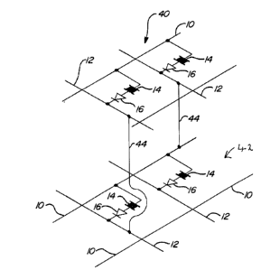
42. Figure lA depicts, in schematic form, a portion of a
stacked array of two matrices 40,42, each including unit
cells interconnected by a vertical via 44. Similar stacked
matrices are contemplated within the scope of the present
invention for the other unit cells shown herein.
Figure 2 depicts a unit cell including an excitory
18 input and inhibitory 20 input and a data output line 12.
This embodiment further includes a body of chalcogenide
material 14 and an isolation device 16 associated with each
of the input lines 18, 20. A unit cell of this type can
receive bipolar data which either stimulates or inhibits an
output response. In 'the foregoing unit cells, the body of
chalcogenide based material is set and reset by signals
applied to the data input lines 10, 18, 20 and the data
output lines 12.
Figure 3 depicts yet another embodiment of the
present invention which further includes a field effect
transistor 22 having 'the source and drain in series with a
data input line 10 and body of chalcogenide material 14.
The gate 24 of the transistor is energized by a separate
control line 26. 7.n a unit cell of this type, data
impressed on the control line 26 can further modify or
supplement data on t:he input line 10 so as to further
influence the setting and resetting of the chalcogenide
material 14.
16
CA 02052881 2000-11-24
Referring now to Figure 4 there is shown still
another embodiment of unit cell. This cell includes
excitory 18 and inhix>itory lines 20, each having a field
effect transistor 22 having the source and drain thereof in
series with a body of chalcogenide material 14 and an
isolation diode 16. The gates 24 of each of the transistors
22 are controlled by a common control line 28. In the
operation of a unit cell of this type, the common control
line 28 receives input: data, such as data from a pixel of an
image sensor and communicates this data to the unit cell.
Excitory and inhibitory data on the respective lines 18, 20
modifies the cell's response to this data so as to generate
an output which is communicated to other cells in the
processing net.
It is to be understood that the foregoing is
illustrative of particular unit cell configurations which
may be employed in the: present invention. Other variations
of unit cell may be similarly employed. The present
invention encompasses all parallel distributing processing
arrays having interconnected unit cells which include a body
of settable and resett:able chalcogenide based material. The
present invention readily lends itself to the fabrication of
neural net computing systems as well as various other
parallel processing devices.
17
CA 02052881 2000-11-24
Referring IlOW to Figure 5, there is shown an
exploded view schematically depicting one particular
configuration of neural network computer structured in
accord with the print:ipals of the present invention. The
. computing device of Figure 5 is an integrated computing
structure particularly adapted for image sensing and
processing. The computing device of Figure 5 includes a
sensor array layer 30 which comprises a matrix of
photosensitive elements arrayed in a pixel format. The
l0 matrix may be a two-dimensional array, i.e., an n x m array;
or, it may be a one-dimensional array, i.e., a 1 x n array.
The sensor elements may comprise photoresponsive devices
such as an amorphous silicon devices or other thin film
devices such as cadmium sulfide, cadmium telluride or copper
indium diselenide phot:oresponsive devices. The sensor array
30 is disposed to receive an image thereupon and to generate
parallel streams of data corresponding to the various pixels
of the image.
In most inst=ances, the computer includes a second
20 layer 32 of amplification circuitry comprised of a matrix of
amplifier devices corresponding in number to the
photoresponsive elemEants of the sensor array 30. The
amplification layer 3:? is operative to amplify the parallel
data streams generated by the sensor layer 30. Disposed in
electrical communication with the amplifier layer 32 is the
18
CA 02052881 2000-11-24
vertically interconnected parallel processing network 34
described herein above. The processing network 34 is
comprised of a number of stacked planes, each plane
comprising a matrix of unit cells corresponding generally to
the elements of the sensor array. The parallel data streams
from the sensor array are amplified and pass to the topmost
portion of the parallel processing network 34 and proceed
from the individual unit cells in the first plane to one or
more unit cells in the' second plane and thence onto further
l0 planes in the processing network 34. As was described
hereinabove, the strength of interconnections between cells
in superposed planes a re controlled via chalcogenide based
elements. The parallel distributing processing network 34
includes a number of ;stacked planes, each plane comprising
a matrix of unit cells. It is to be understood that the
number of unit cells i.n the various planes may be identical
or may vary. In some instances, it is desirable to have a
unit plane in a stacked relationship with a greater or
lesser number of unit cells in an adjoining plane and such
20 variations are contemg>lated within the scope of the present
invention.
The parallel processing network 34 is disposed
upon a silicon substrate 36, shown schematically herein as
a silicon wafer. The silicon substrate includes the drive
circuitry, multiplexing circuitry and interconnect circuitry
19
CA 02052881 2000-11-24
for establishing communication with the processing network
34. The substrate 36 can further include output contacts or
leads, not shown in this illustration. Silicon is a
preferred material for the substrate layer since the high
speed of crystalline silicon circuitry confers advantages in
the operation of the computing device; although it is to be
understood that other substrate layers, including layers of
semiconductor material having degrees of order ranging from
purely amorphous to polycrystalline may be similarly
employed.
While the Figure 5 embodiment depicts the sensor
array and amplification layers as being relatively thin
planes, it is to be understood that a representation herein
is schematic and the sensor array and amplification layer
may comprise multiple: stacked planes. It is also to be
understood that while sensor array has been described in
terms of a photosen:~or, other inputs may be similarly
provided. For example:, the sensor array 30 may be replaced
by a matrix of electrical inputs. Alternatively, various
other sensing devices. may be employed to input a signal
corresponding to acoustic, magnetic, thermal, pressure or
chemical inputs. For example, the sensor array 30 may be an
array of chemfets. These devices are field effect
transistors which respond to particular chemical species.
An array thus configured would be well adapted for sensing
CA 02052881 2000-11-24
chemical species and would have great utility and
characterization and classification of odors, detection of
bombs, gases or other noxious species as well as the
quantification of aromas such as perfumes, wines and
foodstuffs.
The chalcogenide based material is employed to
establish communication between the input and output means
of each unit cell and hence becomes a critical link in
establishing intracel:Lular communication. The chalcogenide
material may be set over a range of physical properties be
they optical, magnetic or electrical. For example, by an
appropriate input of energy the transparency and/or
reflectivity of the material may be reversibly set to a
plurality of values. Similarly, input of an appropriate
signal can change the capacitance, resistivity, or magnetic
permeability of these materials to different stable values.
In the most preferred embodiment of the present invention,
the computing system operates on electrical impulses and the
chalcogenide material is set and reset to a plurality of
values of electrical resistivity although it is to be
understood that in opi~ical computing systems, reflectivity
and/or optical transmission may be similarly employed.
Within the context of the present invention,
chalcogenide based materials are defined as being any
materials which include one or more chalcogenide elements
21
CA 02052881 2000-11-24
therein and it is generally understood that the chalcogenide
elements include the group VIa elements of the periodic
table. The chalcogenide based materials of the present
invention can also include elements such as carbon, silicon,
germanium, tin, lead, phosphorous, arsenic, antimony,
fluorine, oxygen or bismuth. One particularly preferred
group of chalcogenide materials are those referred to as
adaptive memory materials. These materials are reversibly
switchable from a highly disordered state to a more ordered
state and various degrees of local order or disorder
correspond to differE:nt values of resistivity or other
physical properties.
In a typical adaptive semi-conductor material, the
resistance may be altered from a value of about 106 ohms to
about 102 ohms by a current pulse of about 1 millisecond
duration having an amplitude of 5 milliamps or by an
equivalent pulse of light energy or the like. To obtain an
intermediate resistance value, intermediate values of
current are applied.
Referring now to Figure 6 there is shown a
schematic depiction of electrical properties of a typical
adaptive memory material. The Figure depicts a plot of the
log of the set energy applied to the material versus the log
of the electrical resi.stivity of the material. It will be
seen from the curve that the resistance decreases with
22
Oa/21/O1 08:59 FAX B13 239 3583 MacRae & Co. ~ 002
increasing set energy. It will also be seen that the
magnitude of the current flux applied to the material, even
~Inder equal energy c:onditi.dns, determines the final
resistance of the material_ It will thus be appreciated
that this material effectively provides a solid state
equivalent of a rheostat. By using an appropriate current
pulse, the resistance ~raJ-ue of the material may be set to
a stable value. By utilizing a material of this type in
the processor of the present invention, the degree of
connectivity between individual unit cells may be readily
set-
There are a number of compositions of
chalcogenide based adaptive memory material which may be
employed in the practice of the invention. The adaptive
memory materials qenera.lly contain Group IV and/or VI semi-
conductor materials and they further include Group V
materials such as phosphorous. When phosphorous ~.s
replaced by a high molecular weight Group v elements such
as arsenic, antimony, ete. the res~-stance versus energy
curve becomes, steeper. 1-adaptive memory materials are
detailed in U.S. Patent 3,53Q,441 of Ovshinsky. In view
of the foregoing it is to be understood that large area
parallel distributed. processing arrays may be
advantageousJ.y Constx'uCaed utilizing adaptive, settable and
resettable chascogenid~e
23
1i&21/U?/2001 ~ 8~5U X613 234 3563 received
V..~......_ . .. ~w.~._.,~,.._ ... ,. ~. ,._.. ._... _._..,w. _~~. ._.
CA 02052881 2001-02-21
CA 02052881 2000-11-24
materials. These arrays have significant utility in the
construction of neural network computing systems as well as
other data processing applications. The foregoing drawings,
discussion, description and examples are merely illustrative
of particular embodiments of the present invention. It is
to be understood that numerous modifications and variations
thereof may be practiced in accord with the principals of
the present invention. It is the following claims,
including all equivalents, which define the scope of the
invention.
24