Note: Descriptions are shown in the official language in which they were submitted.
~ ~ ~ 3 Q ~ ~
72430-156
REFLECTIVE OPTICAL MODULATOR
The invention relates to a reflective optical modulator.
Such modulators are employed in optical data trans-
mission systems in which a line end device generates the signal
to be transmitted without having an available light source. The
optical carrier for such a transmission signal in these systems
is generated in a central station and is conducted to the line
end device by way of an optical waveguide, is modulated there,
and the resulting transmission signal is transmitted preferably
over the same optical waveguide.
The publication entitled, Electronics Letters, May 8,
1986, Volume 22, No. 10, pages 517 and 518, discloses such a
system which includes a reflective modulator. The disclosed
reflective modulator is composed of an electro-optically active
waveguide coupler which can be operated as a switch and is
included in an integrated optical circuit.
It has two branches each having two terminals. The
optical waveguide for the transmission of data is disposed at a
first terminal of the first branch and the reflective surface is
disposed at a first terminal of the second branch. By way of
suitable switching, light entering the modulator from the optical
waveguide can be reflected back from the reflective surface into
the optical waveguide. If one considers the light entering into
the modulator as an optical carrier and the switching as
modulation, it can be said that an optical transmission signal is
generated by modulation of the carrier.
The drawback of the prior art reflective optical
modulator is now that the adjustment between the optical waveguide
~;A
72430-156
and the integrated optical circuit in which the reflective
modulator is disposed must be very accurate and is therefore
correspondingly expensive from a technology aspect.
It is now an object of the invention to create a
reflective optical waveguide in which this drawback does not
occur.
According to a broad aspect of the invention there is
provided a reflective modulator including: an optical waveguide;
a reflecting surface arranged opposite an end face of the optical
waveguide; and modulation means for modulating, with a modulation
signal, light exiting from the end face of the optical waveguide
and coupled back into the optical waveguide by the reflecting
surface; wherein the modulation means comprises a detunable
optical resonator having first and second reflective surfaces
disposed opposite one another, the first reflective surface of the
resonator being said reflecting surface and the second reflective
surface of the resonator being the end face of the optical
waveguide; wherein the modulation signal controls detuning of the
optical resonator to thereby effect modulation of the light; and
wherein at least one of the first and second reflective surfaces
is tiltable with respect to the other reflective surface under
control of the modulation signal.
According to another broad aspect of the invention there
is provided an optical transceiver module including a reflective
modulator comprising: an optical waveguide; a reflecting surface
arranged opposite an end face of the optical waveguide; and
modulation means for modulating, with a modulation signal, light
72430-156
exiting from the end face of the optical waveguide and coupled
back into the optical waveguide by the reflecting surface; wherein
the modulation means comprises a detunable optical resonator
having first and second reflective surfaces disposed opposite one
another, the first reflective surface of the resonator being said
reflecting surface and the second reflective surface of the
resonator being the end face of the optical waveguide; wherein the
modulation signal controls detuning of the optical resonator to
thereby effect modulation of the light; wherein light passing
through the first reflective surface can be detected as a received
signal in a photodiode disposed behind the first reflective
surfa~e; and wherein the first reflective surface is a surface of
the photodiode through which light enters the photodiode to be
detected.
Further features of the invention are disclosed in the
remainder of the specification.
A particular advantage of the invention is the use of
the reflective modulator according to the invention in a
transceiver module. It is advantageous that no coupler is
required to divide the carrier power into a part for the
photodiode and a part for the reflective surface and that, when
operated as a transmitting module, no interfering reflections from
the surface of the photodiode are mixed into the transmitted
signal in the transceiver module.
2a
20S3022
Another advantage of the invention lies in that the
required components are obtainable on the market as mass
produced items.
Five embodiments of the invention will now be described
with reference to seven drawing figures. It is shown in:
Fig. 1, the basic principle of the reflective optical
modulator according to the invention;
Fig. 2, the relative level of the power reflected back
into the fiber plotted over the resonator
length x;
Fig. 3, a first embodiment of a reflective optical
modulator including a compression-type
resonator as the vibratory element;
Fig. 4, a second embodiment of a reflective optical
modulator including an electro-optically
active medium to vary the resonator length x;
Fig. 5, a third embodiment of a reflective optical
modulator including a flexural resonator as
the vibratory element;
Fig. 6, an embodiment of a transceiver module; and
Fig. 7, an embodiment of an optical transmission
system.
20~3022
,~".
Figure 1 shows the basic principle of the reflective
optical modulator according to the invention. For the sake
of simplicity, the reflective optical modulator will herein-
after be simply called modulator. Modulator 1 includes the
following components: one end face of an optical waveguide 2
through which light exits. This end face will hereinafter be
called the second reflective surface 4. It lies opposite a
first reflective surface 3. Reflective surfaces 3 and 4 lie
parallel to one another and thus form a Fabry-Perot reson-
ator 5 which has a resonator length x between the two reflec-
tive surfaces 3 and 4. The resonator length x is an optical
length, i.e. the refractive index of a medium contained in
the Fabry-Perot resonator 5 has been considered.
Light of a power level PT is coupled into the Fabry-
Perot resonator 5 through the second reflective surface 4 and
is at least partially reflected at the first reflective
surface 3. Thus some of the light is coupled back into the
optical waveguide 2 by way of the second reflective surface
4. This causes a standing wave to be formed in Fabry-Perot
resonator 5. The typical course of the portion of the light
at power level PR reflected into optical waveguide 2 with
reference to the power level PT of the incident light is
plotted in Figure 2 over the resonator length x. It can be
seen that the relative power level PR/PT fluctuates
-- 4
2053022
periodically between a minimum power level Pl which is less
than -40 dB and a maximum power level P2 around -8 dB. The
period distance xO is equal to half a wavelength of the light
which, for a wavelength of, e.g. ~o = 1300 nm, corresponds to
a value of xO = 650 nm. By varying resonator length x it is
thus possible to change the power level PR of the light
component reflected back into optical waveguide 2 and thus it
is possible to amplitude modulate the optical carrier. This
variation will hereinafter be called the modulation devia-
tion.
The variation in resonator length x here constitutes
only a special type of detuning of Fabry-Perot resonator 5.
Resonator 5 may also be detuned by tilting one of the two
reflective surfaces 3, 4 out of its plane or by deforming one
of the two reflective surfaces 3, 4, or in some other way or
by a combination of the above mentioned possibilities. The
realization of a modulator by utilizing some of the mentioned
detuning possibilities will be demonstrated below in the
embodiments.
In order to reduce divergence losses in the light energy
when the light exits from optical waveguide 2, resonator 5
may include an optical imaging system in the beam path
between the two reflective surfaces 3 and 4.
2053 G22
Due to the divergence of the light exiting from the
optical waveguide 2, it is not absolutely necessary to employ
a Fabry-Perot resonator 5 having two parallel reflective
surfaces 3 and 4 as the resonator. If the normals on the two
reflective surfaces 3 and 4 enclose an angle other than zero
degrees, the first reflective surface 3 reflects diffracted
exiting light from optical waveguide 2 back into optical
waveguide 2. If the angle enclosed by the normals on the two
reflective surfaces 3 and 4 is selected to be other than zero
in the quiescent position, it is recommended to select the
degree of reflection of the first reflective surface 3 to
decrease with increasing angle.
Advantageously a glass fiber lightguide is employed as
optical waveguide 2. The second reflective surface 4 is then
an end face of the glass fiber lightguide and is preferably
disposed at a right angle to the glass fiber sheath.
The quality of resonator 5 can be adjusted in that the
degree of reflection of reflective surfaces 3, 4 is changed
in a known manner, for example, in that selected layers are
applied.
Figure 3 shows a first embodiment in the form of a
modulator 20. In addition to the above-described features
shown in Figure 1, modulator 20 includes as a mechanical
vibrator device a compression-type resonator 8 in the form of
2053~22
a piezoelectric transducer having electrical terminals 7 to
which can be applied a modulation voltage Umr that is, the
modulation signal. The first reflective surface 3 is
connected with piezoelectric transducer 8 in such a way that
the resonator length x is changed by the application of
modulation voltage Um.
Figure 4 shows a second embodiment in the form of a
modulator 30 in which detuning is also effected by varying
the resonator length x. For this purpose, a birefringent
medium 9 is disposed between two electrodes E to which the
modulation voltage Um is applied. The refractive index x of
medium g can be varied by the application of modulation
voltage Um. A change in the refractive index of medium 9
changes the resonator length x. The first reflective surface
3 lies on a surface of medium 9 that lies at a right angle
to the faces against which electrodes E lie. The second
reflective surface 4 is located on the side of medium 9
opposite the first reflective surface 3.
The third embodiment in the form of a modulator 10 is
shown in Figure 5. Compared to modulator 20 of Figure 3, the
compression-type resonator 8 of this modulator 10 has been
replaced by a flexural~resonator 6, preferably a quartz
oscillator. The Fabry-Perot resonator 5 of this modulator
10 is detuned by a combination of varying the resonator
' 2053022
length x and tilting the first reflective surface 3 out of
its quiescent plane.
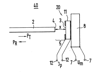
Figure 6 shows a transceiver module 40 which is equipped
with a modulator according to the invention, here modulator
20 of the second embodiment. In order to receive data
signals, a photodiode 11, for example a PIN photodiode, is
disposed on compression-type resonator 8. The first reflec-
tive surface 3 here constitutes the entrance surface for the
light into photodiode 11. The generated photocurrent Ip
flows through terminals 12.
Photodiode 11 detects the light that enters at power PT
minus the reflected component. Since the generated photocur-
rent Ip is only slightly dependent upon the resonator length
x, there is no interfering modulation of photocurrent Ip due
to the variation of resonator length x. A typical value for
the interference lies below 1 dB.
A particular advantage of the modulator 10, 20, 30
according to the present invention compared to the prior art
modulator is the uncomplicated coupling between optical
waveguide 2 and Fabry-Perot resonator 5. Modulators 10, 20,
30 require merely a coupling of the quality of an average
waveguide-photodiode coupling, whereas the prior art modulat-
or, due to its "integrated optical waveguides", requires a
coupling of the higher quality of a waveguide-laser coupling.
20~3~22
.,~
The arrangement of a flexural resonator 6 in a trans-
ceiver module 40 reduces the coupling problem compared to the
prior art transceiver module at least in the adjustment
direction which lies in the direction of movement of flexural
resonator 6.
The complete operation of the transceiver module will
now be described in connection with the embodiment of an
optical data transmission system ON. The data transmission
system ON includes a central station Z and several sub-
scribers Ti, where i = 1, 2, ..., N. As an example, only the
transmission from central station Z to a subscriber Tl and
back will be described here. Central station Z includes a
laser module S which generates a carrier of a wavelength ~o =
1300 nm modulated with a frequency fo = 5 MHz. This modu-
lated carrier is transmitted by way of a star distributor S
and an optical waveguide AL to a transceiver module SE at
subscriber end Tl and is received there. In transceiver
module SE, the light is modulated by the reflective optical
modulator with a modulation frequency fl = 600 kHz. Care
must be taken that the modulation bands, including the
sidebands and the harmonics, are not superposed on one
another. The reflected signal modulàted with frequency fl is
now transmitted over the same optical waveguide AL and star
distributor S to central station Z and is there fed by way of
2053G22
.~,
a 3dB power coupler K to an optical receiver module E. The
latter is followed by an electrical receiver which filters
out the desired band, for example at the modulation frequen-
cy fl, and demodulates it.
If the modulation in transceiver module SE is effected
by means of a vibration of the first reflective surface 3
over several oscillation nodes of the standing wave in Fabry-
Perot resonator 5, non-linearities also produce interfering
modulations in each case at a band spacing of modulation
frequency fl = 600 kHz. These interfering modulations can be
filtered out electrically in receiving module E in the above
described manner.
In order to transmit from transceiver module SE of
carrier 1 El to central station Z in the baseband, it is
necessary to limit the modulation deviation in the reflective
optical modulator to a value of about ~0/4. The operating
point preferably is removed from one of the oscillation
antinodes of the standing wave by ~o/8.
The transmission from central station Z to the sub-
scribers and in the opposite direction is effected by way of
signals that are coded with an NRZ (non-return to zero) code.
These signals may be amplitude, phase or frequency modulated.
The optical data transmission system ON makes it
possible to supply several subscribers Tl by means of a
-- 10 --
2~53022
single laser module S disposed in central station Z and by
way of star distributor S. The subscribers, in turn, are
able to transmit signals directed to central station Z by
modulating the received carrier. The identification of the
individual subscriber signals in central station Z is made by
the use of different frequency fl for the subcarrier.
In this embodiment, the transmission in the downward
direction is broadbanded, for example, for cable television
and telephone; the transmission in the upward direction is
narrowbanded, for example, only for telephone. However,
particularly if a modulator 30 according to the second
embodiment is employed, a symmetrical broadband transmission
is also possible.
-- 11 -- - .