Note: Descriptions are shown in the official language in which they were submitted.
PROGRAP2MABLE CONTROLLER PROCESSOR WITR
AN IUTELLIGENT FU~CTIO~AL MODULE INTERFACE
The present invention relates to programmable controllers
for operating industrial equipment, and more specifically to
the processors in such programmable controllers which interface
to a series of functional modules via a set of buses.
Programmable controllers are a common type of industrial
computer for operating a variety of manufacturing equipment,
such as assembly Lines and machine tools, in accordance with a
stored control program. The program comprises a series of
process control instructions which are read out and executed
to examine the condition of selected sensing devices on the
controlled equipment, and to energize or deenergize selected
operating devices contingent upon the status of one or more of
the examined sensing devices.
The state of many sensing and operating devices can be
represented by a single bit of data which is manipulated by the
control program instructions. Other devices, such as position
sensors, provide multiple bits of data representing a condition
of the equipment being controlled. Far these latter devices,
instructions are provided to manipulate bytes and words of data
representing the state of the sensing and operating devices.
Additional program instructions perform arithmetic operations,
timing and counting functions, and complex statistical
reporting operations. Such instructions have become quite
standardized in the industry and are directly associated with
the elements of a ladder logic diagram which is easily
understood~by process control engineers. Program panels such
as those described in U.S. Patent Nos. 3,808,612; 3,813,649 and
_1_
20~~126
4,070,702 have been developed to assist the user in developing
and editing ladder logic control programs comprised of such
programmable controller instructions.
The Allen-Bradley 1771 series programmable controllers
are an example of this type of industrial computer. A 1771
programmable controller includes a rack having a number of
slots which hold different kinds of functional modules. One
slot holds a processor module that stores and executes the
user-defined control program. The control program is executed
repeatedly thereby performing the same logical operations over
and over again for different workpieces being processed by the
controlled equipment. Input and output modules, which
electrically interface to sensing and operating devices on the
controlled equipment, are positioned in other rack slots. The
rack has an backplane with conductors 'to which the modules
electrically couple, thereby enabling 'the exchange of data and
control signals. For example, the processor module gathers
data from the input modules representing the status of the
sensing devices, and issues control commands to the output
modules to which the operating devices are connected. The
data is gathered and the commands are issued by the processor
module over the rack backplane.
Many applications of programmable controllers require
relatively high speed processing of input and output data.
One example of such processing involves counting inputs for
tracking the production of items, such as counting containers
passing along a food canning line. In another example, a need
may exist to respond immediately to a given input signal by
taking the appropriate action, such as quickly clamping a
workpiece when its presence is detected. These events may
occur more frequently than once every execution cycle through
-2-
~o~~~~~
a ladder logic program, occurring while another task is being
performed. Therefore, its is desirable to provide a processor
module with the capability to monitor selected inputs and
perform simple logical operations without requiring processing
time of a microprocessor in the module.
A programmable controller includes a processor module and
a plurality of input and output (I/O) modules housed in a rack
and electrically connected together by a backplane of the
rack. The input and output modules interface to sensing and
operating devices on machinery operated by the programmable
controller. The processor module executes a user defined
control program which examines the status of selected sensing
devices and sets the states of specified operating devices in
accordance with the examined status.
The unique processor module includes a microprocessor,
memory and an I/0 interface circuit coupled together by a
common set of internal signal buses. The T/0 interface circuit
controls the exchange of data over the rack backplane with the
I/0 modules. This circuit performs conventional transfer
functions for exchanging both single bytes and multiple byte
blocks of data with the I/O modules. In addition, the I/0
interface circuit is programmable to pre-process input data
before it reaches the microprocessor. A predefined input
transition can be detected and in response, either interrupt the
microprocessor or count the transition, interrupting the
microprocessor only after a given number of transitions occur.
Upon being interrupted the microprocessor executes a correspond--
-3-
2~53~.~~
ing interrupt routine which~responds to the detected input
condition.
A general object of the present invention is to provide a
programmable controller processor module with an intelligent
interface circuit to handle the exchange of data with I/0
modules. Such an interface circuit frees the program execution
processor from handling I/0 module data transfer.
Another object of the present invention is to provide a
programmable controller processor module in which the occurrence
of defined input transitions can be detected without the
intervention of the microprocessor.
A further object is to provide the interface circuit with
the capability to preprocess incoming data according to
configuration data specified by a user.
Bri~f es~~~i~~ic~n o~ tha Dry
FIGURE 1 is a perspective view of a programmable controller
system employing the present invention;
FIGURE 2 is a functional block diagram of a processor
module which forms part of the controller of Figure 1;
FIGURE 3 illustrates the data structures of the shared
system memory in the processor module;
FIGURE 4 is a block diagram of the I/0 interface circuit
in the process or module;
FIGURE 5 depicts a block of storage locations in a shared
memory of the processor module to store configuration data for
a programmable input interrupt function;
FIGURE 6 is a flow chart of one portion of the
programmable input interrupt function;
-4-
~0~312~
FIGURE 7 is a schematic representation of the equivalent
hardware for performing the function depicted by the flowchart
of Figure 6;
FIGURE 8 is a flowchart of another portion of the
programmable input interrupt function; and
FIGURE 9 is a data block containing the results of the
programmable input interrupt function.
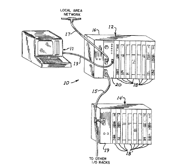
Referring to Figure l, a programmable controller system
generally designated as 10 comprises a primary equipment rack
12 arid a series of remote input/output (I/0) racks, such as
rack 14, interconnected by a serial I/0 network 15.
The primary rack 12 houses a power supply, processor
module 20 located in the first, and a plurality of input/output
interface modules 18 housed in other slots. The processor
module 20 executes a user-defined control program that responds
to signals from sensing devices on thE: controlled equipment
(not shown) by issuing signals to actuating devices on the same
equipment. The sensing and actuating signals are coupled to
the rack 12 through the input/output interface modules 18.
The various modules 18 and 20 within the primary rack 12 are
electrically interconnected by conductors on a backplane 16 of
the rack enabling data, address and control signals to be
exchanged among the modules.
The processor module 20 receives program instructions via
a terminal 11 that is connected by cable l3 to a serial port
connector on the front panel of the module. The T/0 network
15 is coupled to another connector on the front panel of the
processor module 20 and to an adaptor module 19 in the remote
I/0 rack 14, enabling the processor module 20 to exchange data
_5_
20~3~26
with another group of I/0 modules 18° within the remote I/0
rack. A local area network (LAN) 17 is coupled to a third port
connector on the front panel of the processor module 20 enabling
the module to communicate with a host computer and other
programmable controllers coupled to that network. For example,
communication via LAN 17 enables a host computer to direct the
operation of a plurality of programmable controllers such as
device 10 in order to supervise a complex manufacturing system.
Whereas previous programmable controllers utilized
ZO separate modules within the primary rack 12 to perform the
program execution, host communication and remote I/0 rack
communication functions, the present system incorporates all
of these functions within the 'processor module 20. By doing
so, the communication between the modules 18 in rack 12 via
the rack backplane has been reduced to exchanging data
representing the state of the sensing and actuating devices on
the control equipment.
Referring to Figure 2, the processor module 20 includes a
general purpose processor section 60 for user control program
execution and two communication processor sect9.ons 21 and 70 to
handle the exchange of data over cable 13 and networks 15 and
17. As will be described in detail, each of these sections of
the processor module has its own microprocessor and local memory
coupled by an isolatable set of address, data and control buses.
The processor module 20 also has a set of shared buses 33-35
which connect these sections 21, 60 and 70 together and to other
data processing and storage components.
A first communication processor section 21 is formed
around a local address bus 23 and a local data :us 24. Coupled
to these buses is a first microprocessor 22 which executes a
program stored in a first read only memory (ROM) 26 and
-6-
2~53i~~
utilizes a first local random access memory (RAM) 27 as a
scratch-pad for temporary data storage. A master clock circuit
30 provides a system clock signal for other components within
the processor module 20 as well as providing specific timing
signals via control lines 25 to the components of the first
communication processor section 21.
The primary function assigned to the first microprocessor
22 in the exemplary processor module is the control of
communication with the programming terminal 11 and the hAN 17.
A UART 23 couples the local address and data buses 23 and 24 to
the terminal via cable 13. The DART 28 is anv of several
commercially available devices which interface the parallel
data format within the processor module 20 to a serial
communication format for communicating with the terminal 11.
Although the module port from the UART 28 is illustrated as
connected to the programming terminal 11, this port can be
coupled to other types of serial devices for the exchange of
data with the processor module 20. The local address and data
buses 23 and 24 are coupled to a first network interface 29 so
that the first microprocessor 22 can exchange data over LA.N 17
with other devices. The first network interface converts the
parallel data within the processor module 20 into a serial
formatted message packet which is compatible with the protocol
employed to communicate with the devices on hAN 17.
The first communication processor section 21 is connected
to other processor module sections through a set of tri-state
address gates 31 and a set of bi-directional tri-state data
gates 32. Specifically, the set of gates 31 couples the local
address bus 23 to the module's shared address bus 33, and the
set of data gates 32 couples the local data bus 24 to a shared
data bus 34. A set of control lines 35 extend between processor
_7_
20~~26
module components and hereinafter is referred to as a control
bus.
This coupling of buses allosas the first microprocessor 22
to write and read data t o and from a shared system RAM 36
coupled to the shared address and data buses 33 and 34. The
organization of data within the shared system RAM 36 is
illustrated in Figure 3. A block of shared system RAM storage
locations contains a conventional set of data tables 41-43 for
the processor module 20. The first of these data tables 41
stores input data representing the state of the sensing
devices coupled to the controlled equipment. Data from input
type I/0 modules 18 in the primary and remote racks 12 and 14
are stored in an organized manner in this table 41. A second
data table 42 stores output data representing the state of the
actuating devices on the equipment which are operated by the
programmable controller system 10. Using a similar
organization, the output table 42. stores the data employed to
control the actuating devices connected to output type I/0
modules 18 in racks 12 and 14. Another data table 43 contains
information regarding the status of the programmable
controller 20 and its components. As may be necessary,
additional data tables can be stored in the shared system RAM
36.
A block of storage locations 44 in the shared system RAM 36
stores the user-defined control program. Depending upon the
specific definition of this program given by the user, this
block 44 may store a single ladder logic control program or a
series of such programs to be executed in a sequence defined by
a conventional function chart. Tn the latter case, the function
chart data files also are stored in memory block 44 along' with
the ladder logic control programs. Following the storage
_g_
~o~~~2s
locations used by the control program is a section of free
memory locations 45. Another section of the shared system RAM
contains an I/0 force data table, similar to that used in
previous programmable controllers to force the control data from
specific sensing or actuating devices to a given logic state. A
section 47 of storage locations at the high addresses of the
shared system RAM 36 is used to contain system, processor
module, and microprocessor level configuration data. For
example, the configuration data defines password and privilege
information, port communication parameters and event timeout
intervals.
Referring again to Figure 2, a ladder logic processor 50
is also coupled to the shared address and data buses 33 and 34.
The vast majority of ladder control program instructions
operate on a single bit or word of data. The ladder logic
processor 50 has been designed t o execute the subset of ladder
diagram instructions which perform these basic control
operations. This not only provides efficient execution of
frequently occurring instructions, it also frees the
microprocessors in the module 20 to carry out other functions
simultaneously with the control program execution. The ladder
logic processor 50 also arbitrates among competing requests
from processor module components for access to the shared buses
33-35 and grants such access based upon a predefined priority.
Certain functions, such as data block transfers to the I/0
modules 18 and complex mathematical and logical operations
cannot be performed by the ladder logic processor 50. These
complex control program functions are executed by the general
purpose processor section 60. This section of the processor
module 10 contains a second microprocessor 61 connected to its
own isolated set of address and data buses 62 and 63,
- 9-
respectively. This pair of buses 62 and 63 couples the second
microprocessor 61 to a second ROM 64 and a second local random
access memory 65. The second ROM 64 stores the firmware which
.is executed by the second microprocessor 61 to carry out the
more complex ladder logic operations. The firmware in ROM 64
also interprets the function chart when one is defined by the
user.
Many of the user control program instructions which the
ladder~logic processor 50 cannot perform are complex arithmetic
operations. Therefore, a conventional math co-processor 66 is
provided to execute the corresponding instructions more
efficiently than by using the second microprocessor 61. A
timing circuit 67 receives the system clock signal and derives
therefrom the necessary timing and control signals for the
second micropracessor 61, memories 64 and 65, and the math
co-processor 66. A pair of tri-state transmission gates 68 and
69 isolate address and data buses 62 and 63, respectively of the
general purpose processor section 60 from the shared address and
data buses 33 and 34. When these gates 68 and 69 are enabled in
response to a command from the second microprocessor 61, the
internal set of buses 62 and 63 are electrically connected to
shared buses 33 and 34. This enabling occurs only when the
second microprocessor 61 requires access to the shared system
memory and has been granted access to buses 33 and 34 by an
arbitration circuit in the ladder logic processor 50.
As described above, the processor module 20 is coupled
via I/0 network 15 to one or more remote I/0 racks 14. The
processor module utilizes a second communication processor
section 70 with a third microprocessor 71 to control the
gathering of sensor data and the transmission of actuating
device state commands to these remote racks. The third
-10-
microprocessor 71 is coupled to another set o.f isolated address
and data buses 72 and 73 and a set of control lines 78. A
third ROM 74 is connected to these buses and stores the
firmware which is executed by the t';.ird microprocessor 71 to
perform its communication function. A third level RAM 75
provides a scratch-pad memory and temporary storage location
for the data being communicated over cable 15.
A second network interface 76 translates the para1121
data format within the processor module into the serial format
and the specific protocol used to communicate the data over the
I/0 network 15. A timing circuit 77 receives the system clock
signal from the master clock circuit 30 to provide the
necessary timing signals for the components associated with the
third microprocessor 71. These timing signals are transmitted
via some of the control lines in set 78.
The address bus 72 coupled to the third microprocessor 71
is connected to the shared address bus 33 by a set ~f tri-state
gates 78. Similarly, the data bus 73 associated with the 'third
microprocessor 71 is coupled to the shared data bus 39 by a set
of tri-state, bi-directional gates 80. Both sets of gates 71
and 80 are enabled by signals via control lines 78 from the
third microprocessor 71. The gates are enabled when the third
microprocessor 71 has been granted access to the shared buses
33 and 34 by the arbitration circuit within the ladder logic
processor 50.
Referring still to Figure 2, an I/0 rack interface circuit
38 is connected to the shared address and data buses 33 and 34
and the backplane 16 of primary rack 12. This interface circuit
periodically scans the I/0 modules 18 in the primary rack to
gather input data from the sensors on the controlled machinery
and send output data to the actuating devices. This
-11-
205326
conventional scanning is accomplished in a manner similar to
that employed by previous processor modules by sequentially
sending control signals to each I/0 module. These control
signals cause input type modules to send sensor data over the
backplane 16 and cause output type modules to store data sent by
the processor module. The data exchanged with the I/0 modules
18 in the primary rack 12 can be stored in the I/0 data tables
41 and 42 of the shared system RAM 36.
The details of the I/0 rack interface circuit 38 are shown
in Figure 9. The I/0 rack interface circuit 38 comprises a
circuit controller 100, backplane controller 102, an
arbiter/sequencer 104 and timer circuits 106. The circuit
controller 100 interfaces the I/0 rack interface circuit 38 to
the shared buses 33-35 of the processor module 20 and provides
general supervisory control of the interface circuit operation.
To this end, the shared address bus 33 is coupled by a first set
of bi-directional data gates 108 to a supervisory processor 110.
Similarly, the shared data bus 34 is coupled by a second set of
bi-directional data gates 109 to the supervisory processor 110.
The control lines of the processor module 20 are connected
directly to the supervisory processor.
The supervisory processor 110 executes a micro-code program
stored within a first micro-code ROM 112 and stores the results
of the processing and data being exchanged over the backplane 16
in a first interface RAM 114. The operation of the supervisory
processor 110 will be described subsequently in the course of a
description of the operation of the entire I/0 rack interface
circuit 38.
The circuit controller 100 also contains an interrupt
encoder 116 which receives signals from the arbiter/sequencer
104 and the timer circuits 106 indicating the occurrence of
-12-
various processing events, as will be described. In response to
these input signals, the interrupt encoder 116 generates
interrupt signals on lines 117 and 118 which respectively
interrupt .the supervisory processor 110 or other components of
the processor module 20 via the set of control lines 35.
The supervisory processor also has a set of control lines
119 and an I/0 request bus 120 which are connected to the
arbiter/sequencer 104 to control the operation of that latter
component. A set of data bus lines 121 extend between the
supervisory processor 110 and a backplane processor 122 in the
backplane controller section 102. The arbiter/sequencer 104 is
also coupled to the backplane processor 122 by address lines 129
and a set of control lines 125.
The timer circuit 106 is coupled by several lines to the
arbiter/sequencer 104, the supervisory processor 110 and the
interrupt encoder 116. The backplane processor 122 also
produces control signals which are coL~pled to the timer circuit
106.
The backplane controller section 102 consists of not only
the backplane processor 122, but also a second micro-code ROM
126 which stores a micro-code program for execution by the
backplane processor. A second interface RAM 128 is contained
within the backplane controller for storing processing results
and data for the backplane processor 122. Additional ports of
the backplane processor 122 are connected to a set of control
lines and a data bus 131 of the backplane 16 in rack~l2. As
will be described, the backplane controller section 102
generates control signals to regulate the transfer of data
between the processor module 20 and the backplane 16 and can
perform rudimentary processing of the input data received from
functional modules 18.
-13-
2n~~~26
The T/0 rack interface circuit 38 supervises the exchange
of data across the backplane of rack 12. This includes standard
discrete (one word) and data block (multiple word) transfers and
several priority levels of each type of transfer. The technique
by which blocks of data are transferred is described in U.S.
Patent No. 4,293,924. The I/O rack interface circuit handles
the following types of I/Q requests from other processor module
components in the following descending priority order:
Block Transfer Timeout
Pragrammable Input Interrupt (PII)
Priority immediate I/0
Priority Block Transfer
Discrete I/0 Scan
Normal Immediate I/0
Normal Block Transfer
The first type of I/0 request occurs upon the expiration of
internal timers in circuit 106 that were set by the user control
program. The programmable input interrupt (PII) will be
described in detail subsequently. The discrete I/0 scan is a
conventional exchange of data between all of the modules in the
primary rack 12 and the I/0 image tables in blocks 41 and 42 of
the shared system RAN1 36. This exchange typically occurs just
prior to each execution pass through the user-defined control
program. The priority and normal immediate I/0 requests are
similar to well-known processes in which a single word of data
is transferred over the backplane in response to an instruction
in the user defined control program.
Depending upon the number of inputs or outputs in the
module to or from which the data is to be transferred, each
type of I/0 request mad require the rack interface circuit 38
to perform several backplane signal cycles. For example, each
. slot of rack 12 may contain a single density module with only
eight I/0 points or a double density module with sixteen I/0
points. Quad and octal density modules can be used which
-14-
~o~~~~~
provide 32 and 64 I/0 points respectively. Since data is
transferred over the rack backplane in byte sized amounts,
multiple transfers are required for higher density modules.
Transfer techniques for higher density modules are described
in U.S. Patent No. 4,691,296. For data exchange purposes, the
rack slots are grouped in pairs, with one slot of the pair
designated as a high slot and the other as a low slot, and
both slots being collectively referred to as a "group".
Thus, the seven I/0 requests listed above are carried out
by selected ones of eighteen different backplane signal-cycles
by the rack interface circuit 38. These cycles are:
null
I/0 read low slot
I/0 read high slot
I/0 write low slot
I/0 write high slot
block transfer write Module Control Byte
block transfer read Module Status Byte
block transfer read low slot
block transfer read high slot
block transfer write :Low slot
block 'transfer write high slot
block transfer read checksum
block transfer write checksum
PII read low slot
PII read high slot
wait
load diagnostic
read diagnostic
A null cycle is executed when a backplane signal cycle is not
requested and a wait cycle is executed if the previous cycle has
not completed. Control data is sent to a module via the block
transfer write module control byte cycle and its status obtained
with the block transfer read module status byte. The two
diagnostic cycles are used at power-up to test the backplane
controller 38. The PII cycles will be described subsequently
-15-
~0~~~2~
and the functions of 'the remaining cycles are obvious from their
names.
The operation of the I/0 rack interface circuit 38 may be
better understood through a description of how a discrete data
transfer occurs at power-up after diagnostic routines are run.
During system initialization, the general purpose processor 60
loads configuration data into the section of data block 47 of
share RAM 36 that is assigned to the I/0 rack interface circuit.
One group of this data identifies the type and size of the
primary rack 12 and the density of the module in each rack slot.
This configuration data is used by the circuit 38 in determining
how to send and receive data over the backplane 16.
When the general purpose processor 60 desires to send or
receive data to or from a module in the primary .rack 12, it
sends the appropriate request to the I/0 rack interface circuit
38. This I/0 request specifies 'the 'type of module access
(discrete, block transfer, priority level, etc.) and the slot iri
which the module is located. The I/0 :request is sent over the
snared buses 33--35 in the processor module 20. The I/0 rack
interface circuit 38 recognizes 'that control signals on bus 35
indicate that a primary rack I/O request is being sent, and the
circuit controller 100 receives and stores the command.
Upon receipt of the I/0 request, the supervisory processor
110 in the circuit controller 100 of Figure 4 begins executing a
firmware routine that is read from the first micro-code ROM 112
to process the command. At this point, the circuit controller's
function is to translate the I/0 request into a format that the
arbiter/sequencer 109 can manipulate. The formatted I/0 request
is sent by the supervisory processor 110 to the arbiter/
sequences 109 via the I/0 request bus 120 along with control
signals on line 119. Upon receipt, the I/0 request is stored in
-16-
a request register in the arbiter/sequencer along with other I/0
requests awaiting handling.
When the the backplane controller 102 is available,
arbiter/sequencer 104 scans the request register for the I/0
request with the highest priority. If several I/0 requests at
the same priority exist, they will be handled in rack slot order
going away from the processor module 20 in a rotating round
robin arbitration scheme. The arbiter/sequencer 104 is
essentially a state machine which takes the I/0 request of the
highest priority and sends the proper control signals to the
backplane controller 102. For example, if the I/0 request is to
perform an immediate input from a given module in the low slot
of a group, the arbiter/sequencer 104 will request the backplane
controller to execute a number I/0 read low slot cycles
depending upon the density of the module, i.e. how many bytes of
input data it provides. The density of the module is indicated
by configuration data stored in the section 47 of the shared
system RAM 36.
When the backplane controller 102 receives a backplane
signal cycle execution request from the arbiter/sequencer 104,
the backplane processor 122 decodes the cycle designation to
address the routine in second micro-code ROM 126 that performs
that backplane cycle. In the course of executing this micro-
code routine, the backplane processor 122 responds to the
instructions by applying the properly timed sequence of
control signals to the backplane 16 of the primary rack 12.
If the requested I/0 function is a block transfer type, the
word of data being exchanged, a checksum and a module control
byte will be stored temporarily in the RAM 128 of the
backplane controller 102. Otherwise, the bytes of data being
exchanged is transferred directly between the functional
-17-
2~~3~26
module and a register in the circuit controller 100 via data
bus 121. If the I/0 request is an input type, once the data
has been stored in the interface circuit 38, the supervisory
processor 110 requests access to the shared buses 33-35 of the
processor module 20. Once that bus access has been granted
th4 supervisory processor 110 transfers the data either to the
shared system RAM 36 or the requesting processor section 21,
60 or 70 depending upon the type of request.
One of the unique features of the I/0 rack interface
circuit 38 is the ability to perform rudimentary pre-processing
on defined input signals from the rack modules without
intervention by a processor section. This function is referred
to herein as a programmable input interrupt (PII). The PII
feature enables the user to define a pattern of one or more
input bit level transitions for the interface circuit 38 to
detect. Further, the circuit can be programmed to interrupt the
second microprocessor 61 either after every occurrence of the
designated transition pattern or only after a given number of
such transitions has occurred.
The PII function is enabled and configured by data that is
stored in section 47 of the shared system RAM 36. A flag bit in
the general configuration data for the I/0 rack interface
circuit 38 is set to enable the PII function. If this function
is enabled, the general configuration data also contains a
pointer to a configuration data block 140 for the PII function.
This data block 140 is depicted in Figure 5 and consists of .five
data words. The first word 141 is a mask which is to be ANDed
with input data word to select the bits to be tested for a
transition. Each bit of this mask is set to a high logic level
if the corresponding bit of the input data word is to be tested
for a transition. The second PII configuration word 142 is a
-18-
2~~3~~6
polarity mask in which specifies the direction of the transition
to be detected. In this polarity mask, a high bit designates
that a low to high transition of the corresponding input bit is
to be detected, whereas a low bit designates the desired
detection of a high to low transition. The third word 143 of
the PII configuration data block defines the interval, in terms
of backplane clock cycles, that is to elapse between reading the
input data from the primary rack 12. The number of the
designated transitions which must occur before the PII function
produces an output is defined by the fourth configuration data
word 144. Setting this word to one produces an output, such as
an interrupt of the general purpose processor 60, upon every
occtarrence of the defined transition. The fifth word 145
specifies from which module in the primary rack 12 to obtain the
word of input data to examine. If quad density modules are
placed in the primary rack, two words of input data are produced
by each group of modules. Which one of these words is to be
used also is designated by the final entry 145 of PIT
configuration data block 140.
The purpose and usage of the configuration data is easily
understood by explaining the processing of an exemplary word of
input data. Initially, when the PII function is enabled, the
enable flag is detected by the circuit controller 100 shown in
Figure 4. In response the circuit controller transfers the PII
configuration data from the data block in the shared system RAM
36 into registers of the backplane processor 122. One of the
timer circuits 106 is initialized with the read interval from
configuration block 143. When the read interval elapses, the
timer signals the arbiter/sequencer 109 which in turn signals
the backplane controller 102 to commence executing the routine
in the second micro-code ROM 126 that performs the PII function.
-19-
~~53~2~
The PTI routine stored in ROM 126 is depicted by the
flowchart of Figure 6. Although the PII function is carried out
by firmware, the logic operations are schematically illustrated
by the hardware in Figure 7, in which each register, conductor
and logic gate is sixteen bits wide to operate on a full word of
data. Although the PII function operates on a word of data, the
description will be simplified by considering only a byte of
data.
The PII routine commences at step 162 where the timer is
reset to the read interval before advancing to step 164. Then,
the backplane processor 122 sequences through a backplane signal
cycle to acquire the word of input data to examine at step 164.
In doing so, the backplane processor reads the input data from
the slots of 'the primary rack 12 that are designated by the word
configuration data 145 stored in the shared system RAM 36. For
example, assume that the input data is 10101010. Once acquired,
the input data is filtered by the AND MASK stored as
configuration word 141 in the shared system RAM 36. If only the
last four bits axe of concern, the AND MASK in the first
configuration data block word will be 00001111. The AND MASK is
logically ANDed at step 166 with the input data to produce a
value for a variable designated NEW DATA, which in the case of
the example will be 00001010. Thus,. the four most significant
bits have been zeroed by the masking process.
The value of NEW DATA then is used to derive two other
intermediate variables used in the PII function. The first of
these is designated NEW CHANGED and is the result of exclusive
NORing the variable NEW DATA with the polarity mask stored in
configuration word 142. For example, the polarity mask may be
00000111 indicating that a low to high transition is expected
for the three least significant bits and a high to low for the
-20-
2p~3126
remaining bits. In the current example, this logical operation
produces a 11110010 value fox the NEW CHANGED variable at step
168. The second intermediate variable, designated LAST CHANGED,
is produced at step 170 by exclusive NORing the value of NEW
DATA with the value of the variable NEW DATA from the previous
input cycle to determine which bits have changed. This previous '
value is stored as the variable designated LAST NEW DATA. If
LAST NEW DATA is 00000011 in the example, LAST CHANGED has a
value of 11110110 in which the zeroes indicate bits that have
made a transition.
The final logical operation of the PIT function involves
NORing the variables LAST CHANGED and NEW CHANGED to produce a
result designated PII VALUE at step 172. For the current
example, the PII VALUE is 00001001 the ones of which indicate
bits that have undergone the transition specified by the
configuration data. In the example, the least significant bit
made the desired low to high transition and the fourth bit made
the desired high to low transition. Thus, these bit positions
in the PII VALUE contain ones. Even though the second and third
bits in the input data underwent transitions, they were opposite
to the desired direction and hence those bit positions in the
PII VALUE are zeroes.
Whenever at least one of the defined bits makes the
specified transition, PII VALUE will be non-zero. When this
occurs as determined at step 174, the backplane processor.122
signals arbiter/sequencer 104 which in response causes the
interrupt encoder 116 to interrupt the supervisory processor 110
at step 176. Otherwise, if a specified bit transition.did not
occur, the program execution terminates until the PII read
interval timer times out again.
-21-
Upon being interrupted.in this manner, the supervisory
processor 110 executes an interrupt routine depicted by the
flowchart of Figure 8. At the outset the supervisory processor
obtains the PII VALUE and stores it in RAM 114 of the circuit
controller 100 at step 180. The supervisory processor 110 also
increments an internal counter and compares the counter value to
the counter preset word 144 from entry 144 of the PII
configuration data block 140. If these two values are equal, it
is time to interrupt the second microprocessor 61 on Figure 2
which is done at step 186.
At the same time, the supervisory processor 110 places a
command block of data 150 as depicted in Figure 9 in the
interrupt queue of the general purpose processor 60. This
command block contains the data necessary for the second
microprocessor 61 to handle the PII interrupt. I'he first entry
151 in the command block 150 is a pointer to the next command
block in the queue and has a zero value if it is the last
command block of the queue. When a new command block is added
to the queue, the list link pointer of the previous last block
in the queue is changed to point to the newly added command
block. The second entry 152 of a control block 150 is a control
word, the bits of which indicate the completion of the PII
function and whether an error has occurred. .The third word 153
is a command pointer that indicates the block is for the PII
function as opposed to other operations for the second
microprocessor 61, while the fourth word 154 indicates the type
of response to be taken upon the PII completion. This response
designates whether the second microprocessor 61 is to be
interrupted or whether the command block is merely to be placed
in a queue of tasks for the microprocessor to perform. The
fifth word 155 is the PII VALUE indicating which input bits made
-22-
2U5312~
the defined transition and the final entry 156 is the value of
the transition counter when the PII function completed. These
latter two fields can be used by the second microprocessor 61 in
determining the precise response to take to the PII function.
When the second microprocessor handles the PII interrupt,
it executes a user defined routine designated to handle that
interrupt and process the results of the PII function. This
interrupt handling routine inspects the bits of PII VALUE and
decides what, if any, action needs to be taken in response to
the designated input bit transitions.
-23-