Note: Descriptions are shown in the official language in which they were submitted.
205338 1
POWER CONVERSION APPARATUS
The present invention relates to a power conversion
apparatus for use in an AC power source apparatus such as an
uninterruptive power supply apparatus (hereinafter
abbreviated to a "UPS"~ or a fuel cell generating system.
BRIEF DESCRIPTION OF THE DRAWINGS
Fig. 1 is a block diagram which illustrates a first
embodiment of a power conversion apparatus according to the
present invention;
Fig. 2 is a block diagram which illustrates a switching
signal generating circuit according to the first embodiment
of the present invention;
Fig. 3 is a timing chart which illustrates the operation
of the first embodiment of the present invention;
Fig. 4 is a ~lock diagram which illustrates a second
embodiment of the power conversion apparatus according to the
present invention;
Fig. 5 illustrates the circuit diagram of an inverter
circuit, a transformer, a cyclo converter circuit and a
filter circuit according to~the second embodiment of the
present invention;
Fig. 6 is a block diagram which illustrates a switching
signal generating circuït according to the second embodiment
of the present invention;
Fig. 7 is a timing chart which illustrates the operation
of the second embodiment of the present invention;
Fig. 8 is a block diagram which illustrates a
conventïonal power conversion apparatus;
205338 1
Fig. 9 illustrates the circuit diagram of an inverter
circuit, a transformer, a cyclo converter circuit and a
filter circuit according to the conventional structure;
Fig. 10 is a ~lock diagram which illustrates an inverter
switching circuit according to the conventional structure;
Fig. 11 is a block diagram which illustrates a switching
signal generating circuit according to the conventional
structure; and
Fig. 12 is a timing chart which illustrates the
operation of the conventional structure.
Fig. 8 is a block diagram which illustrates a
conventional power conversion apparatus. Referring to
Fig. 8, reference numeral 1 represents a DC power source,
2 represents an inverter circuit and 3 represents a
transformer the input terminal of which is connected to
the inverter circuit 2. Reference numeral 4 represents
a cyclo converter circuit connected to the output terminal
of the transformer 3. Reference numeral 5 represents a
filter circuit connected to the output terminal of the
cyclo converter circuit 4. Reference numeral 6 represents
a load circuit, 10 represents a carrier signal generating
circuit, 11 represents an inverter switching circuit, 12
represents a reference voltage signal generating circuit
and 13b represents a switching signal generating circuit.
- la -
c
2053~1
Fig. 9 illustrates the detailed structures of the
inverter circuit 2, the transformer 3, the cyclo converter
circuit 4 and the filter circuit 5. The inverter circuit 2
comprises switching devices Sl to Ss composed of
transistors, MOSFETs or the like and diodes Dl to Ds which
are respectively, in an anti-parallel manner, connected
to the corresponding switching devices Sl to S4. The
transformer 3 has a primary coil which is connected to the
inverter circuit 2 and as well has a secondary coil which
is connected to the cyclo converter circuit 4. The cyclo
converter circuit 4 comprises switching devices S5 to S8 and
S5A to S8A composed of transistors, MOSFETs or the like and
diodes Ds to D8 and D5A to D8A which are respectively, in an
anti-parallel manner, connected to the corresponding
switching devices S5 to S8 and S5A to S8A. The two
semiconductor switching devices Sn and SnA (n = 5 to 8) and
two diodes Dn and DnA (n = 5 to 8) connected to the same in
the anti-parallel manner constitute a bidirectional
switch Qn which is capable of controlling the power supply
direction.
As shown in Fig. 10, the inverter switching circuit 11
comprises a 1/2 divider 100 which transmits an output
signal, the polarity of which is inverted in
synchronization with the last transition of an input
signal, and a NOT circuit 101 connected to the 1/2 divider
--2--
- 2(iS33~
100. The inverter switching circuit 11 transmits switching
signals T1 to T4 to the inverter circuit 2, the signals T
to T4 being signals for switching on/off the switching
devices S1 to S4 of the inverter circuit 2.
Fig. 11 illustrates the detailed structure of the
switching signal generating circuit 13b which comprises an
absolute value circuit 102, a comparator 103, NOT circuits
105, 106, 108 and 110, 1/2 dividing circuits 104 and 107, a
polarity discriminating circuit 109, AND circuits 111 to
118 and OR circuits 119 to 122. The switching signal
generating circuit 13b transmits signals Ts to Ts which are
signals for switching on/off switches Qs to Qs of the cyclo
converter circuit 4.
The operation of the above-described
conventional apparatus will now be described with reference
to a timing chart shown in Fig. 12. First, a sawtooth
shape carrier signal Vp facing an upper right direction is
transmitted from the carrier signal generating circuit 10.
Then, switching signals Tl to T4, the duty ratio of each of
which is 50%, are transmitted from the inverter switching
circuit 11 shown in Fig. 10. That is, when the carrier
signal Vp is supplied, signal Tx, which synchronizes with
the signal Vp and which is halved, is transmitted from the
1/2 divider 100. Furthermore, the NOT circuit 101
transmits signal Ty which is a signal obtainable by
2 0 !~ 3 ~~ ~ 1
inverting the sign of the signal Tx. As a result, the
signal Tx is, as the switching signals Tl and T4,
transmitted to the inverter circuit 2. Furthermore, the
signal Ty is, as the switching signals T2 and T3,
transmitted to the same. When the level of each of the
switching signals Tl to T4 is high, the corresponding
switching devices S1 to S4 of the inverter circuit 2 are
switched on, while the same are switched off when the
above-described level is low. Furthermore, the
relationship between the switching on/off operations of the
switching devices S1 to S4 and the secondary voltage V2 of
the transformer 3 shown in Fig. 9 can be expressed as
follows:
When the switches Sl and S4 are switched on: V2 = Vdc
When the switches S2 and S3 are switched on: V2 = - Vdc
...(A)
where symbol Vdc denotes the output voltage from the DC
power source 1
Therefore, the secondary voltage V2 becomes a
rectangular wave voltage the duty ratio of which is 50% as
shown in Fig. 12.
On the other hand, the reference voltage signal
generating circuit 12 transmits reference voltage signal
2~33gl
Vcc* serving as a reference of the voltage to be
transmitted from the cyclo converter 4, the reference
voltage signal Vcc* being, together with the carrier signal
Vp, supplied to the switching signal generating circuit
13b. The switching signal generating circuit 13b receives
the above-described signals so as to transmit the switching
signals Ts to Ts the pulse width of each which has been
modulated as follows. Referring to Fig. 11, the reference
voltage signal Vcc* is converted into absolute signal
IVcc*l by the absolute value circuit 102. The absolute
signal IVCC*I is, together with the carrier signal Vp,
supplied to the comparator 103. The comparator 103
transmits signal Tp shown in Fig. 12, the signal Tp being
then supplied to the 1/2 divider 104 in which the signal Tp
is converted into signal Ta. On the other hand, when the
signal Tp is supplied to the 1/2 divider 107 after the sign
of it has been inverted by the NOT circuit 106, signal Tb
formed into the same wave shape as that of the signal Tx is
transmitted. Furthermore, when the signal Ta is supplied
to the NOT circuit 105, signal Tc is transmitted, while
when the signal Tb is supplied to the NOT circuit 108,
signal Td formed into the same wave shape as that of the
signal Ty is transmitted.
The relationship between the signals Ta to Td
and output voltage Vcc from the cyclo converter circuit 4
~ _5 _
20~3381
will now be described. In a case where there is a desire
to ma~e the polarity of the output voltage Vcc to be
positive, the switching signals Ts to Ts are determined in
accordance with the following equations:
Ts = Ta, T6 = Tc, T7 = Td, Ts = Tb ...(B)
In response to the above-described switching signals
Ts to Ts, the switch Qn (n = 5 to 8) which constitutes the
bidirectional switch is switched on/off. As a result, the
output voltage Vcc from the cyclo converter circuit 4 is
controlled. The fact that the switch Qn is switched on/off
means a fact that the switching devices Sn and SnA are
simultaneously switched on/off. The relationship between
the switching on/off operation performed by the switch Qn
(n = 5 to 8) and the above-described output voltage Vcc is
expressed by th,e following equations:
When switches Qs and Qs are switched on: Vcc = V2
When switches Q6 and Q7 are switched on: Vcc = - V2
.. . (C)
When switches Qs and Q7 are switched on: Vcc = O
When switches Q6 and Qs are switched on: Vcc = O
Therefore, the following facts can be deduced from
Equations (B) and (C): when the levels of each of the
20S rj~3~3 1
signals Ta and Tb is high, the relationship Vcc = V2 iS
held, when the levels of each of the signals Tc and Td is
high, the relationship Vcc = - V2 iS held. When the levels
of each of the signals Ta and Td or the signals Tb and Tc
are high, the relationship Vcc = 0 is held. Therefore, the
output voltage Vcc from the cyclo converter circuit 4 is,
as shown in Fig. 12, becomes positive voltage the pulse
width of which has been modulated. In a case where there
is a desire to make the polarity of the output voltage Vcc
to be negative, the switching signals Ts to Ts may be
determined in accordance with the following equations:
Ts = Tc, T6 = Ta, T7 = Tb, Ts = Td .(D)
The description about the operation shown in
Fig. 11 will now be continued. The polarity discriminating
circuit 109 transmits polarity signal Vsgn denoting the
polarity of the reference voltage signal Vcc*. The NOT
circuit 110 transmits a signal which is a signal obtainable
by inverting the sign of the polarity signal Vsgn. The
above-described signals and the signals Ta to Td are, via
the AND circuits 111 to 118, supplied to the OR circuits
119 to 122. When the polarity of the reference voltage
signal Vcc* is positive, the signals Ta, Tc, Td and Tb are
transmitted from the AND circuits 111, 114, 116 and 117,
20~3331
respectively. Therefore, the switching signals Ts to Ts in
accordance with Equation (B) are transmitted to the
switches Qs to Qs of the cyclo converter circuit 4.
Similarly, when the polarity of the reference voltage Vcc*
is negative, the switching signals Ts to Ts in accordance
with Equation (D) are transmitted to the switches Qs to Qs.
As a result of the above-described operations, the voltage
Vcc, the wave form of which is obtainable by modulating the
pulse width of the AC reference voltage signal Vcc*
transmitted from the reference voltage signal generating
circuit 12, is transmitted from the cyclo converter circuit
4. Furthermore, by supplying the above-described output
voltage to the filter circuit 5 composed of a reactor LF
and a capacitor CF as shown in Fig. 9, sine wave voltage
from which the high frequency component has been removed by
the pulse width modulation is supplied to the load circuit
6.
Since the conventional power conversion apparatus has
been constituted as described above, there arises a problem
in that undesirable surge voltage can be generated by
energy stored in the circuit inductance because the
electric passage is opened at the time of switching on/off
the switching device of the cyclo converter circuit 4. For
example, at time tl shown in Fig. 12, a status in which the
polarity of the voltage V2 iS positive, the switches Qs and
20!~33~
Qs are switched on and the cyclo converter circuit 4 is
transmitting the positive voltage Vcc is being shifted to a
status in which the switch Qs is switched off, the switches
Q6 and Qs are switched on and the cyclo converter circuit 4
transmits zero voltage.
The switching device takes a certain definitely long
time to be actually switched on/off. Therefore, the switch
Q6 must be switched on after the switch Qs has been switched
off in order to prevent an operational mode in which the
switches Qs and Q6 are simultaneously switched on and
thereby the secondary terminal of the transformer 3
encounters a short circuit. However, since the circuit is
temporarily opened during the shift from the switch Qs to
the switch Q6, the electric currents passing through the
portions corresponding to the inductances of the filter
circuit 5 and the load circuit 6 are cut off. Therefore,
surge voltage is generated, causing a problem to arise in
that excessively large voltage to be applied to the
switching device of the cyclo converter circuit 4 or the
load circuit 6.
In order to overcome the above-described problem, an
arrangement has been employed in which the switch Qn (n = 5
to 8) of the cyclo converter circuit 4 is switched in only
one direction as follows in accordance with the polarity of
the output current from the cycle converter circuit so as
20~3~1
to perform the pulse width modulation in a manner similar
to the above-described structure. For example, when the
polarity of the output current from the cyclo converter
circuit 4 is positive, the switching signals T5, T6, T7 and
T8 are respectively applied to the switching devices S5,
S6A, S7A and S8 and as well as the residual switching devices
S5A, S6, S7 and S8A are respectively switched off. When the
polarity of the electric current is negative, the switching
signals T5, T6, T7 and T8 are respectively applied to the
switching devices S5A, S6, S7 and S8A and as well as the
residual switching devices S5, S6A, S7A and S8 are
respectively switched off.
However, the output current from the cyclo converter
circuit 4 contains a ripple component generated due to the
pulse width modulation. Therefore, its polarity changes to
positive or negative when the quantity of the electric
current is insufficient. As a result, the above-described
switch selection cannot be performed satisfactorily,
causing a necessity to arise in that an open state is
created in the cyclo converter. As a result, surge voltage
will undesirably be generated.
Accordingly, a great capacity snubber circuit must be
included in the conventional power conversion apparatus for
the purpose of absorbing the surge voltage. What is even
worse, the voltage rating of the switching device must be
1 0--
2~381
enlarged. Therefore, there arise a problem in that the size
of the apparatus cannot be reduced or an excessively large
loss is generated.
Accordingly, the present invention provides an apparatus
S capable of overcoming the above-described problems,
preventing the generation of surge voltage, reducing the
overall size and reducing a loss.
-- 11 --
205338 1
According to one aspect of the present invention,
there is provided a power conversion apparatus
comprising an inverter circuit for converting DC
power into AC power which has a first frequency; a
transformer connected to said inverter circuit; a
cyclo converter circuit having bidirectional switch
means for controlling a direction in which an electric
current passes and converting an output from said
transformer into AC power which has a second frequency
for supply to a load; and a switching signal generating
circuit for generating first, second, third and fourth
intermediate switching signals; and means for converting
the first and second intermediate switching signals
into a plurality of final switching signals, the third
and fourth intermediate switching signals and the
plurality of final switching signals controlling the
polarity of said bidirectional switch means of said
cyclo converter circuit in such a manner that the
output voltage from said inverter circuit does not
encounter a short circuit, and in such a manner
that prior to switching said cyclo converter to a
zero voltage output condition, said bidirectional
switch means provide a closed path for current
flowing through the load so that said load does
not suddenly encounter an open circuit.
2QS33~
DESCRIPTION OF THE PREFERRED EMBODIMENTS
Preferred embodiments of the present invention~will now
be described with reference to the drawings.
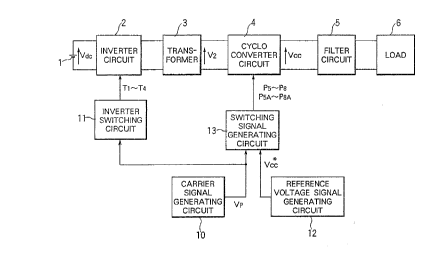
As shown in Fig. 1, a power conversion apparatus
according to a first embodiment of the present invention is
arranged in such a manner that a switching signal generating
circuit 13 is employed in place of the switching signal
generating circuit 13b employed in the conventional power
conversion apparatus shown in Fig. 8.
As shown in Fig. 2, the switching signal generating
circuit 13 comprises an absolute value circuit 102, a
comparator 103, NOT circuits 105, 106, 108 and 110, 1/2
dividers 104 and 107, a polarity discriminating circuit 109,
AND circuits 111 to 118 and OR circuits 119 to 126 so
20~33gl
that switching signals P5 to P8 and P5A to P8A are ~
transmitted. The above-described switching signals are
respectively supplied to the corresponding switching
devices S5 to S8 and S5A to S8A of the cyclo converter
circuit 4.
The operation of the first embodiment of the
present invention thus-constituted will now be described
with reference to a timing chart shown in Fig. 3. When the
sawtooth shape carrier signal Vp facing an upper right
direction is first transmitted from the carrier signal
generating circuit 10, the signal Tx and Ty, the duty ratio
of each of which is 50%, are supplied from the inverter
switching circuit 11 to the inverter circuit 2 as the
switching signals Tl to T4 similarly to the conventional
structure shown in Fig. 8. As a result, the rectangular
voltage V2, the duty ratio of which is 50%, is transmitted
from the transformer 3.
On the other hand, the reference voltage signal
generating circuit 12 transmits the reference voltage
signal Vcc* to be transmitted from the cyclo converter 4,
the reference voltage signal Vcc* being, together with the
carrier signal Vp, supplied to the switching signal
generating circuit 13. The switching signal generating
circuit 13 receives the above-described signals so as to
transmit the switching signals Ts to Ts the pulse width of
l4
205 3 3~ ~
each which has been modulated as follows. Referring to
Fig. 11, the reference voltage signal Vcc* is converted
into the absolute signal IVcc*l by the absolute value
circuit 102. The absolute signal IVCC*I is, together with
the carrier signal Vp, supplied to the comparator 103. The
comparator 103 transmits the signal Tp shown in Fig. 12,
the signal Tp being then supplied to the 1/2 divider 104 in
which the signal Tp is converted into the signal Ta. On
the other hand, when the signal Tp is supplied to the 1/2
divider 107 after the sign of it has been inverted by the
NOT circuit 106, the signal Tb formed into the same wave
shape as that of the signal Tx is transmitted.
Furthermore, when the signal Ta is supplied to the NOT
circuit 105, the signal Tc is transmitted, while when the
signal Tb is supplied to the NOT circuit 108, the signal Td
formed into the same wave shape as that of the signal Ty is
transmitted.
Furthermore, the polarity discriminating circuit 109
transmits the polarity signal Vsgn denoting the polarity of
the reference voltage signal Vcc. In addition, the NOT
circuit 110 transmits a signal which is a signal obtainable
by inverting the sign of the polarity signal Vsgn. The
above-described signals and the signals Ta to Td are, via
the AND circuits 111 to 118, supplied to the OR circuits
119 to 122. In accordance with the polarity of the
-l5-
2~33~
reference voltage signal Vcc, the signals Ts to Ts expressed
by the above-described Equation B or D are respectively
transmitted from the OR circuits 119 to 122.
As a result, the logical sum of the signals Ts and Td
is calculated in the OR circuit 123 so that the switching
signal Ps shown in Fig. 3 is generated so as to be supplied
to the switching device S5 of the cyclo converter circuit
4. Similarly, the logical sum of the signals Ts and Tb,
that of the signals T6 and Td and that of the signals T6 and
Tb are calculated in the OR circuits 124 to 126 so that the
switching signal P5A, P6 and P6A are generated so as to be
supplied to the switching devices S5A, S6 and S6A.
The signal T7 is as it is supplied to the switching
devices S7 and S7A as the switching signals P7 and P7A.
Furthermore, the signal Ts is as it is supplied to the
switching devices Ss and S8A as the switching signals Ps and
P8A.
The operation performed at time t2 shown in Fig.
3 will now be described. At this time, the status in which
the polarity of the voltage V2 has been positive, the
switches Qs and Qs have been switched on and the cyclo
converter circuit 4 has been transmitting positive voltage
is being changed to a status in which the switch Qs is
switched off, the switches Q6 and Q8 are switched on and the
cyclo converter circuit 4 transmits zero voltage. An
l6-
2Q~ 33~.L
assumption is made here that the electric current passes in
a positive direction through a route composed of the
switching device Ss, the diode D5A, the filter circuit 5,
the load circuit 6, the switching device S8 and the diode
D8A in this sequential order. When the switching device S5
is switched off in this state, passing of the electric
current is continued due to the portion of the inductance
of each of the filter circuit 5 and the load circuit 6.
However, since the switching-on signal has been supplied to
the switching device S6A at this time, the above-described
current is shifted to the switches S6A-D6 so as to be
circulated. Therefore, the electric current passing
through the portion corresponding to the inductance is not
cut off. Furthermore, no surge voltage is generated.
Therefore, the necessity of using the great capacity
snubber circuit for absorbing the surge voltage can be
eliminated.
A second embodiment of the present invention
will now be described with reference to Figs. 4 to 7.
Fig. 4 is a structural view which illustrates a second
embodiment of the present invention. Referring to Fig. 4,
reference numeral 4a represents a three-phase cyclo
converter circuit and 5a represents a three-phase filter
circuit connected to the output terminal of the three-phase
cyclo converter circuit 4a. Reference numeral 6a
20~338~
represents a three-phase load circuit connected to the
output terminal of the three-phase filter circuit 5a.
Reference numeral 12a represents a three-phase reference
voltage signal generating circuit for generating a signal
denoting the reference voltage which serves as a reference
of the output voltage from the cyclo converter circuit 4a.
Reference numeral 13a represents a switching signal
generating circuit of the cyclo converter.
Fig. 5 is a structural view which illustrates the
detailed structures of the cyclo converter circuit 4a and
the filter circuit 5a. The cyclo converter circuit 4a
comprises switching devices Ss to Slo and S5A to S10A, diodes
D5 to Dlo and D5A to D10A connected to the above-described
switching devices S5 to Slo and S5A to S10A in an anti-
parallel manner. The filter circuit Sa is composed of
three reaCtQrS LF and three capacitors CF.
Fig. 6 is a block diagram which illustrates the
detailed structure of the switching signal generating
circuit 13a. Referring to Fig. 6, reference numerals 201
to 203 represent comparators and 204 to 206 and 211
represent 1/2 dividers which transmit output signals the
polarity of each of which is inverted in synchronization
with the last transition of the input signal. Reference
numerals 207 to 210 and 212 represent NOT circuits and 213
to 224 represent OR circuits.
--l8--
2~i33'~
The operation of the second embodiment will now
be described with reference to a timing chart shown in Fig.
7.
Similarly to the first embodiment, the rectangular
voltage V2, the duty ratio of which is 50% and which
synchronizes with the carrier signal Vp, is transmitted
from the transformer 3. On the other hand, in the
switching signal generating circuit 13a, the carrier signal
Vp and three-phase reference voltage signals Vccu*, Vccv*
and Vccw* transmitted from the reference voltage signal
generating circuit 12a are subjected to comparisons by the
comparators 201 to 203 so that signals Tpu to Tpw are
formed. The u-phase 1/2 divider 204 converts the signal
Tpu into the signal Ts before the polarity of it is
inverted by the NOT circuit 207 so that the signal T6 shown
in Fig. 7 is obtained. In the 1/2 divider 211 to which the
w-phase signal Tpw has been supplied after its polarity had
been inverted by the NOT circuit 210, the signal Tb which
synchronizes with the carrier signal Vp is obtained. The
polarity of the signal Tb is then inverted by the NOT
circuit 212 so that the signal Td is obtained.
As a result, the logical sum of the signals Ts and Td
is calculated in the OR circuit 213 so that the switching
signal P5 shown in Fig. 7 is generated so as to be supplied
to the switching device S5 of the cyclo converter circuit
_ 1 9 _
- 2 ~
,
4a. Similarly, the logical sum of the signals Ts and Tb,
that of the signals T6 and Td and that of the signals T6 and
Tb are calculated in the OR circuits 214 to 216 so that the
switching signals P5A~ P6, and P6A are generated so as to be
supplied to the switching devices S5A, S6 and S6A.
Similarly to the u-phase, the switching signals P7,
P7A, P8 and P8A are supplied to the v-phase switching devices
S7, S7A, Ss and S8A from the OR circuits 217 to 220.
Switching signals Ps, P9A, P1o and P10A are supplied to w-
phase switching devices Ss, S9A, S10 and S10A from the OR
circuits 221 to 224.
The operation to be performed at time t3 shown
in Fig. 7 will now be described. At this time, a status in
which the polarity of the voltage V2 iS positive, the
switch Qs has been switched on so that positive voltage
Vccu is transmitted on the basis of an imaginary neutral
point, for example, the middle point of the secondary coil
of the transformer 3 is being shifted to a status in which
the switch Qs is switched off and as well as the switch Q6
is switched on so that negative voltage Vccu is
transmitted. An assumption is made here that the electric
current passes in a positive direction from the switching
device Ss-diode D5A to the filter circuit 5a at this time.
When the switch Qs is switched off in this state, the
electric current which has passed through the switching
-20-
- 2~3~
device S5 iS shifted to the switch S6A-D6 to which the
switching-on signal has been supplied at this time.
Therefore, the electric current passing through the
portion corresponding to the inductance of the filter
circuit 5a and the load circuit 6a is not cut off.
Furthermore, no surge voltage is generated. Therefore, the
necessity of using the great capacity snubber circuit for
absorbing the surge voltage can be eliminated. Also at the
other timing and in the other phases, the mode in which the
passage for the electric current is opened can be
eliminated so that similar effects can be obtained.
According to the above-described embodiments, the
switch for the cyclo converter is constituted by the
switching devices and the dioded. However, the present
invention is not limited to this. Therefore, any switch
which is capable of controlling the direction of the
electric current may be employed to obtain the effect
obtainable from the above-described embodiments.
21