Language selection

Search

Patent 2053382 Summary

Third-party information liability

Some of the information on this Web page has been provided by external sources. The Government of Canada is not responsible for the accuracy, reliability or currency of the information supplied by external sources. Users wishing to rely upon this information should consult directly with the source of the information. Content provided by external sources is not subject to official languages, privacy and accessibility requirements.

Claims and Abstract availability

Any discrepancies in the text and image of the Claims and Abstract are due to differing posting times. Text of the Claims and Abstract are posted:
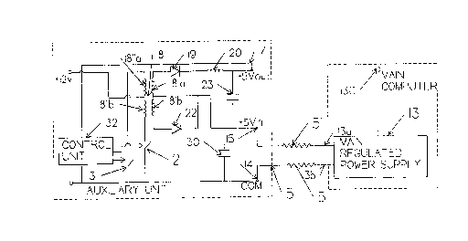
  • At the time the application is open to public inspection;
  • At the time of issue of the patent (grant).
(12) Patent: (11) CA 2053382
(54) English Title: VOLTAGE BOOSTER
(54) French Title: SURVOLTEUR
Status: Expired
Bibliographic Data
(51) International Patent Classification (IPC):
  • G05F 1/10 (2006.01)
  • G05F 1/56 (2006.01)
  • G06F 1/30 (2006.01)
  • H02M 3/335 (2006.01)
(72) Inventors :
  • LAVRISA, TOM (Canada)
(73) Owners :
  • MITEL NETWORKS CORPORATION (Not Available)
(71) Applicants :
(74) Agent: MARKS & CLERK
(74) Associate agent:
(45) Issued: 2000-04-18
(22) Filed Date: 1991-10-11
(41) Open to Public Inspection: 1993-04-12
Examination requested: 1997-07-08
Availability of licence: N/A
(25) Language of filing: English

Patent Cooperation Treaty (PCT): No

(30) Application Priority Data: None

Abstracts

English Abstract


An auxiliary regulated power supply is described for
use in a system having a main load directly connected to a
main regulated power supply and an auxiliary load connected
to the main regulated power supply by a line in which a
voltage drop occurs. The auxiliary regulated power supply
comprises a pair of input terminals for connection to the
line, a pair of terminals far connection to a voltage
source, a pair of output terminals for connection to the
auxiliary load, a circuit for sensing the voltage at the
output terminals, and an arrangement for boosting the output
voltage at the output terminals from a secondary voltage
source as necessary to maintain it at a level appropriate
for the auxiliary load.


Claims

Note: Claims are shown in the official language in which they were submitted.


THE EMBODIMENTS OF THE INVENTION IN WHICH AN EXCLUSIVE
PROPERTY OR PRIVILEGE IS CLAIMED ARE DEFINED AS FOLLOWS:
1. In a system comprising a main load directly connected
to a main regulated power supply and an auxiliary load
connected to said main regulated power supply by a line in
which a voltage drop occurs, said main regulated supply
being connected at a near end of said line, and an auxiliary
regulated power supply being connected at a far end of said
line, said auxiliary regulated power supply comprising:
a pair of input terminals connected to said far end of said
line and receiving an input voltage therefrom;
a secondary voltage source;
a pair of secondary terminals connected to said secondary
voltage source;
a pair of output terminals connected to said auxiliary load
and supplying an output voltage;
means for adding voltage from said secondary voltage source
to said input voltage to provide said output voltage;
means for applying said output voltage to said output
terminals; and
control means for sensing the voltage at said output
terminals, said control means being operative to control
said adding means in a feedback arrangement to maintain said
output voltage at a constant level appropriate for said
auxiliary load.
2. A system as claimed in claim 1, wherein said adding
means comprises a buck converter for adding voltage to the
voltage appearing at said pair of input terminals to
maintain said output voltage at the appropriate level.
3. A system as claimed in claim 2, wherein said buck
converter is a forward converter.


4. A system supply as claimed in claim 2, wherein said
buck converter is a push-pull converter.
5. A system supply as claimed in claim 2, wherein the buck
converter comprises a switching transistor connected in
series with an inductance across said voltage source, diode
means and capacitor means for supplying smoothed extra
voltage to said auxiliary output, said switching transistor
being controlled according to the voltage boosting
requirements of the output voltage.
6. A system as claimed in claim 5, wherein the inductance
is included in a transformer coupling the voltage source to
the auxiliary output.
7. A system as claimed in claim 1, wherein said
appropriate level is the same as the regulated voltage
provided by the main power supply.
8. A system as claimed in claim 1, wherein said voltage
source is provided by the main power supply.

Description

Note: Descriptions are shown in the official language in which they were submitted.


~(~~~t~~>
This invention relates to a regulated auxiliary power
supply for use with personal computers and similar
electronic equipment.
A personal computer includes a regulated power supply
which produces the required supply voltage, normally 5
Volts, for the various loads within the computer. Such
power supplies generally provide a 12 Volt output in
addition. The power supply is regulated to maintain a
constant voltage as the current requirements vary. A
problem arises when it is desired to drive a remote terminal
from the same power supply or to include circuitry in the
computer that must be powered redundantly from two separate
systems. If the supply is regulated according to the
requirements of the main computer components, in the first
case the voltage drop along the supply lead reduces the
voltage at the auxiliary output, and in the second case the
voltage at the auxiliary output is reduced by the series
isolation diodes required to separate the two systems.
An object of the invention is to provide a regulated
power supply capable of overcoming the aforementioned
disadvantages.
According to the present invention there is provided an
auxiliary regulated power supply for use in a system having
a main load directly connected to a main regulated power
supply and an auxiliary load connected to the main regulated
power supply by a line in which a voltage drop occurs, said
auxiliary regulated power supply comprising a pair of input
terminals for connection to said line, a pair of terminals
for connection to a secondary voltage source, a pair of
output terminals for connection to the auxiliary load, means
for sensing the voltage at the output terminals, and means
for boosting the output voltage at said output terminals
from said voltage source as necessary to maintain said
- 1 -

1
2~~~?~~
output voltage at a level appropriate for said auxiliary
load.
Preferably, the means for boosting the output voltage
is a forward converter. At higher currents a push-pull
converter may advantageously be employed.
By boosting voltage at the output terminals in this
manner, a stable five volt with minimum current ripple can
be readily maintained at the auxiliary output. Each ampere
of current drawn from the main power supply generates one
ampere of output current at the auxiliary output at the
desired voltage, normally five volts.
The invention also provides a method of providing an
auxiliary voltage regulated output for connection to an
auxiliary load that is connected to a main regulated power
supply over a line in which a voltage drop occurs,
comprising sensing the voltage across said auxiliary load,
and boosting said voltage from a secondary voltage source as
necessary to maintain it at the appropriate level.
The invention will now be described in more detail, by
way of example, with reference to the accompanying drawings,
in which:
Figure 1 shows a personal computer connected to a
remote terminal running off a common power supply;
Figure 2 shows an alternative arrangement where a
circuit is powered redundantly from two separate systems;
Figure 3 shows a known boost converter circuit;
Figure 4 shows an arrangement in accordance with the
invention for providing an auxiliary regulated power supply
- 2 -


2~~~~~>
employing a forward converter; and
Figure 5 shows an arrangement in accordance wit#~ the
invention for providing an auxiliary regulated power supply
employing a push-pull converter.
Referring now to Figure 1, personal computer 1
comprises an internal regulated power supply 2, which drives
a CPU 3 and other standard components (not shown). The
computer 1 is connected to a remote terrainal 4, which is
driven by the same power supply 2 as the computer 1 over a
lossy line 5, which causes a voltage drop across it.
A problem is that if the power supply is properly
regulated for the CPU of the computer 1, the voltage drop
across line 5 connecting the computer 1 to the terminal ~
causes the voltage applied to the remote terminal to become
too low and consequently no longer regulated.
Figure 2 shows an alternative situation where a load 6
is required to be driven redundantly from separate power
supplies 2 of computers 1, 1', which are respectively
connected to the load 6 through isolation diodes 7, 8. The
voltage drop across the isolation diodes causes the voltage
to be applied to the load 6 to become too low. In theory,
it might be considered possible to boost the voltage as seen
by the input of the auxiliary load with a classic boost
convertor of the type shown in Figure 3.
In the arrangement shown in Figure 3 an input voltage
is applied across a series combination of an inductance 9
and high speed switch 10, which in practice is a transistor.
The inductance 9 acts as a current source. The current in
inductance 9 ramps up when transistor 10 is on and ramps
down through the diode il when the transistor 10 is off. A
steady voltage appears at the output.
- 3 -


zu~~~~~
A drawback with this type of circuit, however, is that
it is difficult to make it work with a nominal + 5 volt
input voltage, which is the most common voltage requirement
fox computers and similar equipment. Also, this circuit
produces a high ripple current.
Referring now to Figure 4, a conventional regulated
main power supply circuit 13, supplies a regulated 5 Volt
output at a main output defined by terminals 13a, 13b and in
addition a 12 Volt output at terminal 13c. Power supply,
circuit 13 may be, for example, the main power supply of a
personal computer. Alternatively, the voltage drop can be '
caused by isolation diodes, as shown in Figure 2. The
isolation diode can be placed as shown in Figure 4 as 99 in
broken lines. Power supply 13 is connected to input
terminals 14, 15 of the auxiliary circuit by a line 5
including loss resistance 5', which causes a voltage drop in
the line.
An auxiliary regulated output defined by terminals 14,
17 is derived from the voltage appearing at terminals 14,
15. Terminal 15 is connected to terminal 17 through
inductance 18' forming a secondary winding of transformer
18, diode 19 and inductance 20, and also parallel diode 22.
Smoothing capacitor 30 is connected across the input
teriminals 14, 15.
Primary winding 18~~ of transformer 18 is connected to a
12 volt supply, which can conveniently be provided by the
main power supply 13 through terminal 13c, in series with
switch 21, which in practice is a high speed transistor
driven by a control circuit 32 in dependence on the voltage
at output terminal 17. Control circuit 32 is a pulse width
modulated control circuit, for example having a UC3845
integrated circuit manufactured by Unitrode, or Motorola.
The duty cycle of the transistor 21 is adjusted to maintain
- 4 -


.. ~~.3La~~N
the desired 5 volts at output terminal 17 regardless of the
current drawn by the auxiliary load (not shown) across
terminals 14, 17. Each ampere of current drawn on the 5
volt input generates one ampere of 5 volt output current,
with the extra power being taken from the 12 volt source.
This extra power also overcomes any losses in the convertor
itself. The transformer 18 also includes a clamp winding
18 " ' in series with a diode 25 to limit the voltage
developed across switch 21.
The rapid operation of high speed switch 21 causes a
current to be induced in inductance 20, which ramps up when
the transistor 21 is on and down when it is off. Capacitor
23 acts as a smoothing capacitor to minimize ripple. The
net effect of the circuit is to produce a regulated 5 Volt
output at terminals 14, 17, which consists of the voltage
appearing at terminals 14, 15 boosted as necessary by extra
voltage derived from the 12 Volt supply.
Figure 5 shows an arrangement including a push-pull
buck converter circuit. Similar components have similar
reference numerals to Figure 4. In Figure 5, the primary
and secondary windings of transformer 18' are split into
half-windings 18'a, 18'b, and 18"a, 18"c respectively, which
are provided in a,push-pull arrangement. Terminal 15 is
connected to the common point of windings 18'a and 18°b, and
the common point of half-windings 18"a, 18"b is connected to
the 12V supply. Diode 25 is replaced by a switch 31
controlled by the control circuit 32.
The push-pull arrangement is useful at higher currents.
While many circuits can be employed to generate the
added voltage for the auxiliary output, buck derived
circuits are preferred in view of their low ripple current
on the output capacitor.
- 5 -

Representative Drawing
A single figure which represents the drawing illustrating the invention.
Administrative Status

For a clearer understanding of the status of the application/patent presented on this page, the site Disclaimer , as well as the definitions for Patent , Administrative Status , Maintenance Fee  and Payment History  should be consulted.

Administrative Status

Title Date
Forecasted Issue Date 2000-04-18
(22) Filed 1991-10-11
(41) Open to Public Inspection 1993-04-12
Examination Requested 1997-07-08
(45) Issued 2000-04-18
Expired 2011-10-11

Abandonment History

There is no abandonment history.

Payment History

Fee Type Anniversary Year Due Date Amount Paid Paid Date
Application Fee $0.00 1991-10-11
Registration of a document - section 124 $0.00 1992-05-22
Maintenance Fee - Application - New Act 2 1993-10-11 $100.00 1993-07-15
Maintenance Fee - Application - New Act 3 1994-10-11 $100.00 1994-08-05
Maintenance Fee - Application - New Act 4 1995-10-11 $100.00 1995-09-28
Maintenance Fee - Application - New Act 5 1996-10-11 $150.00 1996-09-05
Request for Examination $400.00 1997-07-08
Maintenance Fee - Application - New Act 6 1997-10-14 $150.00 1997-10-06
Registration of a document - section 124 $50.00 1998-02-16
Maintenance Fee - Application - New Act 7 1998-10-13 $150.00 1998-09-29
Maintenance Fee - Application - New Act 8 1999-10-11 $150.00 1999-08-25
Final Fee $300.00 2000-01-13
Maintenance Fee - Patent - New Act 9 2000-10-11 $150.00 2000-07-31
Registration of a document - section 124 $50.00 2001-04-24
Registration of a document - section 124 $50.00 2001-05-04
Maintenance Fee - Patent - New Act 10 2001-10-11 $200.00 2001-08-09
Maintenance Fee - Patent - New Act 11 2002-10-11 $200.00 2002-09-19
Maintenance Fee - Patent - New Act 12 2003-10-13 $200.00 2003-09-17
Maintenance Fee - Patent - New Act 13 2004-10-11 $250.00 2004-09-09
Registration of a document - section 124 $100.00 2005-07-11
Registration of a document - section 124 $100.00 2005-07-18
Maintenance Fee - Patent - New Act 14 2005-10-11 $250.00 2005-09-08
Maintenance Fee - Patent - New Act 15 2006-10-11 $450.00 2006-09-08
Maintenance Fee - Patent - New Act 16 2007-10-11 $450.00 2007-09-07
Registration of a document - section 124 $100.00 2007-09-14
Maintenance Fee - Patent - New Act 17 2008-10-13 $450.00 2008-09-15
Registration of a document - section 124 $100.00 2009-02-24
Maintenance Fee - Patent - New Act 18 2009-10-12 $450.00 2009-09-14
Registration of a document - section 124 $100.00 2010-01-14
Maintenance Fee - Patent - New Act 19 2010-10-11 $450.00 2010-09-16
Owners on Record

Note: Records showing the ownership history in alphabetical order.

Current Owners on Record
MITEL NETWORKS CORPORATION
Past Owners on Record
LAVRISA, TOM
MITEL CORPORATION
MITEL KNOWLEDGE CORPORATION
Past Owners that do not appear in the "Owners on Record" listing will appear in other documentation within the application.
Documents

To view selected files, please enter reCAPTCHA code :


To view images, click a link in the Document Description column. To download the documents, select one or more checkboxes in the first column and then click the "Download Selected in PDF format (Zip Archive)" or the "Download Selected as Single PDF" button.

List of published and non-published patent-specific documents on the CPD .

If you have any difficulty accessing content, you can call the Client Service Centre at 1-866-997-1936 or send them an e-mail at CIPO Client Service Centre.


Document
Description 
Date
(yyyy-mm-dd) 
Number of pages   Size of Image (KB) 
Cover Page 2000-03-16 1 33
Cover Page 1994-02-19 1 13
Abstract 1994-02-19 1 20
Claims 1994-02-19 2 70
Drawings 1994-02-19 3 51
Description 1994-02-19 5 210
Claims 1999-08-17 2 69
Representative Drawing 1999-08-05 1 14
Representative Drawing 2000-03-16 1 10
Assignment 2001-04-24 37 2,277
Assignment 1998-02-16 32 1,528
Assignment 1991-10-11 5 132
Prosecution-Amendment 1997-07-08 1 36
Prosecution-Amendment 1999-08-17 4 110
Correspondence 2000-01-13 1 30
Prosecution-Amendment 1999-02-17 2 3
Correspondence 2000-10-03 1 15
Assignment 2001-05-04 13 780
Assignment 2001-06-13 2 98
Assignment 2005-07-11 70 4,393
Assignment 2005-07-18 42 3,905
Assignment 2007-09-14 39 2,305
Assignment 2007-09-14 39 2,319
Assignment 2009-02-24 12 749
Assignment 2010-01-14 12 738
Assignment 2010-01-13 51 2,926
Fees 1996-09-05 1 51
Fees 1995-09-28 1 53
Fees 1994-08-05 1 70
Fees 1993-07-15 1 35