Sélection de la langue

Search

Sommaire du brevet 2053382 

Énoncé de désistement de responsabilité concernant l'information provenant de tiers

Une partie des informations de ce site Web a été fournie par des sources externes. Le gouvernement du Canada n'assume aucune responsabilité concernant la précision, l'actualité ou la fiabilité des informations fournies par les sources externes. Les utilisateurs qui désirent employer cette information devraient consulter directement la source des informations. Le contenu fourni par les sources externes n'est pas assujetti aux exigences sur les langues officielles, la protection des renseignements personnels et l'accessibilité.

Disponibilité de l'Abrégé et des Revendications

L'apparition de différences dans le texte et l'image des Revendications et de l'Abrégé dépend du moment auquel le document est publié. Les textes des Revendications et de l'Abrégé sont affichés :

  • lorsque la demande peut être examinée par le public;
  • lorsque le brevet est émis (délivrance).
(12) Brevet: (11) CA 2053382
(54) Titre français: SURVOLTEUR
(54) Titre anglais: VOLTAGE BOOSTER
Statut: Périmé
Données bibliographiques
Abrégés

Abrégé anglais


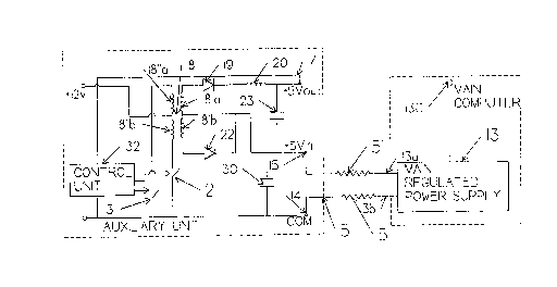
An auxiliary regulated power supply is described for
use in a system having a main load directly connected to a
main regulated power supply and an auxiliary load connected
to the main regulated power supply by a line in which a
voltage drop occurs. The auxiliary regulated power supply
comprises a pair of input terminals for connection to the
line, a pair of terminals far connection to a voltage
source, a pair of output terminals for connection to the
auxiliary load, a circuit for sensing the voltage at the
output terminals, and an arrangement for boosting the output
voltage at the output terminals from a secondary voltage
source as necessary to maintain it at a level appropriate
for the auxiliary load.

Revendications

Note : Les revendications sont présentées dans la langue officielle dans laquelle elles ont été soumises.


THE EMBODIMENTS OF THE INVENTION IN WHICH AN EXCLUSIVE
PROPERTY OR PRIVILEGE IS CLAIMED ARE DEFINED AS FOLLOWS:
1. In a system comprising a main load directly connected
to a main regulated power supply and an auxiliary load
connected to said main regulated power supply by a line in
which a voltage drop occurs, said main regulated supply
being connected at a near end of said line, and an auxiliary
regulated power supply being connected at a far end of said
line, said auxiliary regulated power supply comprising:
a pair of input terminals connected to said far end of said
line and receiving an input voltage therefrom;
a secondary voltage source;
a pair of secondary terminals connected to said secondary
voltage source;
a pair of output terminals connected to said auxiliary load
and supplying an output voltage;
means for adding voltage from said secondary voltage source
to said input voltage to provide said output voltage;
means for applying said output voltage to said output
terminals; and
control means for sensing the voltage at said output
terminals, said control means being operative to control
said adding means in a feedback arrangement to maintain said
output voltage at a constant level appropriate for said
auxiliary load.
2. A system as claimed in claim 1, wherein said adding
means comprises a buck converter for adding voltage to the
voltage appearing at said pair of input terminals to
maintain said output voltage at the appropriate level.
3. A system as claimed in claim 2, wherein said buck
converter is a forward converter.


4. A system supply as claimed in claim 2, wherein said
buck converter is a push-pull converter.
5. A system supply as claimed in claim 2, wherein the buck
converter comprises a switching transistor connected in
series with an inductance across said voltage source, diode
means and capacitor means for supplying smoothed extra
voltage to said auxiliary output, said switching transistor
being controlled according to the voltage boosting
requirements of the output voltage.
6. A system as claimed in claim 5, wherein the inductance
is included in a transformer coupling the voltage source to
the auxiliary output.
7. A system as claimed in claim 1, wherein said
appropriate level is the same as the regulated voltage
provided by the main power supply.
8. A system as claimed in claim 1, wherein said voltage
source is provided by the main power supply.

Description

Note : Les descriptions sont présentées dans la langue officielle dans laquelle elles ont été soumises.


~(~~~t~~>
This invention relates to a regulated auxiliary power
supply for use with personal computers and similar
electronic equipment.
A personal computer includes a regulated power supply
which produces the required supply voltage, normally 5
Volts, for the various loads within the computer. Such
power supplies generally provide a 12 Volt output in
addition. The power supply is regulated to maintain a
constant voltage as the current requirements vary. A
problem arises when it is desired to drive a remote terminal
from the same power supply or to include circuitry in the
computer that must be powered redundantly from two separate
systems. If the supply is regulated according to the
requirements of the main computer components, in the first
case the voltage drop along the supply lead reduces the
voltage at the auxiliary output, and in the second case the
voltage at the auxiliary output is reduced by the series
isolation diodes required to separate the two systems.
An object of the invention is to provide a regulated
power supply capable of overcoming the aforementioned
disadvantages.
According to the present invention there is provided an
auxiliary regulated power supply for use in a system having
a main load directly connected to a main regulated power
supply and an auxiliary load connected to the main regulated
power supply by a line in which a voltage drop occurs, said
auxiliary regulated power supply comprising a pair of input
terminals for connection to said line, a pair of terminals
for connection to a secondary voltage source, a pair of
output terminals for connection to the auxiliary load, means
for sensing the voltage at the output terminals, and means
for boosting the output voltage at said output terminals
from said voltage source as necessary to maintain said
- 1 -

1
2~~~?~~
output voltage at a level appropriate for said auxiliary
load.
Preferably, the means for boosting the output voltage
is a forward converter. At higher currents a push-pull
converter may advantageously be employed.
By boosting voltage at the output terminals in this
manner, a stable five volt with minimum current ripple can
be readily maintained at the auxiliary output. Each ampere
of current drawn from the main power supply generates one
ampere of output current at the auxiliary output at the
desired voltage, normally five volts.
The invention also provides a method of providing an
auxiliary voltage regulated output for connection to an
auxiliary load that is connected to a main regulated power
supply over a line in which a voltage drop occurs,
comprising sensing the voltage across said auxiliary load,
and boosting said voltage from a secondary voltage source as
necessary to maintain it at the appropriate level.
The invention will now be described in more detail, by
way of example, with reference to the accompanying drawings,
in which:
Figure 1 shows a personal computer connected to a
remote terminal running off a common power supply;
Figure 2 shows an alternative arrangement where a
circuit is powered redundantly from two separate systems;
Figure 3 shows a known boost converter circuit;
Figure 4 shows an arrangement in accordance with the
invention for providing an auxiliary regulated power supply
- 2 -


2~~~~~>
employing a forward converter; and
Figure 5 shows an arrangement in accordance wit#~ the
invention for providing an auxiliary regulated power supply
employing a push-pull converter.
Referring now to Figure 1, personal computer 1
comprises an internal regulated power supply 2, which drives
a CPU 3 and other standard components (not shown). The
computer 1 is connected to a remote terrainal 4, which is
driven by the same power supply 2 as the computer 1 over a
lossy line 5, which causes a voltage drop across it.
A problem is that if the power supply is properly
regulated for the CPU of the computer 1, the voltage drop
across line 5 connecting the computer 1 to the terminal ~
causes the voltage applied to the remote terminal to become
too low and consequently no longer regulated.
Figure 2 shows an alternative situation where a load 6
is required to be driven redundantly from separate power
supplies 2 of computers 1, 1', which are respectively
connected to the load 6 through isolation diodes 7, 8. The
voltage drop across the isolation diodes causes the voltage
to be applied to the load 6 to become too low. In theory,
it might be considered possible to boost the voltage as seen
by the input of the auxiliary load with a classic boost
convertor of the type shown in Figure 3.
In the arrangement shown in Figure 3 an input voltage
is applied across a series combination of an inductance 9
and high speed switch 10, which in practice is a transistor.
The inductance 9 acts as a current source. The current in
inductance 9 ramps up when transistor 10 is on and ramps
down through the diode il when the transistor 10 is off. A
steady voltage appears at the output.
- 3 -


zu~~~~~
A drawback with this type of circuit, however, is that
it is difficult to make it work with a nominal + 5 volt
input voltage, which is the most common voltage requirement
fox computers and similar equipment. Also, this circuit
produces a high ripple current.
Referring now to Figure 4, a conventional regulated
main power supply circuit 13, supplies a regulated 5 Volt
output at a main output defined by terminals 13a, 13b and in
addition a 12 Volt output at terminal 13c. Power supply,
circuit 13 may be, for example, the main power supply of a
personal computer. Alternatively, the voltage drop can be '
caused by isolation diodes, as shown in Figure 2. The
isolation diode can be placed as shown in Figure 4 as 99 in
broken lines. Power supply 13 is connected to input
terminals 14, 15 of the auxiliary circuit by a line 5
including loss resistance 5', which causes a voltage drop in
the line.
An auxiliary regulated output defined by terminals 14,
17 is derived from the voltage appearing at terminals 14,
15. Terminal 15 is connected to terminal 17 through
inductance 18' forming a secondary winding of transformer
18, diode 19 and inductance 20, and also parallel diode 22.
Smoothing capacitor 30 is connected across the input
teriminals 14, 15.
Primary winding 18~~ of transformer 18 is connected to a
12 volt supply, which can conveniently be provided by the
main power supply 13 through terminal 13c, in series with
switch 21, which in practice is a high speed transistor
driven by a control circuit 32 in dependence on the voltage
at output terminal 17. Control circuit 32 is a pulse width
modulated control circuit, for example having a UC3845
integrated circuit manufactured by Unitrode, or Motorola.
The duty cycle of the transistor 21 is adjusted to maintain
- 4 -


.. ~~.3La~~N
the desired 5 volts at output terminal 17 regardless of the
current drawn by the auxiliary load (not shown) across
terminals 14, 17. Each ampere of current drawn on the 5
volt input generates one ampere of 5 volt output current,
with the extra power being taken from the 12 volt source.
This extra power also overcomes any losses in the convertor
itself. The transformer 18 also includes a clamp winding
18 " ' in series with a diode 25 to limit the voltage
developed across switch 21.
The rapid operation of high speed switch 21 causes a
current to be induced in inductance 20, which ramps up when
the transistor 21 is on and down when it is off. Capacitor
23 acts as a smoothing capacitor to minimize ripple. The
net effect of the circuit is to produce a regulated 5 Volt
output at terminals 14, 17, which consists of the voltage
appearing at terminals 14, 15 boosted as necessary by extra
voltage derived from the 12 Volt supply.
Figure 5 shows an arrangement including a push-pull
buck converter circuit. Similar components have similar
reference numerals to Figure 4. In Figure 5, the primary
and secondary windings of transformer 18' are split into
half-windings 18'a, 18'b, and 18"a, 18"c respectively, which
are provided in a,push-pull arrangement. Terminal 15 is
connected to the common point of windings 18'a and 18°b, and
the common point of half-windings 18"a, 18"b is connected to
the 12V supply. Diode 25 is replaced by a switch 31
controlled by the control circuit 32.
The push-pull arrangement is useful at higher currents.
While many circuits can be employed to generate the
added voltage for the auxiliary output, buck derived
circuits are preferred in view of their low ripple current
on the output capacitor.
- 5 -

Dessin représentatif
Une figure unique qui représente un dessin illustrant l'invention.
États administratifs

Pour une meilleure compréhension de l'état de la demande ou brevet qui figure sur cette page, la rubrique Mise en garde , et les descriptions de Brevet , États administratifs , Taxes périodiques et Historique des paiements devraient être consultées.

États administratifs

Titre Date
Date de délivrance prévu 2000-04-18
(22) Dépôt 1991-10-11
(41) Mise à la disponibilité du public 1993-04-12
Requête d'examen 1997-07-08
(45) Délivré 2000-04-18
Expiré 2011-10-11

Historique d'abandonnement

Il n'y a pas d'historique d'abandonnement

Historique des paiements

Type de taxes Anniversaire Échéance Montant payé Date payée
Le dépôt d'une demande de brevet 0,00 $ 1991-10-11
Enregistrement de documents 0,00 $ 1992-05-22
Taxe de maintien en état - Demande - nouvelle loi 2 1993-10-11 100,00 $ 1993-07-15
Taxe de maintien en état - Demande - nouvelle loi 3 1994-10-11 100,00 $ 1994-08-05
Taxe de maintien en état - Demande - nouvelle loi 4 1995-10-11 100,00 $ 1995-09-28
Taxe de maintien en état - Demande - nouvelle loi 5 1996-10-11 150,00 $ 1996-09-05
Requête d'examen 400,00 $ 1997-07-08
Taxe de maintien en état - Demande - nouvelle loi 6 1997-10-14 150,00 $ 1997-10-06
Enregistrement de documents 50,00 $ 1998-02-16
Taxe de maintien en état - Demande - nouvelle loi 7 1998-10-13 150,00 $ 1998-09-29
Taxe de maintien en état - Demande - nouvelle loi 8 1999-10-11 150,00 $ 1999-08-25
Taxe finale 300,00 $ 2000-01-13
Taxe de maintien en état - brevet - nouvelle loi 9 2000-10-11 150,00 $ 2000-07-31
Enregistrement de documents 50,00 $ 2001-04-24
Enregistrement de documents 50,00 $ 2001-05-04
Taxe de maintien en état - brevet - nouvelle loi 10 2001-10-11 200,00 $ 2001-08-09
Taxe de maintien en état - brevet - nouvelle loi 11 2002-10-11 200,00 $ 2002-09-19
Taxe de maintien en état - brevet - nouvelle loi 12 2003-10-13 200,00 $ 2003-09-17
Taxe de maintien en état - brevet - nouvelle loi 13 2004-10-11 250,00 $ 2004-09-09
Enregistrement de documents 100,00 $ 2005-07-11
Enregistrement de documents 100,00 $ 2005-07-18
Taxe de maintien en état - brevet - nouvelle loi 14 2005-10-11 250,00 $ 2005-09-08
Taxe de maintien en état - brevet - nouvelle loi 15 2006-10-11 450,00 $ 2006-09-08
Taxe de maintien en état - brevet - nouvelle loi 16 2007-10-11 450,00 $ 2007-09-07
Enregistrement de documents 100,00 $ 2007-09-14
Taxe de maintien en état - brevet - nouvelle loi 17 2008-10-13 450,00 $ 2008-09-15
Enregistrement de documents 100,00 $ 2009-02-24
Taxe de maintien en état - brevet - nouvelle loi 18 2009-10-12 450,00 $ 2009-09-14
Enregistrement de documents 100,00 $ 2010-01-14
Taxe de maintien en état - brevet - nouvelle loi 19 2010-10-11 450,00 $ 2010-09-16
Titulaires au dossier

Les titulaires actuels et antérieures au dossier sont affichés en ordre alphabétique.

Titulaires actuels au dossier
MITEL NETWORKS CORPORATION
Titulaires antérieures au dossier
LAVRISA, TOM
MITEL CORPORATION
MITEL KNOWLEDGE CORPORATION
Les propriétaires antérieurs qui ne figurent pas dans la liste des « Propriétaires au dossier » apparaîtront dans d'autres documents au dossier.
Documents

Pour visionner les fichiers sélectionnés, entrer le code reCAPTCHA :


Pour visualiser une image, cliquer sur un lien dans la colonne description du document. Pour télécharger l'image (les images), cliquer l'une ou plusieurs cases à cocher dans la première colonne et ensuite cliquer sur le bouton "Télécharger sélection en format PDF (archive Zip)" ou le bouton "Télécharger sélection (en un fichier PDF fusionné)".

Liste des documents de brevet publiés et non publiés sur la BDBC .

Si vous avez des difficultés à accéder au contenu, veuillez communiquer avec le Centre de services à la clientèle au 1-866-997-1936, ou envoyer un courriel au Centre de service à la clientèle de l'OPIC.


Description du
Document 
Date
(yyyy-mm-dd) 
Nombre de pages   Taille de l'image (Ko) 
Page couverture 2000-03-16 1 33
Page couverture 1994-02-19 1 13
Abrégé 1994-02-19 1 20
Revendications 1994-02-19 2 70
Dessins 1994-02-19 3 51
Description 1994-02-19 5 210
Revendications 1999-08-17 2 69
Dessins représentatifs 1999-08-05 1 14
Dessins représentatifs 2000-03-16 1 10
Cession 2001-04-24 37 2 277
Cession 1998-02-16 32 1 528
Cession 1991-10-11 5 132
Poursuite-Amendment 1997-07-08 1 36
Poursuite-Amendment 1999-08-17 4 110
Correspondance 2000-01-13 1 30
Poursuite-Amendment 1999-02-17 2 3
Correspondance 2000-10-03 1 15
Cession 2001-05-04 13 780
Cession 2001-06-13 2 98
Cession 2005-07-11 70 4 393
Cession 2005-07-18 42 3 905
Cession 2007-09-14 39 2 305
Cession 2007-09-14 39 2 319
Cession 2009-02-24 12 749
Cession 2010-01-14 12 738
Cession 2010-01-13 51 2 926
Taxes 1996-09-05 1 51
Taxes 1995-09-28 1 53
Taxes 1994-08-05 1 70
Taxes 1993-07-15 1 35