Note: Descriptions are shown in the official language in which they were submitted.
253737
CONVERTER INPUT/OUTPUT VOLTAGE
BALANCING CONTROL
The present invention relates to a method and a circuit
arrangement for controlling power valves included in at least
one converter forming part of a converter coupling, which on
its input receives at least two DC voltages and transmits
current pulses corresponding respectively to these DC
voltages, to a common load via a common output filter, said
controlling aiming at keeping said DC voltages equal.
In pulse width modulated current-mode converters with a
pulse width of over 50 % of the cycle of a current pulse so
called slope compensation has to be resorted to for avoiding
unstable control of the converters. A closer description of
this can be obtained e.g. in "Application Note U-97" from the
company Unitrode having the title "Modelling, Analysis and
Compensation of the Current-Mode Controller". As will also
appear more closely from the description below slope
compensation shortly implies in the present case that the
control is carried through by means of a stop pulse for each
current pulse, said stop pulse being formed by the aid of a
ramp voltage. The ramps of the ramp voltage have a slope
opposite.to the slope of the current pulse ramps formed due to
the output filter, and appear with a cycle equal to the cycle
of the current pulse, corresponding to an input DC voltage,
divided by the number of input DC voltages. A further ramp
voltage is formed by subtraction of the first mentioned ramp
voltage from a pulse voltage proportional to the added current
pulses, corresponding to the input DC voltages, and the stop
pulse is generated each time the ramps of this further ramp
voltage reach a predetermined fixed voltage level.
It is important in an arrangement of the kind indicated by ,.
way of introduction that the input DC voltages are equal, i.e.
that no unbalance appears, since this can give rise to several
serious drawbacks. Small differences between the efficiencies
of e.g. two converters require the possibility of being able
2~~,~'~3'~
2
to adjust the power output from the converters individually.
It is also desirable that the frequency of the output
filter is as high as possible in order to be easy to be
filtered away. Thus it is desired that all pulses and all
pulse intervals shall be as equal as possible in order to make
only the sum frequency from all converters to appear in the
filter.
With unbalance is here meant that the input DC voltages
are unequal and that the converters feed the output filter
with current having a frequency spectrum containing a
frequency lower than that for which the filter is dimensioned.
Ripple appears on the output and disturbances on the input.
One of the converters can be overloaded and the other one
gives a considerably less power than that for which it is
intended. At worst one of the converters can get such a high
input voltage that it becomes defective. One form of unbalance
where the input voltages are equal but pulses and pulse
intervals are unequal, can also appear. In that case the
symptoms are limited to heavy disturbances on the input and
output.
State of the art.
A circuit arrangement of essentially the kind indicated
above by way of introduction is known through EP 0 162 374. In
this prior circuit arrangement the control is carried through
by changing the switched on times of the current converters so
that the relative deviations of the input DC voltages are
outbalanced if said deviations exceed a predetermined amount.
This solution is not able to take care of the case that one or
both of the input voltages sinks below a certain value, but
requires for this case the emergency solution that the
coupling arrangement is entirely switched off.
A further circuit arrangement of essentially the kind
indicated above by way of introduction is disclosed in US
patent 4 347 558. In this arrangement the two input voltages
are balanced by controlling the switched-on time of the power
valves, i.e. the width of the output current pulses is
changed. This prior art circuit arrangement does not solve the
problem occuring when current mode control is used as a way of
regulation. Current mode control is not even mentioned in this
20537 3 7
prior art.
US 4 062 057, JP 60-106 361, and WO 81 02077 are
representative for the general state of the art without
teaching anything resembling the present invention as
disclosed below.
An object of the present invention is to provide a
method and a circuit arrangement of the kind indicated by
way of introduction, by means of which a solution to the
problem of regulating converter power outputs derived from
1o input DC voltages is obtained, i.e. the solution shall take
care of the above-mentioned problems appearing in
connection with regulation. It shall furthermore be able
to work under various operational conditions, i.e. under
continuous as well as discontinuous output filter inductor
current operation.
In the method according to the invention this object
is attained by the step of shifting the respective current
pulses with respect to each other, essentially without
changing their widths.
2o In the circuit arrangement according to the invention
the above-mentioned object is attained by means of a
control circuit for regulating the input voltages by
shifting the respective current pulses with respect to each
other, essentially without changing their widths.
Therefore, this invention provides a method for
controlling power valves included in at least one converter
forming part of a converter circuit which on its input
receives at least two DC input voltages and transmits
current pulses respectively corresponding to these DC
3o voltages to a common load via a common output filter, the _ ..
controlling aiming at keeping the DC voltages equal. The
- 3 -
2053737:
method includes the steps of: determining a stop time for
the current pulses as a function of a difference between
the input voltages, such that the stop time of current
pulses originating from a lower of the at least two input
voltages is postponed in relation to the difference;
determining a starting time of the current pulses as a
function of the difference between the input voltages, such
that the starting time for a current pulse originating from
a lower of the at least two input voltages is postponed in
1o relation to the difference; and regulating the input
voltages by shifting the respective current pulses with
respect to each other essentially without changing widths
of the current pulses.
The invention also provides a circuit arrangement for
controlling power valves included in at least one converter
forming part of a converter circuit which has input means
for receiving at least two DC input voltages and means for
transmitting current pulses respectively corresponding to
said DC voltages to a common load via a common output
2o filter, the controlling aiming at keeping the DC voltages
alike. The circuit comprises: means for determining a
difference between the input voltages and for determining a
stop time of the current pulses as a function of a
difference between the input voltages, such that the stop
time of current pulses originating from a lower input
voltage than another one is postponed in relation to the
differences means for determining a starting time of the
current pulses as a function of the difference between the
input voltages, such that the starting time for a current
3o pulse originating from a lower input voltage than another
one is postponed in relation to the difference; and a
control circuit for regulating the input voltages by
- 3a -
2053737
shifting the respective current pulses based on said
determining means with respect to each other essentially
without changing widths of the current pulses.
By another aspect, the invention contemplates a
balancing circuit which comprises: means for receiving a
plurality of input voltages means for transmitting a
plurality of current pulses corresponding to said input
voltages; means for shifting said current pulses in time
while maintaining a time duration of said current pulses
to means for determining a difference between the input
voltages and for determining a stop time of the current
pulses as a function of a difference between the input
voltages, such that a stop time of current pulses
originating from a lower input voltage is postponed in
relation to the differences and means for determining a
starting time of the current pulses as a function of a
difference between the input voltages such that the
starting time for a current pulse originating from a lower
input voltage is postponed in relation to the difference.
2o The invention now will be described in greater detail
by reference to particular exemplary embodiments, also
shown in the attached drawings, in which:
Figure 1 is a principle circuit diagram of a converter
circuit in which the invention can be used
Figure 2 is likewise a principle circuit diagram of an
embodiment of a control circuit included in the circuit
arrangement according to the invention
Figure 3 illustrates current and voltage curves in
connection with Figures 1 and 2;
- 3b -
2~~~7~~
4
Figure 4 is a more detailed circuit diagram of an
embodiment of a portion of the circuit according to Figure 2,
Figure 5 illustrates voltage curves in connection with
Figure 4,
Figure 6 is a more detailed circuit diagram of an
embodiment of another portion of the control circuit according
to Figure 2,
Figure 7 is a more detailed circuit diagram of an
embodiment of a further portion of the control circuit
according to Figure 2 and
Figure 8 is a principle circuit diagram of another
converter circuit in which the invention can be used.
Preferred embodiment.
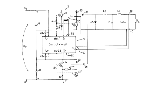
The circuit arrangement shown in Figure 1 includes two
equal converters generally designated 2 and 4, respectively.
The converters 2 and 4 have series connected inputs including
each an input capacitor 6 and 8, respectively. More
particularly, the capacitors 6 and 8 are connected in series
with each other between input terminals 10 or 12,
respectively, of the circuit arrangement. Each of these
converters 2 and 4 contain a current-mode controlled converter
bridge, of which one diagonal extends in parallel with the
corresponding respective input capacitor 6,8. The respective
other diagonal of said bridges contains a primary winding of
an output transformer 14 or 16, respectively.
In each bridge furthermore a transistor i8 or 22,
respectively, the primary winding of the transformer 14 or 16,
respectively, and a transistor 20 and 24, respectively, are
series connected in parallel with the respective input
capacitor 6 or 8. More particularly the first mentioned
transistor 18 or 20, respectively, is connected to the
positive side of the input capacitor 14 or 16, respectively,
and the direction of conduction of both transistors is from
the positive side. In each bridge furthermore a diode 26 or
30, respectively, the primary winding 14 or 16, respectively,
and a diode 28 or 32, respectively, are series in parallel
with the input capacitor 14 or 16, respectively. More
particularly the first-mentioned diode 26 or 30, respectively,
is connected to the positive side of the input capacitor 14 or
2~~~~~~
16, respectively, and the blocking direction of both diodes is
towards the positive side.
The secondary windings of the respective transformers
14,16 are connected in parallel to each other via rectifier
5 diodes 34 or 36, respectively, and operate in common on a load
RL connectable to output terminals 38 and 40. In the output
circuit leading to the output terminals 38, 40 a shunted
freewheel diode 42 is included followed by an output filter
Lli CliL2iC2.
The circuit arrangement illustrated in Figure 1 can be of
a kind known per se as regards the details thereof thus far
described above.
According to one aspect of the present invention the
circuit arrangement includes a control circuit effecting that
the current output from the converters 2,4 is regulated by the
output current pulses of the respective converter being
shifted with respect to each other essentially without change
of their width so that the mean value of the voltage over the
load is kept constant. In the control circuit, generally
designated 44 in Figure 1, this control is carried through,
indicated by means of dashed lines 46 in Figure 1, in a way to
be disclosed more in detail below by means of switching-on and
switching-off pulses to the transistors 18-24.
The regulation aimed at can be attained by shifting the
starting and stop times for the current pulses somewhat ahead
for the transistors of the converter having a low input
voltage. By the shifting ahead of the starting time the
current in the output filter has time to decrease somewhat
further before the filter starts drawing current from the
3o converter having a low input voltage.
As parameters for the control, indicated with ctrli and
ctrl2, the respective input voltages O1 and U2 of the
converters 2 and 4, as indicated at 48 and 49, respectively,
the output voltage U3 of the circuit arrangement applied over
the load, as indicated at 50, and the respective currents I1,
IZ, through the primary windings of the respective
transformers 14 and 16, as indicated at' S2 and 54,
respectively, are used.
Reference is now made to the principle diagram of the
6 ~~~3'~3'~
control circuit 34 in Figure 2 in connection with the curves
shown in Figure 3.
The two voltages U1, U2 are processed in a balance sensing
circuit 56 such that on one of the two outputs of the circuit
a first signal is obtained representing the difference between
the voltages, and on the other output a second signal is
obtained, being the inverted value of the first signal. The
first and second signals are fed to each one of two pulse
broadening circuits 58, 60. To a respective inverting input
l0 58', 60' of each pulse broadening circuit a clock signal from
a clock generator 62 is also provided, that consists of very
short negative pulses, which are thus inverted to positive
pulses. The pulse width can be approximately 3oons and the
cycle to acs.
The pulse broadening circuits 58, 60 operate such that at
the output of one of them a first trigging pulse appears
having the same width as the clock pulse, and on the output of
the other one a second trigging pulse is obtained which is
broadened in proportion to the difference between the voltages
O1,U2. These trigging pulses are designated E1 and E2 in
Figures 2 and 3. The current pulses of the two converters 2
and 4 are trigged on by the negative flanks of the respective
trigging pulses. This is performed via pulse shaping and
driving circuits 64 and 66, on the outputs of which the
signals ctrli and ctrl2 appear.
Which one of the converters 2 and 4 to be trigged on is
decided by a flank trigged bistable circuit 67, which in turn
is trigged by the clock pulse from the clock generator 62 on
the negative flank thereof. The point of time for the negative
flank indicates the maximum pulse width for the preceding
current pulse. The two outputs of the bistable circuit 67 are
connected to blocking inputs 64' and 66', respectively, of the
circuits 64 and 66. Activation of these blocking inputs brings
about that the corresponding output of the respective circuit
64, 66 for the signal ctrli and ctrl2, respectively is locked
in a position that prevents the transistors of the
corresponding converters 2, 4 to conduct. From this also
follows that every second of the pulses E1, E2 is superfluous.
As is furthermore illustrated at 68 and 70 in Figure 2,
2~~~,~~,~
7
voltages U(Ii) and U(I2) derived from the transistor currents
Ii and I2 (indicated in Figure 1 by the resistance in series
with the respective primary winding of the transformers 14 and
13), are added to a voltage level Q obtained by integration of
the difference between the voltage U3 and a nominal voltage
Dnom~ The resulting voltage is designated A in Figures 2 and 3
and can also be written as A=U(Ii)+O(I2)+Q.
A compensating ramp voltage of the kind indicated by way
of introduction is subtracted from the voltage A at 72, said
1o compensating ramp voltage being obtained from a ramp generator
74, the output voltage of which being designated B in Figures
2 and 3. According to one aspect of the present invention the
generator 74 is controlled by the signals on the outputs of
the balance sensing circuit 56, as indicated by the arrows
leading therefrom, so that the appearance of the ramp signal B
can be effected by an occuring difference, if any, between the
voltages Ui and U2. The ramp generator is also connected to
the outputs of the bistable circuit 67, as is likewise
indicated in Figure 2, for controlling the operation of the
ramp generator in a way which will appear more closely in
connection with the description of the embodiment shown in
Figure 6.
The voltage resulting from the subtraction at 72 is
designated C in Figures 2 and 3. The voltage C is fed to a
level detecting circuit 76 which switches over when the pulses
of the voltage C reach a stipulated switching-over level. The
voltage on the output of the circuit 76 is designated D in
Figures 2 and 3. The voltage C increases so that the circuit
76 switches over to high (D), which provides a stop signal to
the conducting transistor pair. This makes the current through
the transistor pair to disappear, O(I1) (or U(I2)) then
decreasing to zero (A). Thereby also C decreases enough to
make the circuit 76 to switch over and D to go low again. Thus
the stop inputs of circuits 64 and 66 are not really flank
trigged.
In Figure 3 full lines indicate the currents I1 and I2 and
curve shapes A-Ei,E2 when there is balance between the
converters 2 and 4, i.e. when U1=02.
Depending upon the difference between the voltages U1 and
8
U2 at unbalance, and depending upon the output signals from
the balance sensing circuit 56, a modification of the output
signal of the ramp generator 74 occurs on the one hand, and a
broadening of one of the trigging signals from the circuits 58
and 60 on the other hand. Dashed lines illustrate in Figure 3
the change the curve shapes are exposed to if U1 is somewhat
greater than U2.
When the input voltage to one of the converter halves
increases/decreases, the slope of the current ramp (I1 or I2)
1o will increase/decrease to a corresponding degree, since the
slope is proportional to the difference between the input
voltage and the output voltage transformed to the primary side
(the output voltage is constant). The changes of the slope of
these signals are compensated by the change of the
compensating ramp, cf. the dashed lines of I1 and I2 and the
curve H, respectively, so that the slopes of the curve C
remain unchanged or are overcompensated.
The upper profile of the curve A corresponds to the
current in the output inductor L1. The negative ramps marked
in the diagram (curve A) thus do not actually belong to the
curve A. The current of the output inductor is of central
importance, since the invention is based upon the intention
that this current shall have time to decrease more before it
is taken from the converter with low input voltage, than when
it is taken from the other converter. As regards the curve A
for the rest, it can be noted that the signal Q in the time
perspective of interest is a signal of constant level.
The modification of the ramp voltage leads, via the
function of the level detecting circuit 76, to the changed
position shown with dashed lines of the stop pulses to the
circuits 64 and 66. Due to the fact that, as mentioned, the
starting and stop times for ctrli and ctrl2 are determined by
the negative flank of the trigg impulses E1 and E2, and of the
position~of the spikes D, respectively, this results in the
case of interest in the postponment of ctrl2 illustrated in
Figure 3. This in turn implies attainment of the desired
result that the current pulses through the converters shall be
shifted with respect to each other.
As should have appeared from the above the invention
20537 3 7
9
builds upon the principle that the relation between the
current output in the converters is regulated by the current
pulses being shifted in relation to each other without
changing their width during continuous operation. From the
geometry of the shape of the pulses C a condition for keeping
the width of the pulses constant can be derived, viz. that the
positive slope of the pulses should be the same from pulse to
pulse. This condition is fulfilled also in case of different
part input voltages to the converters by the aid of trailing
edge adjustment. The positive slope of the current Ila or I2,
respectively, is a function of the input voltage and if the
part voltages are different the positive slope of the
respective current pulses will be different, resulting in the
widths of the pulses becoming somewhat different. The error
appearing is normally very small since the balancing circuit
normally maintains balance. Practical experiments have,
however, shown that leading edge adjustment cannot alone
maintain balance at high output currents, i.e. when the
current pulses are high. Trailing edge adjustment solves the
problem with changes in pulse width by broadening one of the
pulses somewhat, at the same time as the other pulse is made
somewhat thinner so that normal pulse width is restored.
An embodiment of a more detailed circuit solution of the
cooperation between elements 56-62 in Figure 2 is shown in
Figure 4, and is illustrated more closely by means of the
diagrams in Figure 5. In the last-mentioned Figures only as an
example the values of certain components and voltage levels,
respectively, are given.
The two voltages U1 and UZ to be balanced are received in
the block 56 and are measured with each an insulating
amplifier not shown. The measured signals designated Ucibal
and Uc2bal, are fed into a differential amplifier 78. The
obtained signal, designated F is fed into an inverter 80 on
the one hand and into the first pulse widening circuit 58 on
the other hand. The inverted signal, designated G, is fed into w
the second pulse widening circuit 60.
The clock generator (not shown in Figure 4) emits the
clock signal H which according to the above consists of very
short pulses with a pulse width of approximately 300 ns and a
:.
to ~~~J~~~~
cycle of 10 ~,s. The clock signal sets to zero a ramp generator
consisting of a capacitor 86 via two parallel amplifiers 88,
90 and a transistor 92. The base signal to the transistor 92
is designated I and the ramp signal over the capacitor 86 is
designated J.
Each of the pulse widening circuits 58, 60 includes a
comparator 94 or 96, respectively. The ramp signal over the
capacitor 86 is fed to the respective positive inputs of the
comparators 94 and 96. The voltage on said positive input will
deviate somewhat from the voltage J due to the series
resistance designated 98 which, however, may be neglected.
Signals resulting from the signals F and G on the respective
negative inputs of the comparators 94 and 96 are designated R
and L, respectively.
The output voltages from the comparators 94 and 96,
designated M and N, respectively, are fed to one of the inputs
of each a NAND-gate 100 and 102, respectively. To the second
input of the NAND-gates a clock signal H is fed, and the
outputs of said gates form the outputs of the respective pulse
widening circuits 58 and 60. The corresponding output signals
are designated o and P, respectively, corresponding to the
signals E2 and E1.
A feed back loop extends from the output of each NAND-
circuit to the negative input of the respective comparators
via circuits 104 and 106, respectively, each consisting of a
resistance and a capacitor in parallel. The small cuts of the
curves R and L, being amplified in Figure 5 for the sake of
clearness, originate from this positive feedback and result in
secure and distinct switching over of the comparators.
When the clock pulse time 300 ns has passed, the
comparators 94 and 96 can provide a negative flank on the
respective output when right time has been attained. The times
are determined by the time passing before the ramp signal J
reaches the same level as the respective input voltages R and
L, affected by the said positive feedback and appearing on the
negative inputs of the comparators. In the example shown the
clock signal H directly affects the NAND-gate 100 which
switches over essentially immediately, this in turn affecting
the input voltage R via the feedback so that the comparator 94
11
switches over and gives rise to the output voltage M. The
comparator 96 does never switch over, due to the fact that the
voltage L all the time lies below the ramp signal J, this
consequently resulting in the output voltage N shown.
The positive flanks of the output voltage O from the NAND-
gate 100 are determined only by the negative flank of the
clock pulse H and the delay of the NAND-gate. The time of its
negative flank is determined by the time of the positive flank
of the clock pulse H added by the time determined by the ramp
signal J, and the delay of the comparator and the NAND-gate.
The curve shape of the output voltage P from the NAND-gate
102 is a direct inversion of the clock pulse H with associated
gate delay.
An embodiment of a more detailed circuit solution for the
generation of the ramp signal B is shown in Figure 6.
The ramp generator 74 comprises as a main component a
capacitor 110 and a zero setting transistor 112. The ramp
signal over the capacitor 110 is a voltage signal which by
means of a transistor 114 and resistor 116 is converted to a
2o current signal.
The slope of the compensating ramp is decreased in
proportion to the magnitude of the deviation from balance,
i.e. between the voltages U1 and 02. This is obtained by means
of the voltages F and G obtained as described above from the
balance sensing circuit 56 via diodes 118 and 120,
respectively, connected for receiving these voltages.
Resistors 122 and 124, respectively, and transistors 126 and
128, respectively, give a contribution to the slope of the
ramp which is twice as great as the decrease via the diodes
118 and 120, respectively. The bistable circuit 67 connected
to the ramp generator as described above chooses via resistors
130 and 132, respectively, the ramp pulses which are to
receive contribution, and the ones which are not.
To sum up, the slope of all ramp pulses fs first
decreased, whereupon twice as much as that removed is added to
every second pulse, cf. the dashed ramps of the curve shape B
in Figure 3.
Figure 7 only very shematically indicates a possible
embodiment of the pulse shaping and operating circuits 64 and
,.
12
66 indicated earlier in the form of blocks in Figure 2. The
dimensioning values included in the diagram shall, of course,
only be regarded as examples. The circuit 64, 66 comprises on
its two inputs two monostable circuits 140, 142. The trigging
signals E1 and E2, respectively, are fed to the flip-flop 140
which switches over on the negative flank of the signals. On
the output of the circuit the two signals ctrll and ctrl2 are
obtained in the way indicated in the Figure. The closer
accomplishment and function of the circuit 64, 66 should be
clear to the man of the art without any further explanations
here.
Of course, the invention is not limited to the embodiments
described above and shown on the drawings but can be modified
within the scope of the following claims. Thus, it should
particularly be noted that the invention is not only usable in
a circuit arrangement of the kind shown in Figure 1, which is
a current mode so called "double forward" circuit with series
connected inputs, but also as well in e.g. a current mode half
bridge of a kind indicated in Figure 8. The problem of such a
current mode half bridge is described on page C3-4 in a
publication from the company Unitrode 1986 with the title
"switching Regulated supply Design seminar Manual".
Furthermore the invention can be used in certain types of
converters intended for this continuous operation, wherein
possibly only the leading edge adjustment need to be used. The
leading edge adjustment functions alone excellently at low and
middle high output currents, more porely at high ones. It
works in two different modes: Besides the position of the
current pulses only their amplitude is affected at middle high
output currents, whereas at discontinuous currents amplitude
and width are affected besides the position.
The trailing edge adjustment functions alone excellently
at high and middle high loads, and not at all at low ones. At
low output curient, when the output choke approaches
discontinuous operation, there is a risk for locking due to
the regulation characteristic changing sign. The trailing edge
adjustment only changes the width of the current pulses
whereas the leading edge adjustment, during continuous
operation of the output choke, essentially varies the position
13
and amplitude of the current pulses.