Note: Descriptions are shown in the official language in which they were submitted.
WO 91/14281 PCI'/EP91/00426
` 20538~9
. 1
.
ETCHING METHOD FOR OBTAINING AT LEAST ONE CAVITY
IN A SUBSTRATE AND SUBSTRATE OBTAINED BY SUCH METHOD
_ . .
This invention concerns an etching method for obtaining at least
one cavity in a substrate and a substrate obtained by this method,
such method in particular being adapted for micromachining of small
p1ates in the micromechanical domain. The element to be etched is
often a plate of semiconducting material such as a silicon wafer.
It is sometimes necessary to provide cavities in such a wafer
having a substantially flat bottom with different depths. Although
it is obviously possible to obtain such cavities sequentially, it
may be readily seen that such a solution is not advantageous since
it requires as many masking operations and as many etching opera~
tions as there are cavities to be obtained .
Patent document JP-A-58/98927 describes an etching method
enabling the simultaneous obtaining of cavities having different
depths. This method comprises an anisotropic etching step followed
by an isotropic etching step. During the first step, the cavities
are formed with inclined sides, the etching stopping as soon as the
sides come together. It is thus understood that the maximum depth of
such a cavity is a function of the surface dimension of the latter.
The second step (isotropic etching) has as effect to increase the
depth of all the cavities to the same amount.
This method shows-a certain number of disadvantages. First of
all, it is not possible to form two cavities of the same surface
area and of different depths, nor a deep cavity of small surface at
.
the same time -as a- shallow cavity of large surface, since the
etching speed is the same for all cavities and the maximum depth
during the first step is directly proportional to the surface of the
cavity. ~ F
Furthermore, this method does not enable obtaining a flat
surface in all cavities, certain among them having to the contrary a
V-shape bottom.
W O 91/1428t PCT/EP9l/00426
~ 2
Next, this metod does not enable one to control exactly the
depth of all the cavities. Effectively, as has been shown in figure
1 of the above mentioned document, if one wishes to form two cavi-
ties having different surface areas exhibiting between themselves a
difference in depth less than the difference between their respec-
tive maximum depths, it is necessary to stop the etching of the
cavity having the greatest surface before its maximum depth is
attained. Thus, the moment when it is necessary to stop the etching
may not be determined in a particularly precise manner since the
etching speed can only be roughly estimated.
This invention has as its purpose to overcome the disadvantage
of known etching methods. Such purpose is attained by the claimed
method.
This method essentially consists in a first step of effecting an
anisotropic etching through a mask partially covering the zones to
be etched in order to form in each zone a set of V grooves, the
depth of which depends on the width of such section. The depth of
the etching in each zone is in this manner perfectly defined. In a
preferred manner, the etching patterns assume the general form of
rectangles. The latter are advantageously parallel to one another.
The second etching step, likewise anisotropic, increases uni-
formly the depth of each cavity. The difference in depth between two
cavities thus remains perfectly defined. Such second etching step
enables the obtaining in each cavity of a bottom which is substan-
tially flat.
This may be profitably employed so as to control in a zone the
thickness of a membrane or the depth of a cavity. It suffices in
effect to etch during the first step such zone and another zone,
referred to as the control zone, over depths such that during the
second step the desired thickness for the membrane or the desired
depth for the cavity are attained when the depth of the cavity ~n
-the control zone attains a precise and optically determinable value.
This control depht may for instance be the thickness of the wafer or
substrate. ~ `
The characteristics and advantages of the invention will be
better brought forth in the description to follow given by way of
- non-limiting illustration and referring to the attached drawings.
W O 91/14281 PCT/EP91/00426
1 3 20~3859
- Figures la to le illustrate the obtaining of two cavities of
different depths with the method according to the invention;
- Figure 2 shows an application of the method according to the
invention;
- - Figures 3a to 3d show how the depth of a cavity or the
thickness of a membrane may be controlled by the method according to
the invention;
- Figures 4a and 4b show respectively, seen from above and in
cross-section, different forms of bands or rectangles capable of
being employed in the first step of the method of the invention, and
the grooves in V form resulting in the case of a misalignment of the
bands relative to the crystallographic orientation of the wafer-or
substrate to be etched, and
- Figure 4c is an enlarged view of a portion of a figure 4a.
The invention is applied in particular to micromechanics for the
etching of semiconductive substrates. The method of the invention
essentially comprises two etching steps which are to be described
having reference to figures la to le.
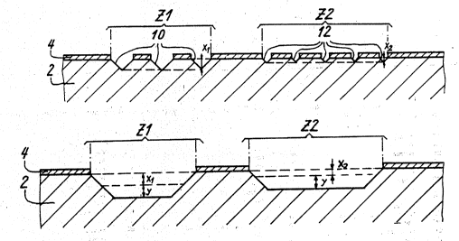
A substrate 2 of monocrystalline Si of orientation ~100> is
covered by a mask formed from a layer 4 of SiO2 (or Si3N4) of
thickness 1 ~m. In the zones Zl and Z2 to be etched, this layer has
been eliminated in order to leave open in each zone the etching
patterns forming parallel bands 6 (zone Zl) and 8 (zone Z2), visible
in cross-section on figure la. These bands may have a length equal
to the dimension of the cavity to be formed in the direction perpen-
dicular to the cross-section of the figure. They may also be clearly
- shorter (see figure 4a). The zones may have for instance a width of
about 0.1 mm to 5 mm, the bands 6, 8 of about 5 to 50 ~m and the
bands (spacers) of SiO2 of about 10 to 20 ~m. The number of bands 6,
8 per zones is generally in the order of 5 to 100."
The forming of the mask being well known in the technical field
of the invention, there is no necessity to describe this in detail.
It is-simply sufficient to recall that after having formed a full
layer of SiO2 and a full layer of photosensitive resin, this latter
is selectively insolated in order that the portions of`the-resin
situated above bands 6 and 8 to be formed may be eliminated by
dissolving in a developer solution such as xylene. Thereafter, one
, ~
. . .. . . -
... ..
W O 91/14281 PCT/E Wl/00426
~3o~9 q '-
eliminates the unprotected part of the SiO2 layer by chemical
etching with a solution of HF/NH4F (the substrate 2 of Si is not
attacked by this chemical agent) and one next eliminates the resin
mask (figure la), for instance with a solution of HN03.
S One then proceeds to the anisotropic etching of substrate 2 by
chemical attack with a solution of KOH. Aqueous solutions of KOH
with and without 2-propanol have been employed with success. Other
solutions may be used; one may in particular refer to the article
"Silicon as a Mechanical Material" by K.E. Petersen, which appeared
in Proceedings of the IEEE, vol. 70, Nr. 5, May 1982, pages 420-457
(in particular: table II, page 424).
One thus obtains recesses in the form of Y grooves 10 (respec-
tively 12) the width xl (respectively x2) of which in zone Z1
(respectively Z2) depends on the width of the bands in such zones
(figures lb). As the etching stops by itself when the sides of the
grooves come together, the maximum depth of the etching is strictly
defined by the width of the band (to the extent that the mask is not
affected in a significant manner by the etching solution). There is
no risk of overetching and, consequently, one may without disadvan-
tage leave the etching to be continued sufficiently long in order to
be certain that the maximum depth is attained.
The second etching step is applied to zones Zl and Z2 in their
entirety. It is thus necessary initially to eliminate the layer 4 of
SiO2 covering these zones. For this, a mask of photosensitive resin
is provided in a layer 14 (figure Ic) and the poPtions 16, 18 of the
layer SiO2 covering the zones Zl and Z2 are eliminated by chemical
attack in a solution of HF/NH4F. Then, the resin mask is itself
eliminated (figure ld). It should be emphasized that the mask of
resin does not need to be exactly positioned relative to zones Zl
and Z2. It suffices that -it leaves open parts 16 and 18 of these
zones.
One can then proceed to the second step of anisotropic etching
of the substrate in a solution of KOH. The depth y of the etching
during this step is the same in both cavities and depends directly
on the etching time (figure le).
On figure le the bottom of each cavity is perfectly flat. This
however is a schematic representation. In reality, the etching speed
. ~ ~-. .. .... ~ .- - . .
W o 91/14281 PCT/EP91/00426
20~38~9
being greater laterally than vertically, the grooves are enlarged
little by little up to the point of coming together. In other words,
the bands situated between two grooves see, little by little, their
width and their height diminishing. Thereafter, the free sufaces of
zones Z2 and Z2 visible on figure ld become more and more planar as
the etching depth y increases. However, in general, it remains
possible, sometimes even with the naked eye, to distinguish undula-
tions in the bottom of the cavities recalling the pattern of the
initial mask of SiO2. By way of example, it has been possible to
observe undulations of around 1 ~m amplitude.
The method according to the invention enables a better control
of the form of the cavity than known methods. Effectively, it is
known that the lateral overetching of a surface depends on the size
and the form of such surface. Lateral overetching is thus important
lS with known methods in which the totality of a zone is exposed to the
etching during the entire procedure. On the contrary, in the method
according to the invention, the first etching step is applied to
etching patterns much smal1er than a zone. Thus, whatever the form
of the zone to be etched, lateral overetching is limited during the
first step of the etching. This may be advantageously employed in
order to form a cavity or a hole for which one wishes to have a good
control of the dimension.
The method described having reference to figures la to le
enables one to obtain simultaneously at least two cavities having
2~ different depths and for which the difference between such depths,
egual to xl-x2, is defined with great precision. Let us note that
approximatively the same result could be obtained in etching zone Z2
only during the second step of the etching. It is sufficient for
this to form grooves in Zl having a depth of xl-x2, during the first
etching step and to etch the two zones Zl and Z2k over a depth of
x2+y, during the second etching step.
It should be further noted that the different etchéd zones may
be distant from one another, as shown on figures la to le, or
contiguous.-In the latter case, one obtains a single cavity exhibi-
3~ ting portions having different depths. -
Figure 2 illustrates an application of the method of the inven-
tion. A substrate 20 of monocrystalline Si of orientation ~100> and
,
w 0 91t14281 PCT/EP91/00426
~3~9 6 ~ ~
of a thickness of 200 ~m is machined by chemical attack in order to
form a membrane 22 of 8 mm diameter and of 100 ~m thickness. A
piezoelectric disc 24 provided on each side with a conductive
element each of which forms an electrical conductor 26, 27 is glued
onto one of the sides of the membrane. One may thus cause a strain
in the membrane (movement along the axis perpendicular to the plane
of the membrane). This type of membrane is in particular employed in
micropumps intended in the medical domain for the injection of
medicaments in solution, the principle of which is described in the
article "A piezoelectric Micropump Based On Micromachining of
Silicon" by H. van Lintel et al. which appeared in Sensors and
Actuators, vol. 15, 1988, pages 153-167.
As may be seen on figure 2, local overetching is brought about
in zone Z3 of the membrane in order to take into account the extra
thickness formed by electrical conductor 26. It would be possible to
avoid such overetching by gluing an electrical conductor 26 covering
completely the piezoelectric disc, but there would then be, between
the piezoelectric disc and the membrane, a first layer of glue, the
electrical conductor, and a second layer of glue, which would bring
about a dispersion of the motion characteristics between different
membranes during utilization of the latter.
The etching of the upper surface 28 (that on which the piezo-
electric disc will be glued) of substrate 20 i5 effected in two
steps in accordance with the invention. It should be noted that the
lower surface is also etched in this particular case.
In the first step, only zone Z3 is subjected to etching; this
etching is effected through a mask leaving open a set of parallel
bands in order to produce a set of Y-grooves. In the second step,
the etching is effected through a mask leaving open the totality of
the surface of membrane 22 to be obtained. The depth of the V-groo-
ves defines the depth of the cavity of zone Z3 relative to the
membrane. ; - -
The method of the i m ention may also be employed ~in order tocontrol the depth of etching and to assure thus that the cavities
have exactly the desired depth and/or that the membranes have
exactly the desired~thicknesses.
w o 91/14281 PCT/EP91/00426
7 20538~9
Let us suppose one wishes to form a cavity of depth y4 in a zone
Z4 of a substrate having a thickness e. For this one will create a
control cavity in a zone Zc according to the method of the inven-
tion.
5One thus forms in the control zone Zc a mask leaving uncovered a
set of parallel bands 30 (figure 3a). Such mask is formed for
instance in a layer 32 of SiO2 in the case of a substrate 34 of
monocrystalline Si. The width of these bands is chosen in order that
through anisotropic etching the depth of the V-grooves 36 formed in
zone Zc is equal to e~y4 (figure 3b).
One then e1iminates the protective layer 32 above zones Z4 and
Zc (figure 3c) and one proceeds with the anisotropic etching of the
latter. The depth y4 is attained in zone Z4 approximatively at the
same instant as a hole is formed in the control zone Zc (figure 3d).
This instant is thus easily detectable by visually observing the
control zone Zc.
The same method may be employed in order to obtain a membrane of
a given thickness E. It is sufficient in effect to form grooves in
the control zone of sufficient depth, substantially equal to E (the
precise value depends on several parameters including the nature of
the etching substance) during the first etching step. Thus, during
the second etching step, a hole is formed in the control zone Zc
when the thickness of the membrane is equal to the desired value E.
It should be noted that it is not necessary to know the thickness e
of the substrate in order to obtain the desired membrane according
to this method.
- Instead of detecting the formation of a hole, one could also
detect, for instance just before the hole is formed, a change in
colour of the membrane in the control zone Zc andtor-a variation of
the transparency of the membrane in this zone.
A method is known in which a single groove is etched in the
control zone 2c, the dimension of this zone being chosen in order
that the depth of the groove corresponds to the thicknéss of the
membrane. The optical detection of the end of the principal etching
according to the known method, which is effected from the side of
the substrate opposite to that in which the control groove is
- : .
- , ,
., '. ~ . . .: :
.
- . .. ... ~ ~ .. .. . .
WO 91/14281 PCI/EP91/00426
~ 3~9 8 "_ ~
etched, is much more difficult since, instead of forming a hole, as
in the method of the invention, one must detect a simple slot.
In the method described having reference to figures 3a to 3d,
zone Z4 is etched only during the second etching step. One may
however also etch this zone during the first etching step in order
to form V-grooves therein. It is sufficient simply to choose the
width of the bands to be etched in zone Z4 and Zc in such a manner
that the difference between the depth of the grooves in the control
zone Zc and the depth of the grooves in ~one Z4 are equal to the
residual thickness which one wishes to obtain in zone Z4 after the
second etching step. ~n figure 3b, where only the control zone is
etched during the first etching step, the depth of the groove is
thus equal (in practice about equal) to the residual thickness of
zone Z4 on figure 3d).
One also finds in the article "An IC Piezoresistive Pressure
Sensor For Biomedical Instruments" by Samaun et al. published in
IEEE Transactions on Biomedical Engineering, vol. BME-20, Nr. 2,
March 1973, pages 101-107 (particularly figure 6) a method in which
a wafer is etched on one side in order to form a membrane and the
other side of which is simultaneously etched in order to form a
frame surrounding the membrane, each side of the frame being a
V-groove, the depth of which is equal to the desired thickness of
the membrane. When the thickness of the membrane attains the depth
of the Y-grooves, the portion of the wafer inside the frame falls
away, leaving a hole of large dimensions readily visible.
With this known method, there is no indication enabling one to
observe that one is close to the instant when the etching must be
stopped.
Furthermore? in order that the hole appear and be visible at the
end of the etching, it is necessary that each side of the frame be
formed with a single groove having a substantial length (the latter
is in the order of a millimeter).
It has;been assumed up to the-present that the width of the
V-grooves was equal to the width of the bands left uncoYered by the
protection mask, i.e. the width of the sides of the frame. This is
exact when the direction of the bands is strictly oriented at 45
(line A-A on figure 4a) relative to the two crystallographic axes
"' ' . ~ , ' ' .
. .
.
, . .
WO 91/~4281 PCr/EP91/00426
20~3859
which define the plane of a Si plate of ~100> orientation. On the
other hand, the grooves are wider than the bands and consequently
deeper than foreseen if the bands are not perfectly at 45 relative
to such axes. The method described in this article does not permit
in this case a good control of the thickness of the membrane to be
formed .
To the contrary, the method of the invention enables one to
avoid the consequences of a poor alignment. The effects of a poor
alignment appear clearly on figures 4a and 4b which show respecti-
vely, seen from above and in cross-section alsng line IV-IV a
substrate 38 covered by a mask 40 in which bands having different
forms and orientations have been provided.
Band 42 is perfectly parallel to line A-A. The V-groove 44
formed by anisotropic etching has thus exactly the width of this
band.
On the other hand, band 46 is not perfectly parallel to line
A-A. The V-groove 48 is then wider than band 44 because of etching
under layer 40 up to the edges 50, 52. There also results therefrom
a depth of groove greater than desired.
It is noted that the enlarging of the groove depends on the
length of the band. One may reduce this phenomenon of enlarging and
consequently deepening of the grooves by replacing the band 46 by a
series of disjointed bands 54. One then obtains V-grooves 56 the
enlarging of which, relative to groove 44, is less than with the
band 48.
One may further reduce this enlarging by diminishing the width
of the end portions 58 of band 60.-The-width of each groove 62 is
thus fixed by the width of the central portion 64 of the segments.
As may be seen on figure 4c which shows a band 60 in enlarged
form, the width of the groove is reduced on each side by a value d
relative to the groove obtained with a band 54.
The increase of the width of groove 62 relative to groove 44
thenj becomes almost negligible.:The same follows in respect to the
increase of the depth.
- , .: , - . . . . :
,
". : . - ~ . . .